2004 E E E Asia-Pacific Conference on Advanced System Integrated Circuits(AP-ASlC2004)/ Aug. 4-5,2004
14-6
A
Low
Power SGb/s Transimpedance Amplifier with Dual Feedback Technique
I-Hsin Wang, Chung-Shun
Liu,
and Shen-Iuan Liu
Department of Electrical Engineering &
Graduate Institute of Electronics Engineering
National Taiwan University, Taipei 1061
7,
Taiwan
Abstract-This paper presents the design and implementation of a SGb/s transimpedance amplifier (TIA) with dual shunt-shunt feedback technique to enhance the circuit performance. Measured bandwidth is 4.9GHz and measured transimpedance gain is 60 dB R. The chip consumes only 8mW at
0"tp"l
z w cl
M1 M2 U P i
1.8V supply voltage and occupies 650pmx500pm in lnpul
i T
a 0.18pm CMOS process. MS
i I. Introduction
The recent growth in the optical fiber e i a s miwOtk+ core amplib, +eYner+
communication industry has resulted in high demand for low-cost high-performance optical front ends. One of the critical components of the optical fiber receiver front end is the transimpedance amplifier. A TIA requires high transimpedance gain, high bandwidth, low input impedance, and low power consumption. However, the power consumption trade off with gain and bandwidth product. In this paper, the proposed dual shunt-shunt feedback network used to improve this trade off.
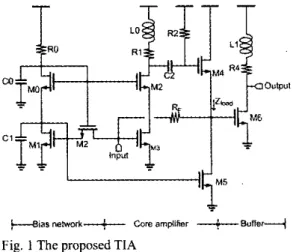
Fig. 1 The proposed TIA
One of the dual shunt-shunt feedback networks in the proposed core amplifier is composed of the MOS transistors M2
-
M4, AC couple capacitor C,, and feedback resistor R F . Assume the amplifier exhibits a mid hand gain Aoand one pole at 6 ~ 0 , thenits transfer function is given by Equation (1).
The transfer function of a TlA can be given as
Vo,,, A,&
- ( s ) = -
11. TIA architecture
The complete architecture of the proposed TlA is I," R , C , s ' + ( R , C , , + - ) s + I A, + 1 ( 2 )
. .I
depicted in Fig. I . It consists of a bias network, core 0 0 0 0
amplifier, and the output buffer. A. Core amplifier
The core amplifier, depicted in Fig. 1, has to provide a sufficient voltage gain so as to increase the TIA's bandwidth and make its Z,, very close to RF. In
this amplifier, the cascode common source amplifier can eliminate the Miller capacitance effect. However, large capacitance due to photodiode's parasitic effect makes the design more difficult. In order to minimize the power dissipation, the inductive peaking technique [ i j is utilized in this circuit, since it does not occupy additional voltage headroom and can improve the speed effectively.
where it is assumed that A. >> I , and Cpo is the photo diode capacitance. Usually, it is a typical second order system. The denominator of a second-order transfer function is expressed as s*
+
2 5 ~ ~ s+
on2,
then
E ,
the "damping factor," must be equal to&I2
for critical damping. Rewriting (2), we haveWhen
5
= & / 2 , then(4)
Thus, the -3dB bandwidth of the core amplifier must
2004 E E E Asia-Pacific Conference on Advanced System Integrated Circuits(AP-ASIC2004)/ Aug. 4-5,2004
be chosen equal to twice the closed-loop bandwidth of the first-order TlA to ensure a critical-damped response. With the above condition for critical damping, the -3dB bandwidth of the TIA is
From equation (2) and
(9,
we have to choice RFcarefully to trade off between transimpedance gain and bandwidth, In ow TIA, we take the
RF
equals I k n for 60dB transimpedance gain in bandwidth better than 5GHz without photo diode capacitance loading.Between the first stage and the source follower, a capacitor ( 0 . 8 ~ ) for ac coupling is connected. This is because we need large bias current in the first stage to provide sufficient voltage gain but will results in a lower dc level. If we apply dc couple between the two stages, the output dc level of the source follower will be too low to tum on the buffer transistor. The bias resistor of the source follower is realized by a PMOS operating in the triode region.
For the cascaded circuits, they usually have a pole at each stage output due to loading circuit. In ow TIA circuit, there is a pole in the output of the core amplifier. If the loading impedance Zlo, is large, this pole will become dominated and decrease circuit bandwidth. In order to eliminate this effect on core amplifier's bandwidth, a second shunt-shunt feedback network is incorporated in the output of the core amplifier. This feedback network is composed of the MOS transistors M I -Mz and
Ms,
resistor RF, and capacitor C,. The transistor M2 is operated in triode region. Assume the capacitor CI is larger than the parasitic capacitance of the MOS transistors, C, andcxd. The on resistance of Mz is R,,2, and ro5 is the
output resistance of
Ms.
The loading impedance of the core amplifier can be written as2- = l + s C , ( R , + R m I )
[
c, +cna +- C ( R + R ) ) + 8 . , + ; i (6)s'c,c,,(R,
5,
It induces a zero and if one properly chooses the
value of C, and Ron>, the bandwidth can be extended
by canceling a pair of zero and pole. On the other hand, capacitor Cl short the AC signal to ground, the input signal will not go through transistor MS to the output. By this topology the bandwidth of the core amplifier can be enhanced without increasing power consumption.
B. Noise Optimization
To optimize the input-referred noise of a TIA, one must very carefully choose the size of the input device since it contributes most of the noise [Z].
Consider the simplified noise model shown in Fig. 2.
Fig. 2 Equivalent model for optimizing the input noise.
There are two main noise sources: the thermal noise current of the feedback resistor and the channel thermal noise current of input transistor. The expression for the input-referred current density is given by
(7) Where V,,,,, represents the output noise voltage due to the core amplifier and we have
Substituting equation (8) into (7), we can derive the complete form of input-referred noise
In (9), the second term can be neglected compared
2004 E E E Asia-Pacific Conference on Advanced System Integrated Circuits(AP-ASIC2004)I Aug. 4-5,2004
Chip Area ( .ff m') with the first term, where 0, , the unit gain
frequency of a transistor, equals to g d ( C,
+
CgJ.To optimize the spectral density of input-referred noise current, we should make g, = C,, .or or to choose the input transistor size such that C,
+
Cg,j =CpD. Although the above example tells us that when
C,
+
Cgd = CpD, the noise will be reduced to the minimum level. The transistor size will be quite large and makes it difficult to reach a high bandwidth. We have to choice the core amplifier architecture and circuit layout carefully for this trade off.C. Output buffer
In order to drive the 50R impedance of the oscilloscope, the output buffer should have a high current driving ability. In some recent researches, the common-source type amplifier has become a better choice. First, the output dc level is determined independent of the input dc level thus will not suffer from smaller voltage headroom. Second, the output matching can be achieved by simply place a 5 0 0
resistor or two IOOR resistor in parallel. Ill. Experiment results
This work has been fabricated in 0.18fim lP6M CMOS process and the die photo is given in Fig. 3. To measure the frequency domain performance, the TLA chip is probe-tested with network analyzer. The measured transimpedance gain, Z,, is given in Fig. 4. The measured -3dB bandwidth is 4.9GHz and the midband transimpedance gain is 60dBR. The measured eye diagrams are given in Fig.5. The eye diagrams at 2.5Gbps, 3.125Gbps and 5Gbps when the input equivalent current equals 30uA respectively. Not only the first eye diagram fits in with the OC-48 mask
very well
but also widely open at the data rate of 5GbIs.IV. Conclusion
In this work, a I.SV, 5Gbps low power transimpedance amplifier using dual shunt-shunt feedback technique is implemented on a standard 0.18um CMOS process. By this way, the circuit bandwidth can be enhanced and only has 8mW power
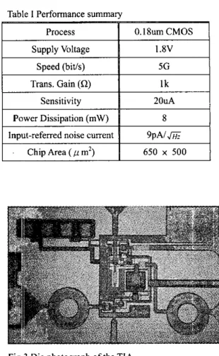
650 x 500 consumption. The characteristics of this circuit are listed in table 1.
Table 1 Performance summary
I
Process II
1.8V Supply VoltageI
Speed (bitls)I
5GI
I
Trans. GainK2)I
IkI
SensitivityI
20uA Power Dissipation (mW)I
8Fig.3 Die photograph of the TIA
Fig.4 The measured transimpedance gain
2004 IEEE Asia-Pacific Conference on Advanced System Integrated Circuits(AP-ASIC2004)/ Aug. 4-5,2004 - . 1 : . . . ... . . . . !$4Yh,w; ’ : - . . *., ~
***
(a) Eye diagram at 2.5GbisI ” ’ .. .. . . p ; , u I , ’ . . i . : . , . . . . , . : . . . . .
1 , .
. I . . . . : . . . . : . . . . ~ . . , . . . .i
. : . . . : . . : . . . : . . . . ! . (b) Eye diagram at 3.125Gbls I__---____ . . . . . . . . . . . . . .1
I i . . .j
. . . . . . , . . . ~ . . . . . . , ”“.;”).t . . . . ,,< F::,?v. (c) Eye diagram at 5Gbls Fig. 5 Measured eye diagramsREFERENCE
J. J. Morikuni and S. M. Kang, “An analysis of inductive peaking in photoreceiver design,” Journal of Lightwave Technology, vol. IO, pp. 1426 -1437, Oct. 1992.
A. A. Abidi, “On the choice of optimum FET
size in wide-band transimpedance amplifiers,” Journal of Lightwave Technology, vol. 6, pp. 64 -66, Jan. 1988.
S. Gala1 and B. Razavi, “1OGbis Limiting Amplifier and LaseriModulator Driver in 0.18um CMOS Technology,” Dig. Tech. Papers ISSCC, pp.188-189, Feb. 2003.
C. C. Tang, C. H. Wu, and S. 1. Liu, “Miniature 3D inductors in standard CMOS process,” IEEE Journal of Solid-state Circuits, vol. 37, pp. 471-480, April 2002.
J. M. Khoury, “On the design of constant settling time AGC circuits,” IEEE Transactions on Circuits and Systems 11: Analog and Digital Signal Processing, vol. 45, pp. 283 -294, Mar
1998.
M. Aiki, “Low-noise Optical Receiver for High-speed Optical Transmission,” IEEE Trans. Electron Dev., vol. ED-32, pp. 2693-2698, Dec.
1985.
H. H. Kim, S. Cbandrasekhar, C. A. Burrus, and 3. Bauman, “A Si BiCMOS transimpedance amplifier for 10-Gbis SONET receiver,” IEEE Journal of Solid-state Circuits, vol. 36, pp. 769 -776, May 2001.