電子工程學系 電子研究所
碩 士 論 文
適用於展頻時脈之多重交替式轉態取樣技
術與時脈資料回復電路
Clock and Data Recovery for Spread
Spectrum Clock using Multiple Alternating
Edge Sampling
指導教授:周世傑 博士
研 究 生:鄭元樸
時脈資料回復電路
Clock and Data Recovery for Spread Spectrum
Clock using Multiple Alternating Edge
Sampling
研 究 生:鄭元樸 Student:Yuan-Pu Cheng
指導教授:周世傑 博士 Advisor:Dr. Shyh-Jye Jou
國 立 交 通 大 學
電子工程學系 電子研究所碩士班
碩 士 論 文
A Thesis
Submitted to Department of Electronics Engineering & Institute of Electronics College of Electrical and Computer Engineering
National Chiao Tung University in partial Fulfillment of the Requirements
for the Degree of Master of Science in
Electronics Engineering December 2007
適用於展頻時脈之多重交替式轉態取樣技術與時脈資料回
復電路
研究生:鄭元樸 指導教授:周世傑 博士 國立交通大學 電子工程學系 電子研究所碩士班摘要
各式的高效能低成本串列傳輸技術廣泛應用於各種現代電子產品中,而時脈 資料回復電路則是高速串列傳輸系統的接收端中最關鍵的部分。現代時脈資料回 復電路設計的趨勢包括:隨著資料頻寬的提升與成本的下降,多通道的串列傳輸 已成為主流。而數位設計的時脈資料回復電路往往比類比電路設計更適合於此類 應用且不受製程/電壓/溫度變化的影響。另外,為了對抗電磁波干擾的問題,展 頻技術也被運用在資料傳輸內,因此時脈資料電路需要具備從展頻時脈中回復正 確資料的能力。 在本論文中,我們提出一個操作在 6Gbps,符合 SATA 第三代規格的時脈資 料回復電路。本設計具備了頻率合成迴路與時脈回復迴路之雙迴路,其各自獨立 的特性使得它適合應用在多通道的串列傳輸。而數位實現的時脈資料回復演算法 可針對不同應用而彈性調整其迴路特性,可增加應用性與可靠度。二階的數位迴 路演算法可以克服頻率上的誤差並可適用於展頻資料加以追蹤與回復,並符合 SATA 第三代的要求。在迴路中所使用之相位內插器高達 1/32 位元時間的相位解 析度使得相位追蹤誤差小而不致增加位元錯誤率。 在高速時脈資料回復電路中,二元相位偵測器是主流的趨勢。但是二元相位元相位偵測器的增益線性化,從而達到高速且穩定的相位追蹤。
實作晶片使用聯電標準臨界電壓 90 奈米互補式金氧半導體製程來製造,佈
局後之模擬的資料頻率為 5.5Gbps 到 6.5Gbps,回復時脈的峰對峰抖動值為
Clock and Data Recovery for Spread Spectrum Clock using
Multiple Alternating Edge Sampling
Student: Yuan-Pu Cheng Advisor: Porf. Shyh-Jye jou
Department of Electronics Engineering Institute of Electronics
National Chiao Tung University
Abstract
Recently, many high-speed and low cost serial link transmission technologies are
developed and are widely used in every modern electronic product. The clock and
data recovery module is the most important component in the receiver end of high
speed serial link systems. Modern trend of CDR circuit design includes: First, as the
increase of transmission bandwidth and the decrease of fabrication cost, multi-channel
transmission system has become the mainstream. Second, digitally implemented
CDRs are often more favorable than analog ones for the wide applicability and
robustness against PVT (process, voltage, temperature) variations. Finally, in order to
reduce EMI (electro-magnetic interference) problem, spread spectrum clock
technology is used in data transmission. Therefore it is necessary for CDR to recover
correct data from spread spectrum clock transmission.
In this thesis, we propose a CDR circuit that operates at 6Gbps and conform to
specifications of SATA generation three. This design incorporates dual-loop, the
digitally implemented phase tracking algorithm is programmable to change the loop
characteristic for different jitter conditions, enhancing the applicability. The 2nd-order
digital loop algorithm can track frequency deviation and is therefore suitable for
spread spectrum clock transmission. The tracking for SSC conforms to SATA
generation three specifications. In the loops, The phase interpolator has a resolution of
1/32 UI and is enough to keep phase error small and BER low.
In the high speed CDR, binary phase detection is the mainstream. However the
non-linear characteristic of binary phase detection introduces unwanted effects like
PD gain varies with jitter amplitude, and oscillatory steady state of phase tracking.
Therefore we propose the Multiple-Alternating Edge Sampling (M-AES) to linearize
the PD gain and acquire high speed and stable phase detection.
The test chip is fabricated in UMC 90nm CMOS regular-Vt process. The
post-layout simulated data rate from 5.5Gbps to 6.5Gbps, the peak-to-peak jitter is
17.52ps. The analog circuit power consumption is 55mW under 1.0V supply voltage.
誌 謝
首先我要感謝周世傑老師在我碩士生涯中細心的指導與鼓勵。從帶進混合信
號電路的領域到指導口頭報告的技巧,老師的指導讓我在求學生涯獲益良多。謝
謝老師對我們生活與做人處事的關心,老師口中「Study hard, Play hard」的
信念也讓我們的研究生活充實而愉快。祝福老師家庭幸福,也祝老師的研究群蒸 蒸日上。同時也感謝劉深淵教授、陳巍仁教授與蔡嘉明教授撥空參加口試,並賜 予寶貴的意見讓我的論文更加完整。 其次我要特別感謝林志憲博士在我研究過程中給予的引導,沒有他的幫助我 的論文變無法完成。謝謝他提供創新的想法與寶貴的經驗,同時每次的討論也都 讓我增長不少經驗。祝福喜事將近的您有美滿的婚後生活。 接著我要感謝在我的研究生活裡,曾與我共事的學長、同學、學弟與朋友們。 謝謝我研究的夥伴,彥穎。你對專業的認真執著與平時的風趣幽默形成很大的對 比,是我在研究與生活上的好搭擋。謝謝在製程與儀器上方面幫助我許多的志龍 學長與嘉琳學姐,謝謝昌敏學長、誌華學長和舌燦蓮花的瑋昌學長給了我愉快的 碩一實驗室生活。謝謝我的同學和朋友們:俊男、國光、俊誼、建君、宜興、珦 益、茂成、建甫、秉威,不論是大家一起打屁、電動、吃火鍋、羽毛球棒球,或 是出遊、爬山溯溪泛舟,你們的陪伴給了我精彩難忘的碩士回憶。謝謝實驗室的 學弟妹們,喻軒、舒蓉、昭安、祥牲、運祥,只能對你們說一句「下線尚未成功, 畢業仍須努力」,希望我們的成果對你們能有些幫助。另外要謝謝在新竹的教會 朋友們:詠麟、牧天、評任、宏瑋、梁軒、若琪、珮淇、沐恩,謝謝傅老師、慈 雲姐與潘傳哥,你們讓我的研究生活更有意義和努力的目標。願神祝福你們。
最後也最重要,我要感謝我的父母。謝謝你們給我無憂無慮的學生生活,體 諒我的忙碌,支持我的選擇。謝謝你們的付出和關懷,讓我可以朝我的目標邁進。 謝謝女友亭瑋的陪伴與支持,與你的相處讓我成長許多,成為更成熟負責的人。 我珍惜每次與你們的團聚,希望將來我能不負你們的期望。 鄭元樸 于 新竹交大 2007.12.31
Table of Contents
List of Figures ... iii
List of Tables ... v
Chapter 1 Introduction ... 1
1.1 Introduction of High-Speed Serial Link ... 1
1.2 Transceiver of the Physical Layer ... 2
1.3 Motivations and Goals ... 3
1.4 Thesis Organization ... 4
Chapter 2 Oversampling Based Clock Data Recovery ... 6
2.1 Introduction to Clock Data Recovery ... 6
2.2 Comparisons of Oversampling CDR Algorithms and Architectures ... 8
2.2.1 Blind Oversampling Scheme ... 9
2.2.2 Feed-Back Phase Adjusted Scheme ... 10
2.2.3 Feed-Forward Phase adjusted Scheme ... 12
2.3 Timing and Data Format Specifications ... 13
2.3.1 Data Format ... 13
2.3.2 Timing and Jitter Performance ... 14
2.3.3 Spread Spectrum Clock ... 16
Chapter 3 A 2nd-Order Phase/Frequency tracking Algorithm for Feed- Forward Phase Adjusted CDR ... 19 3.1 Overview ... 19 3.2 Phase/Frequency tracking CDR ... 21 3.2.1 Pre-Filter ... 22 3.2.2 Proportional Path ... 23 3.2.3 Integral Path ... 26
3.2.4 Phase Rotation Counter and Decoder ... 27
3.3 Phase Selection ... 30 3.3.1 Phase Multiplexer ... 32 3.3.2 Phase Interpolator ... 34 3.3.3 Data sampler ... 34 3.4 Simulation Results ... 35 3.4.1 Behavior Modeling ... 35 3.4.2 Circuits Simulation ... 42
Chapter 4 Multiple Alternating Edge Sampling (M-AES) Scheme ... 48
4.2 Edge sampling schemes ... 50
4.2.1 Proposed M-AES Scheme ... 50
4.2.2 Edge sampling schemes and PD output ... 52
4.2.3 Edge sampling schemes and Jitter performance ... 54
4.3 Implementation of M-AES Scheme ... 63
Chapter 5 Experimental Results... 67
5.1 Design flow and methodology ... 67
5.2 Layout ... 69
5.3 Measurement Considerations ... 71
Chapter 6 Conclusions and Future Works ... 73
6.1 Conclusions ... 73
6.2 Future Works ... 74
List of Figures
FIG.1.1TYPICAL ARCHITECTURE OF SERIAL LINK TRANSCEIVER. ... 3
FIG.2.1THE TRACKING TYPE CDR ... 8
FIG.2.2BLIND OVERSAMPLING CDR. ... 9
FIG.2.3THE BLIND OVERSAMPLING ALGORITHM USING CENTER PICKING SCHEME. ... 10
FIG.2.4FEED-BACK PHASE ADJUSTED CDR. ... 11
FIG.2.5FEED-FORWARD PHASE ADJUSTED CDR ... 12
FIG.2.6RECEIVER EYE DIAGRAM [31] ... 15
FIG.2.7THE TARGET JITTER TOLERANCE MASK.[32] ... 16
FIG.2.8MODULATION PROFILES AND THEIR CORRESPONDING SPECTRUMS (A)SINUSOIDAL (B)TRIANGLE (C)SAW-TOOTH ... 18
FIG.2.9TARGET SSC SPECIFICATION OF OUR CDR ... 18
FIG.3.1(A)THE CONCEPT OF 2ND-ORDER CDR.(B)THE PROPOSED 2ND-ORDER CDR. ... 20
FIG.3.2THE BLOCK DIAGRAM OF PROPOSED CDR. ... 22
FIG.3.3(A)THE IDEAL OPERATION OF DATA AND EDGE SAMPLING.(B)UNDER JITTERY CONDITION, THE OPERATION OF BINARY PD AND PRE-FILTER. ... 23
FIG.3.4(A)THE ARCHITECTURE OF PROPORTIONAL PATH.(B)THE OPERATION OF PROPORTIONAL PATH. (C)THE OPERATION WITH NEGATIVE VALUES. ... 25
FIG.3.5THE ARCHITECTURE OF INTEGRAL PATH. ... 26
FIG.3.6SIMULATED PHASE ERROR IN STEADY STATE (A) WITH (B) WITHOUT COUNTER TRUNCATION BIT. ... 28
FIG.3.7 A SIMPLIFIED PROPORTIONAL,INTEGRAL AND COUNTER GRAPH. ... 29
FIG.3.8THE MULTI-PHASE VCO AND PHASE SELECTION BLOCK. ... 30
FIG.3.9(A)THE PHASE MULTIPLEXER (B)THE PHASE INTERPOLATOR ... 33
FIG.3.10THE DATA SAMPLER (A)COMPARATOR (B)AMPLIFIER/LATCH ... 34
FIG.3.11THE DISCRETE-TIME MODEL OF THE PROPOSED CDR. ... 35
FIG.3.12THE DETAIL MATLAB MODEL OF CDR. ... 37
FIG.3.13SIMULATION RESULTS OF PERIODIC JITTER WITH CONDITIONS SHOWN IN TABLE 3.3 ... 38
FIG.3.14SIMULATION OF FIG.3.12(B) WITH GI=1/64 ... 39
FIG.3.15PHASE ADJUSTMENTS IN ONE SSC MODULATION PERIOD. ... 40
FIG.3.16PHASE TRACKING ERROR IN SSC&PJ SIMULATION ... 41
FIG.3.17SIMULATED JITTER TOLERANCE MASK. ... 42
FIG.3.19(A)K28.5INPUT PATTERN (B)VERIFICATION OF CDR FUNCTIONALITY. ... 44
FIG.3.20THE ROTATION OF 160 PHASE. ... 45
FIG.3.21THE COMPARISON OF GROUP GAPS AND PHASE STEPS. ... 45
FIG.3.22RECOVERED CLOCK JITTER IN NON-SSC SIMULATION. ... 46
FIG.3.23THE SPECTRUM OF RECOVERED CLOCK AND RX CLOCK IN SSC SIMULATION. ... 46
FIG.4.1THE PROPOSED MULTIPLE ALTERNATING EDGE SAMPLING ... 51
FIG.4.2PHASE STEP TRACK (A) W.O.AES(B) W.I.AES. ... 51
FIG.4.4DIFFERENT JITTER SIGMA CONDITIONS FOR COMPARISON OF PD OUTPUT. ... 53
FIG.4.4THE PD OUTPUTS FOR DIFFERENT EDGE SAMPLING SCHEMES. ... 53
FIG.4.5THE CALCULATION OF BER. ... 54
FIG.4.6THE ASYMMETRIC JITTER CONDITIONS. ... 55
FIG.4.7THE SIMULATION RESULTS OF ASYMMETRIC JITTER CASE 1. ... 56
FIG.4.8THE SIMULATION RESULTS OF ASYMMETRIC JITTER CASE 2. ... 57
FIG.4.9THE SIMULATION RESULTS OF ASYMMETRIC JITTER CASE 3. ... 58
FIG.4.10THE SIMULATION RESULTS OF ASYMMETRIC JITTER CASE 4. ... 59
FIG.4.11THE SIMULATED BER FOR Σ=0.02 ... 60
FIG.4.12THE SIMULATED BER FOR Σ=0.06 ... 60
FIG.4.13THE SIMULATED BER FOR Σ=0.10 ... 61
FIG.4.14(A)AESEDGE SAMPLING (B)DATA SAMPLING ... 65
FIG.4.15SIMULATION OF AES ... 66
FIG.5.1THE DESIGN AND IMPLEMENT FLOW OF CDR. ... 68
FIG.5.2LAYOUT VIEW OF TEST CHIP. ... 70
List of Tables
TABLE 1.1INDUSTRIAL STANDARDS OF HIGH-SPEED SERIAL LINK ... 2
TABLE 2.1GENERATIONS OF SATA[29] ... 13
TABLE 2.2THE PARAMETER OF RECEIVER EYE DIAGRAM ... 15
TABLE 2.3THE REQUIREMENTS OF JITTER TOLERANCE MASK. ... 16
TABLE 3.1THE OPERATION OF DIFFERENT COUNTER GAIN. ... 29
TABLE 3.2THE OPERATION OF PHASE SELECTION ... 32
TABLE 3.3SUMMARY OF FIG.3.13. ... 39
TABLE 3.4CDR SIMULATION SUMMARY ... 47
TABLE 4.1THE SIMULATED BER FOR Σ=0.02UI ... 62
TABLE 4.2THE SIMULATED BER FOR Σ=0.06UI ... 62
TABLE 4.3THE SIMULATED BER FOR Σ=0.10UI ... 62
TABLE 5.1THE PAD ASSIGNMENT OF TEST CHIP. ... 70
Chapter 1
Introduction
1.1 Introduction of High-Speed Serial Link
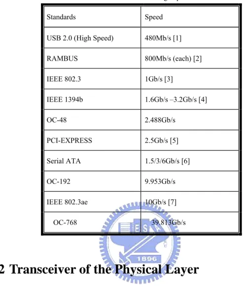
The prospering of multi-media application and communication has induced rapid growth of transmission bandwidth. The rapid growth of computing power and digital contents soon moves the performance bottleneck to the peripheral I/Os and network interconnects. As a result, a variety of high-speed and low cost serial link technologies are invented. The high-speed serial link plays major role in every modern electronic product, ranging from micro-structure within micro-processors, peripheral I/O, area networks, panel display interfaces, to inter-continental optical fiber networks. The common characteristics are low swing differential signals with current mode transmission because of the finite bandwidth of channel, low-power and noise immunity. A list of widely applied high-speed serial link standard is shown in Table 1.1[1]-[7].
Table 1.1 Industrial standards of high-speed serial link
Standards Speed
USB 2.0 (High Speed) 480Mb/s [1]
RAMBUS 800Mb/s (each) [2] IEEE 802.3 1Gb/s [3] IEEE 1394b 1.6Gb/s –3.2Gb/s [4] OC-48 2.488Gb/s PCI-EXPRESS 2.5Gb/s [5] Serial ATA 1.5/3/6Gb/s [6] OC-192 9.953Gb/s IEEE 802.3ae 10Gb/s [7] OC-768 39.813Gb/s
1.2 Transceiver of the Physical Layer
Fig. 1.1 shows the typical architecture of modern serial link transceivers. It includes a PLL as clock generator, Encoder, Decoder, PISO (Parallel In Serial Out), SIPO (Serial In Parallel Out), transmitter Driver, receiving Sample and Hold circuit, and an Equalizer. The Encoder and Decoder are composed of Scrambler and 8B/10B [8].
Scrambler provides advantages of data transition, encryption, and spread spectrum. 8B/10B coding is used for DC balance and provides enough transitions for clock data recovery to extract phase information, significantly increases the probability of detecting single or multiple errors during transmission. PISO converts the parallel data into binary sequence; conversely the SIPO recovers received data
Fig. 1.1 Typical architecture of serial link transceiver.
into parallel bus.
The transmitter Driver may use high speed current mode logic (CML) to drive data into impedance matched copper line, or use laser diodes to drive optic fiber. At the receiver, an Equalizer is often used in high transfer rate to conquer the attenuation from the band-limit effect of long distance channels. The Sample and Hold circuit samples the receiving sequence at the correct time point to extract correct data.
The clock and data recovery (CDR) circuit at receiving side is especially important due to high speed transfer rate and noisy environment. Its function is to synchronize the local clock to the receiving clock, eliminates phase and frequency errors and to put the sample point correctly at the data opening.
1.3 Motivations and Goals
The requirements of high data rate and highly integration of modern high speed serial link motivates the design of clock and data recovery circuit that is able to work at multi-Gb/s and is suitable in large scale integration.
adjusted CDR with Multiple Alternating Edge Sampling (M-AES) function. The CDR is able to track spread spectrum clock and is suitable for Multi-I/O integration.
The developing SATA generation 3 provides a good design example because of the high speed and similarity to a variety of modern high speed serial applications, such as HDMI [9] and PCI-E [5]. This work presents the design and implementation of a CDR applicable to SATA -III specifications. The specifications of SATA-III are investigated and become design target. The theory analysis and behavioral simulation will be carried out in MATLAB. The functional circuits designed in HSPICE and Verilog are simulated in mixed-signal simulator Nanosim. The test chip will be fabricated in UMC 1P9M 90nm 1.0V Regular-Vt CMOS process.
1.4 Thesis Organization
The thesis organization is described as follows:
Chapter 2 introduce the modern clock and data recovery circuits, including design trends from tracking type to various oversampling types of CDR. The specifications of data, timing and spread spectrum are also investigated.
Chapter 3 describes the 2nd-order Phase/Frequency tracking algorithm for Feed-Forward Phase Adjusted CDR. Algorithm and theories are analyzed; implementations, behavioral and circuit simulations are carried out.
Chapter 4 describes the Multiple Alternating Edge Sampling methodology used to improve CDR loop behavior. Theoretical analysis and implementation results are done and compared with different scenarios.
Chapter 5 shows the experimental results and describes the measurement consideration for the test chip.
Chapter 2
Oversampling Based Clock Data
Recovery
2.1 Introduction to Clock Data Recovery
In multi-gigabit serial link systems, due to the extremely high data rate, the bit time becomes small comparing to signal propagation time. It is therefore impractical to provide additional serial clock with a separate wire because even the slightest difference in length of the data and clock line will introduce significant skew. In modern high speed serial links, the clock is no longer transmitted through the channel, but is extracted from the data by the clock and data recovery (CDR) circuits. The CDR must detect the phase and frequency information from the received data transition and adjust the local clock generator to recover the link clock signal. The recovered clock is then used to sample the received data stream at the optimal point,
i.e. the point that offers most timing margin against jittery input and the least recovered data bit-error rate (BER). The CDR is therefore an important building block in the receiver architecture, and is used in many serial protocols, such as Gigabit Ethernet, serial ATA, PCI-Express, HDMI, SONET/SDH, XAUI, etc.
The development of CDR circuits has brought out a variety of architecture that is shooting for different applications. As shown in Fig. 2.1, the earlier design [10]-[12], and [13] incorporate a Phase-Locked-Loop (PLL) in the CDR loop to track the phase and frequency of incoming bit stream. The tracking type CDR design is straightforward, but suffers from speed limitation due to linear phase detection. Also the direct use of PLL to recover clock leads to undesired bandwidth conflict. In general, the bandwidth requirements of PLL loop and CDR loop may be different with respect to the need of PLL phase noise immunity, CDR tracking ability, and the stability of tracking behavior due to low input SNR. Such bandwidth issue leads to the development of oversampling CDR [14] - [24]. The oversampling CDR does not use PLL directly to track the phase and frequency of incoming data. Instead, a separate feedback phase/frequency recovery loop chooses among multiple phase from PLL to track the receive stream. The dual-loop architecture also has additional benefits that will be explained later.
Fig. 2.1 The Tracking type CDR
2.2 Comparisons of Oversampling CDR Algorithms
and Architectures
The oversampling CDR consist of a frequency synthesize loop and a phase/frequency recovery loop. The frequency synthesize loop provides the clock for recovery loop to work in a plesiochronous condition. That is, the frequency and phase is very close to the receiving data, so that the recovery loop can further minimize the difference. The dual-loop architecture provides an additional advantage for modern high traffic serial link application [14] [24]. In modern communication systems, multi-IO systems integrated on System-On-Chip (SOC) is desired because the high data rate requirements and reduced area and power. For multi-IO systems, many dual-loop CDRs can share one common frequency synthesize loop to provide plesiochronous clock, while each recovery loop is independent from other IOs and function individually. This dual-loop provides great power and area savings, as PLL is
Fig. 2.2 Blind Oversampling CDR.
generally area and power consuming.
The oversampling CDR uses multiple sample point per data unit interval (UI) to acquire phase lead/lag information. For example, a 2X-oversampling CDR has a data-sampling and an edge-sampling for every UI, and the sampled info is compared to each other to tell the lead or lag information. This is the binary phase detection which is suitable for high speed application, but may introduce some unfavorable effects that can be overcome by M-AES proposed in Chapter 4.
2.2.1 Blind Oversampling Scheme
As shown in Fig. 2.2, the blind oversampling CDR [14][15][24][27] consist of a Multi-Phase PLL as frequency synthesize loop and an all digital data recovery loop. In Fig. 2.3, the blind oversampling detects the data transition and chooses from the multiple phases from PLL: p0, p1 and p2, and the result of the sampling phase that best samples the data eye opening is used as recovered data. This blind oversampling does not include feedback loop and can be digitally implemented, therefore it is suitable for soft Silicon Intellectual Property (SIP) application. The parameters of
Fig. 2.3 The Blind Oversampling algorithm using center picking scheme.
digital filter can be adjustable regarding different specifications. However, the blind oversampling technique lacks the frequency tracking ability and requires huge traffic buffer when there is frequency deviation between Tx/Rx. Due to the nature of blind oversampling, the data is recovered without the information of the correct frequency; therefore no clock signal is recovered. For modern serial link specification that requires spread spectrum clocks, the design will be insufficient.
2.2.2 Feed-Back Phase Adjusted Scheme
Fig. 2.4 shows the Feed-Back Phase Adjusted CDR [21] [22] [23]. Incoming data is sampled by edge sampling clock and data sampling clock provided by multi-phase VCO, and the phase detector extracts lead/lag information. The information, after digitally filtered, is used to alter the phase of feedback clock of the PLL by phase multiplexer and phase interpolator, thereby changes the Vctrl and the multi-phase
Fig. 2.4 Feed‐Back Phase Adjusted CDR.
VCO clock to track incoming data. This architecture has advantages from the fact that the feedback clock is phase adjusted. First, the phase discontinuity produced in phase selection can be filtered out by loop filter, thus the jitter of sampling clock can be reduced. Second, all phases from VCO is altered simultaneously to track the incoming data, therefore greatly reduce the number of phase multiplexer and phase interpolator required, hence reduce great power and area.
However, because the PLL loop and clock recovery loop are simultaneously altered, this architecture suffers the bandwidth requirements conflict as mentioned before. Moreover, as the PLL loop is no longer independent from CDR loop, when applied in multi-IO systems, each CDR will require one PLL to provide plesiochronous clock. It is again a great demand of area and power, leads to an unfavorable choice for multi-IO applications.
Fig. 2. 5 Feed‐Forward Phase Adjusted CDR
2.2.3 Feed-Forward Phase adjusted Scheme
Due to the drawbacks of feed-back phase adjusted CDR, the frequency synthesize loop (PLL) and clock recovery loop must be independent from each other [16][17][18]. As shown in Fig. 2. 5, the phase selection is moved away from PLL’s feedback clock to the direct output of multi-phase VCO. In our proposed architecture, bandwidth conflict is avoided and can support multi-IO applications. Multiple phase multiplexer and phase interpolator are used in phase selection because of parallel sampling. Fig. 2. 5 shows the case with parallel sampling of five bits. This will have extra four multiplexer and interpolator blocks, but trades for application flexibility, and much more power/area saving in multi-IO systems.
2.3 Timing and Data Format Specifications
Our proposed CDR is targeted for modern multi-gigabit serial transmission systems that are applicable to varies standards. One suitable standard is Serial Advanced Technology Attachment Generation 3 (SATA-III) [29]. The SATA is a high speed interconnection applied in computer and storage devices like hard disk and optical drivers and is expected to replace the widely used ATA technology. Although SATA-II already found applicability in modern hard disk drive and is able to cover foreseeable improvement of hard disk drive transfer rate in near future, SATA-III is still being developed and will be used in port multipliers, solid-state drives, and the continuing of storage evolution based on historic trends [30]. Table 2.1 shows the generations of SATA.
2.3.1 Data Format
Because the specification of SATA-III is still under development, our proposed
Table 2.1 Generations of SATA [29]
CDR will use the known specifications of SATA-II. According to [29], the data rate is 6Gb/s. The receiver should be able to detect differential NRZ stream with data rates of ± 350 ppm with 0/-5000 ppm spread spectrum clock from nominal rate. The minimum and maximum differential input voltage is 275mV and 750mV respectively.
2.3.2 Timing and Jitter Performance
The timing requirements are specified in eye diagram and jitter performances. Although eye diagram is not specified in SATA documents, it can be referenced from 3Gb/s standards of Serial Attached SCSI which is capable of interoperating with SATA [31]. Fig. 2.6 shows the eye diagram and Table 2.2shows the parameters.
The jitter performance is specified in [29] and is divided into 2 categories: one is random jitter (RJ), which arises from thermal noise and is an unbounded Gaussian distribution. It is normally measured in standard deviation (σRJ and as a rule of
thumb, the data transition edge can be 14 times of the standard deviations away from the mean during 1012 data transmitted. The other class of jitter is deterministic jitter (DJ), which composes of duty cycle distortion, data dependent (ISI), periodic and uncorrelated bounded. DJ is characterized by bounded, peak-to-peak value.
To ensure 10-12 Bit Error Rate (BER), SATA calculates total jitter (TJ) by
TJ DJ 14 σRJ (2. 1)
Given TJ=0.60UI and DJ=0.42UI [29], one can calculate that σRJ 0.013UI,
Jitter tolerance mask is another important measure of CDR systems that describes the frequency response of the CDR loop under the input phase variations. The jitter tolerance mask is not clearly specified in SATA, therefore we reference the tolerance standard of synchronous digital hierarchy (SDH) STM-64 interface [32], whose data rate is 10 Gb/s, as our design target specification. The specifications are shown in Fig. 2.7 and Table 2.3. From the specification we can see that CDR is required to track low frequency jitter to very large amplitude, while high frequency (>10MHz) jitter is allowed to pass directly without any tracking.
Fig. 2.6 Receiver eye diagram [31] Table 2.2 The parameter of receiver eye diagram
Units Alias Value
Min. Rx differential input Voltage mV(P-P) Z1 275 Max. Rx differential input Voltage Z2 750
Half of maximum jitter
UI X1 0.275
Fig. 2.7 The target jitter tolerance mask. [32] Table 2.3 The requirements of jitter tolerance mask. Frequency Requirement 10 < f ≤ 12.1 2490 UI 12.1 < f ≤ 20 k 3.0 10 f UI 20 k < f ≤ 400 k 1.5 U I 400 k < f ≤ 4 M 6.0 10 f UI 4 M < f ≤ 80 M 0.15UI
2.3.3 Spread Spectrum Clock
In high speed electronic circuits, voltage and current altering induces great intensity of electro-magnetic radiation called Electro-Magnetic Interference (EMI). This interference becomes a serious threat to functionality of other electronic modules and needs to be attenuated or shielded. As a high speed electro signal generator, the serial link transmitter is required to adapt EMI reduction mechanism, and spread spectrum clock is the most efficient and preferable solution.
Spread Spectrum Clock (SSC) is a special application of frequency modulation (FM); the basic idea is to modulate the frequency of the EMI-emitting high speed clock signal, creating a small deviation from original frequency. As the frequency is deviated, the energy peak is “spread” in the spectrum and the amplitude is attenuated, therefore the emitting energy is reduced.
The waveform that is used to frequency modulates the EMI source is called “modulation profile”, and the frequency of the waveform is called “modulation frequency”. As shown in Fig. 2. 8, the shape of spread spectrum is mainly determined by the modulation profile. According to [28], triangle profile provides more averaged attenuation than the sinusoidal, thus better overall attenuation, while much easily realizable than the saw-tooth waveform.
The amount of energy attenuation is determined by the modulation frequency. In general, higher frequency modulation waveform results in greater energy attenuation. But in serial link application, high modulation frequency directly contributes to high frequency deviation in the receiver end that the CDR loop bandwidth needs to cope with, which is often very low.
In the SATA specification [29], the modulation profile is triangle waveform, and the modulation frequency is 30~33 KHz. The maximum frequency deviation is -5000 ppm. Then this will be the target SSC specification for our clock recovery circuit, shown in Fig. 2. 9
Fig. 2. 8 Modulation profiles and their corresponding spectrums (a) Sinusoidal (b) Triangle (c) Saw‐tooth Fig. 2. 9 Target SSC specification of our CDR
Chapter 3
A 2
nd
-Order Phase/Frequency
tracking Algorithm for Feed-
Forward Phase Adjusted CDR
3.1 Overview
The oversampling clock and data recovery circuits introduced in Chapter 2 use phase adjusting method, rather than voltage controlled oscillators, to track incoming phase and frequency deviation. Therefore, it needs an algorithm to calculate the required phase adjustment from the information of binary PD. In order to track both phase and frequency, it needs a 2nd-order algorithm and has been reported in [17], [33]-[35]. The theoretical analysis can be found in [25] and is very useful in designing the 2nd-order behavioral model.
(a)
(b)
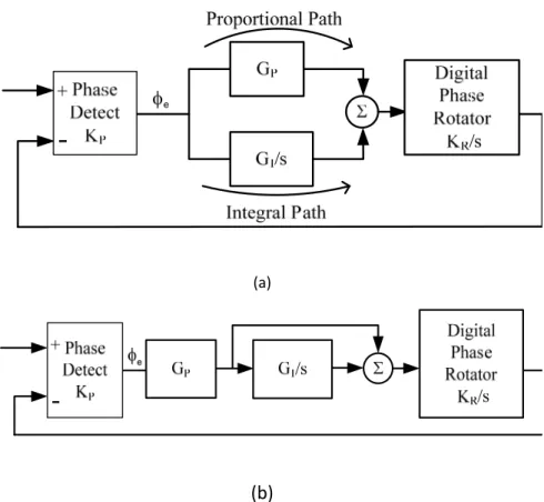
Fig. 3. 1 (a) The concept of 2nd‐order CDR. (b) The proposed 2nd‐order CDR.
The s-domain concept of 2nd-order CDR can be seen in Fig. 3. 1(a), the binary phase detector detects the phase difference φe, then φe is proportionally counted with a
gain GP, and integrated with gain GI. The ratio of the phase adjustments from the
proportional path to that from the integral path is defined to be the stability factor ξ [25]. In Fig. 3. 1(a), the stability factor equals GP/ GI. In binary phase detection
without deadzone, ξ should be greater than two times the loop latency in UI to achieve unconditionally stable [25]. However, in our design this constrain may be relaxed because the deadzone from M-AES as will be described in Section 4.2.1.
The results from two paths are summed and is used to direct the digital phase rotator. The rotator acts as the VCO in s-domain, which is an integrator of filter output, it integrates the phase +/- information and adjust the phase of sampling edges.
In our proposed architecture, however, in order to reduce hardware overhead in implementing integral path while maintaining loop stability, the arrangement is modified as in Fig. 3. 1(b). In Fig. 3. 1(b), the ξ now equals 1/GI. It can be shown in
s-domain analysis that if the natural frequency and damping factor of original 2nd-order CDR is n and ζ (different from ξ), then the proposed 2nd-order CDR will
have ω′ ω G
P and ζ′ ζ/ GP. Because the actual required phase adjustments
are very rare comparing to the phase detection results, the GP is less than 1, so the
natural frequency is reduced and damping factor is increased. Therefore parameters can be designed accordingly without changing loop characteristic. The implementation of GI, which is also less than 1, needs not to be so small therefore
requires less hardware (will be further explained in Section 3.2.3).
3.2 Phase/Frequency tracking CDR
The block diagram of the proposed feed-forward phase adjusted CDR is shown in Fig. 3. 2. At data rate fs=6GHz, a reference clock of 100MHz is given to the PLL to
generate a clock with 1.2GHz, 10 phases. Phase selection block, controlled by the digital 2nd-order algorithm, selects 5 phases for data sample and 5 phases for edge sample that tracks incoming stream with phase resolution of 1/32 UI. At the sampler, the incoming stream is sampled and synchronized with parallel 5-bits at 1.2GHz, equivalent to 6GHz data rate. The Phase Detector is a binary (bang-bang) [25] detector, that extract the phase lead/lag information from the data and edge samples. Then a Pre-Filter which composed of a majority vote and a sliding window is used to average out the effect of random jitter and balance the loop gain in different data transition density. The sliding window operates at the rate to 600MHz and its output is
Fig. 3. 2 The block diagram of proposed CDR.
used in the Proportional and Integral Path.
The proportional path and integral path behaves like a 2nd -order digital loop filter that interpret the Up/Down into phase and frequency adjustment, then the Phase rotator and decoder controls the Phase selection block.
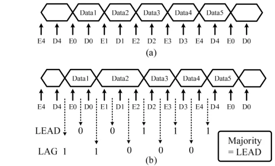
3.2.1 Pre-Filter
As shown in Fig. 3. 3 (a) and (b), the binary phase detection is done by exclusive-or the data sampling and edge sampling to detect transition and compare the transition with current clock edges. The Pre-Filter has a majority vote, which sums the 5 lead/lag signals and makes a final decision to represent current lead/lag, as shown in Fig. 3. 3 (b). This majority vote has two contributions: first, the effect of random jitter can be averaged, i.e., the randomness can be filtered out and the trend of phase
Fig. 3. 3 (a) The ideal operation of data and edge sampling. (b) Under jittery condition, the operation of binary PD and Pre‐Filter.
drifting can be maintained; second, the difference of data transition density often causes huge variation of loop gain and results in instability or loss of tracking. The majority vote can ensure an upper bounded gain when data transition is too often, and a minimum gain when data transition is too rare; hence preserve a reasonable loop gain.
The second part of pre-filter is the sliding window that changes the rate to 600MHz to enable later processing and produces the sum of two successive Pre-Filter outputs.
3.2.2 Proportional Path
The GP in Fig. 3. 1(b) is implemented by a modified first-order delta-sigma
modulator. The modification is done by adding sign bit path to handle both positive and negative inputs. The architecture and operation are shown in Fig. 3. 4. The input of proportional path is from sliding window that sums two successive Ups/Downs,
therefore is a 3-bit integer ranging from +2 to -2. The 3-bit is then extended to (N+1) bits for truncation. The value of proportional gain, GP, is decided by the truncation
depth N, that is, GP=2-N. For example, N=2 represents GP=0.25. In our design, the
depth N is programmable from 2 to 5.
In Fig. 3. 4 (b) and (c), we can see that when GP=1/4, in 6 cycle time,
proportional path generates 2 positive steps when input has 8 up signals, and 2 negative steps when input has 8 down signals. This implementation produce a time averaged gain equal to a fractional number, and the output is the phase adjustment step. The phase rotator will integrate the steps and tracks the incoming data phase. With the continuing of phase adjustment, the proportional also has a very limited frequency tracking capability. For example, in our proposed system, if N=3 is set, the proportional thpa has maximum frequency tolerance of
1 2N 600MHz 6GHz 1 32UI 390.625ppm (3. 1)
(a)
4
/
1
=
PG
(b)4
/
1
=
PG
(c) Fig. 3. 4 (a) The architecture of Proportional path. (b) The operation of Proportional path. (c) The operation with negative values.
Fig. 3. 5 The architecture of Integral path.
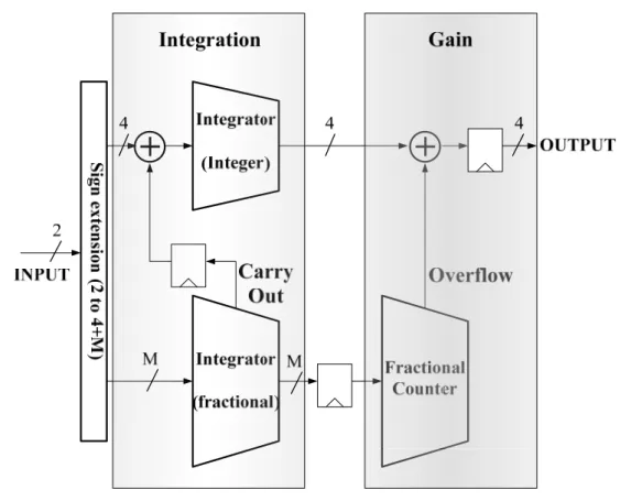
3.2.3 Integral Path
In order to track not only the phase but also frequency of incoming data, the Up/Down information must be integrated to form the frequency information. The integrated signal is then passed into a time averaged gain element similar to the proportional path, as shown in Fig. 3. 5. The input is extended to (4+M) bits, where 4-bits are integer part and M-bits are fractional parts. The integer width is determined by SSC spread frequency. When the maximum frequency deviation of SSC, the maximum phase adjustment of integral path is:
5000ppm 6MHz 6GHz 321
1
C 4 (3. 2)
in our design it is 0.5. The reason for choosing 0.5 as counter gain is explained in Section 3.2.4.
Being different from proportional path, the delay of integral path is not critical to jitter tolerance mask at high frequency. Therefore, pipeline insertion is suitable to maintain functionality at 600MHz. The pipelines are inserted between integer integrator, fractional integrator and fractional counter. As the proportional path, the integral gain GI is determined by the fractional depth M, that is, GI=2-M. Also the
length M in our design is programmable to be 4, 6, 8 or 10.
The benefit of placing integral path after proportional path instead of directly after sliding window can be explained. In a 2nd-order loop, it is important to keep the integral gain much smaller than the proportional gain, so that the integral path does not interfere with the proportional path and become unstable. For example, for a small stability factor ξ=128 and GP=1/8; if the integral path is directly after sliding window,
then we need GI=1/1024, which means M=10; but if the integral path is after
proportional path, then GI=1/ξ and M=7. Thus a smaller adder is required and timing
constraint can be easily achieved.
3.2.4 Phase Rotation Counter and Decoder
The Phase rotation is implemented by a 0-159 counter. The counter can up counting or down counting and the range of 0-159 represents 160 phases, which is the 10 phases from PLL multiplied by the interpolation of 16 intervals. The counter has a counter gain, GC= (1/2) from one bit truncation in the LSB. The operation and benefit
of the truncation can be explained by a simplified example. Assume the phase detector output is a constant 1, which means up counting the phase is required. A simplified
proportional path and an integral path are shown in Fig. 3. 7 and Table 3. 1 lists the operations of two cases. Because there is only positive input, the negative sign bit can be ignored.
The constant input is multiplied by GP and P is the proportional output, then it is
integrated to be A. A is then multiplied by GI; whenever B overflows, the integral
output, I, becomes 1. Table 3. 1 compares the different Counter gain setting. In the left column, LSB of counter is not truncated so GC=1. In this case we can see there are 2
times that the counter adjusts 2 steps in one clock cycle. In the right column, LSB is truncated, so the counter adjust only when the accumulation of P and I exceeds 2. Note that in order to maintain the same loop gain, GP is increased to 1/2. In this case
there is no 2 step adjustment in one cycle, although the total phase adjustments are the same. As a result we can observe that the LSB truncation in counter effectively “scatters” the phase adjustments, distribute them in time domain, preventing them from being too concentrated. This is an advantage when CDR loop is locked, it enhances stability and reduce cycle-to-cycle jitter of recovered clock; also reduce the hardware to implement GP. The difference of intrinsic jitter under the same gain
I
G
PG
G
C Fig. 3. 7 a Simplified Proportional, Integral and Counter graph. Table 3. 1 The operation of different Counter gain. Clk # Gc=1, GP=1/4, GI=1/8 GC=1/2, GP=1/2, GI=1/8 C P I A B C P I A B 0 1 1 0 0 0 0 1 0 0 0 1 0 0 0 1 1 0 0 0 1 1 2 0 0 0 1 2 1 1 0 1 2 3 0 0 0 1 3 0 0 0 2 4 4 1 1 0 1 4 0 1 0 2 6 5 0 0 0 2 6 1 0 1 3 1 6 1 0 1 2 0 0 1 0 3 4 7 0 0 0 2 2 1 0 1 4 0 8 1 1 0 2 4 0 1 0 4 4 9 0 0 0 3 7 1 0 1 5 1 10 1 0 1 3 2 0 1 0 5 6 11 0 0 0 3 5 1 0 1 6 4 12 2 1 1 3 0 1 1 1 6 2 13 0 0 0 4 4 0 0 1 7 1 14 1 0 1 4 0 1 1 1 7 0 15 0 0 0 4 4 1 0 1 8 0 16 2 1 1 4 0 1 1 1 8 0 17 0 0 0 5 5 0 0 1 9 1 18 1 0 1 5 2 1 1 1 9 2 19 0 0 0 5 7 1 0 1 10 4Fig. 3. 8 The Multi‐Phase VCO and Phase selection Block.
3.3 Phase Selection
The use of phase rotator with phase interpolation in phase adjustment has been broadly used in modern development of high speed CDRs [16]-[17][18], [34]-[39]. The Phase Selection block consists of phase multiplexers and phase interpolators. Of the 10 phases from PLL, the phase multiplexers choose two nearby phases for to interpolate into 16 intervals for finer resolution. As shown in Fig. 3. 8, due to the parallel 5-bit sampling of incoming data, the 5 data sampling and 5 edge sampling must be parallel shifted; therefore we need 5 duplications of multiplexer pair and interpolator.
multiplexer in the interpolated signal, a special phase multiplexing is used. As shown in Table 3. 2, we use a zigzag phase selection order instead of one-way selection. Each multiplexer has only even or odd phases as its inputs; therefore we need only 5-to-1 multiplexer but not 10-to-1s. The control signals of interpolator, N and N’, are complementary and switch the current source between the two inputs of interpolator, INT_A and INT_B. The detailed operation is as follows (
Table 3. 2):
When the phase moves from number 0 to 15, the MUX_1 selects P0 into INT_A and MUX_2 selects P1 into INT_B, and N and N’ gradually shift the current weighting from INT_A to INT_B. When number 15 to 16, the MUX_1 selects P2, meanwhile the interpolator current is all shifted to INT_B, therefore the switching of MUX_1 does not affect the interpolator output, and the glitch is avoided. After phase 16, the control of INT_A and INT_B is interchanged so that N and N’ shifts the weighting from INT_B to INT_A. This zigzag order works for both forward and backward rotation. The phase selection circuits achieves 160 phase interpolation of a 1.2GHz clock, equivalent to 1/32 UI of 6Gb/s data rate.
Table 3. 2 The operation of phase selection
3.3.1 Phase Multiplexer
The 5-to-1 phase multiplexer is shown in Fig. 3. 9 (a). The control signal S0-S4 selects one of the inputs IN0-IN4. The bias voltage of Bias_PMOS and Bias_NMOS are provided by a replica bias generator that similar to that used in VCO delay elements in PLL [26]. P Phhaassee n nuummbbeerr Phase
Phasemultiplexmultiplex IInntteerrppoollaattiioonn
Contr
Control & directionol & direction
MUX
MUX_1_1 MUX_2MUX_2 IINNTT__AA IINNTT__BB
0 0--1155 PP0 0 P P11 N N’’>>>>>>N N 1 166--3311 P P2 2 N N<<<<<<NN’’ 3 322--4477 P P33 N N’’>>>>>>NN 48-63 48-63 P P4 4 N N<<<<<<NN’’ 6 644--7799 P P55 N N’’>>>>>>NN 8 800--9955 P P6 6 N N<<<<<<NN’’ 9 966--111111 P P77 N N’’>>>>>>NN 1 11122--112277 P P8 8 N N<<<<<<NN’’ 1 12288--114433 P P99 N N’’>>>>>>NN 1 14444--115599 pp0 0 NN<<<<<<NN’’
(a)
(b)
Fig. 3. 9 (a) The Phase Multiplexer (b) The Phase Interpolator
Fig. 3. 10 The Data sampler (a) Comparator (b) Amplifier/Latch
3.3.2 Phase Interpolator
The phase interpolator is shown in Fig. 3. 9 (b). The control signal N0-N12 is thermal coded to ensure monotony of phase selection. The bias voltages are also provided by replica bias generator.
3.3.3 Data sampler
The data sampler is shown in Fig. 3. 10. The first stage of sampler is a comparator. When the clock is low, both Out+ and Out- are reset to high, In+ and In- are stored in the capacitance and the latch is turned off; when clock rises, the latch begin to regenerate the Out+ and Out-. The second stage acts as an amplifier when clock is high and reduce metastability; when clock is low, because both Out+ and Out- are high, the value is latched by internal back-to-back inverter pair and the timing margin for synchronization of Data+ and Data- can be increased.
3.4
Simulation Results
3.4.1 Behavior Modeling
The behavior of the CDR can be modeled with a discrete-time closed-loop system. Fig. 3. 11 shows a conceptual model. There are three gain parameters that are tunable to fit jitter specifications. They are phase-rotator counter gain KR,
Proportional gain GP and Integral gain GI. In general, KR=1/2 is set as mentioned in
section 3.2.4. The z-n models the total loop delay. The loop delay directly affects loop stability and jitter performance and should be carefully designed to minimize it.
The detailed MATLAB model is shown in Fig. 3. 12. Using this model, GP and
GI can be designed according to the simulation results. The simulation of transient
response of varies types of jitter includes phase step, random jitter, periodic jitter, ISI, frequency offset and spread spectrum clock.
From the simulation results we can see that the jitter tolerance is directly determined by the response of proportional path. A large gain GP results in higher loop
bandwidth to track higher frequency jitter. However, large GP makes the loop more
1 1− z− KR 1 1− z− GI 1 −
z
nz
−G
P inφ
outφ
4 3 2 1 1 − − − − + + + + z z z z Fig. 3. 11 The discrete‐time model of the proposed CDR.sensitive to random jitter and induces larger oscillation in steady state; fortunately, the effect is reduced by the majority voting and the LSB truncation of phase-rotator counter. In Fig. 3. 13, we simulate the high frequency corner of jitter tolerance mask specified in section 2.3.2 and the conditions are summarized in Table 3. 3. We can see that when GP is large, jitter mask can be met; when GP is small, slewing occurs and
CDR cannot meet input jitter mask.
In the other hand, the integral path provides low frequency phase tracking as well as tracking of frequency offset and spread spectrum. As shown in Fig. 3. 14, the tracking in Fig. 3. 13 (b) that results in skew is aided by a larger integral path gain (GI
= 1/64) and provides better response. However, large GI reduce stability factor and
Fig. 3. 12 The det ail MA TL AB model of CD R .
(a) (b)
Table 3. 3 Summary of Fig. 3. 13. Fig. 3. 13. GP PJ Frequency (Hz) PJ Amplitude (UI p-p) (a) 1/8 400K 1.6 (b) 1/16 400K 1.6 (c) 1/8 1M 0.8 (d) 1/16 1M 0.8 (e) 1/8 4M 0.2 (f) 1/16 4M 0.2 Note: GI =1/256, RJ: σRJ=0.02UI Fig. 3. 14 Simulation of Fig. 3. 13(b) with GI = 1/64
The integral path is designed to accommodate frequency offset and spread spectrum clock. With the aid of integral path, the frequency tolerance is enhanced to 1000ppm; and the spread spectrum clock of 5000ppm deviation, 33KHz modulation frequency can be tracked. Fig. 3. 15 and Fig. 3. 16 show the simulation results of SSC tracking. Fig. 3. 15 shows the phase adjustments made by phase rotator to track SSC in one period of modulation. Fig. 3. 16 shows the phase tracking error in the presence of high frequency periodic jitter, using specifications in the high frequency corner of
jitter tolerance mask; all of them using GP=1/8, GI=1/64 setting.
It can be seen that the periodic behavior of tracking error reflects the input jitter pattern, but the error is still well under 0.15 UI, thus satisfies the tolerance mask requirements.
From the above simulation results, we set the parameters of GP and GI
programmable for different jitter conditions. GP is selectable from 1/4, 1/8, 1/16, 1/32;
and GI is selectable from 1/16, 1/64, 1/128, and 1/1024 for no SSC application. In
general, from the simulation results, GP=1/8 and GI=1/64 or 1/128 should be a proper
configuration that tracks high frequency PJ and SSC while maintaining good stability. The simulated jitter tolerance mask with STM-64 specification in GP=1/8 and
GI=1/64is shown in Fig. 3. 17.
Fig. 3. 15 Phase adjustments in one SSC modulation period.
(a) (b) (c) Fig. 3. 16 Phase tracking error in SSC&PJ simulation (a) SSC + 400KHz, 1.6 UI(p‐p) (b) SSC + 1MHz, 0.8 UI(p‐p) (c) SSC + 4MHz, 0.2 UI(p‐p)
1.0E‐01 1.0E+00 1.0E+01 1.0E+02 1.0E+03 1.0E+04 1.0E+05
1.0E+00 1.0E+01 1.0E+02 1.0E+03 1.0E+04 1.0E+05 1.0E+06 1.0E+07 1.0E+08
Amplitude (UI p ‐p) Frequency (Hz) Simulation Results STM‐64 Jitter Tolerance Mask Fig. 3. 17 Simulated Jitter tolerance mask.
3.4.2 Circuits Simulation
The circuit level simulation is performed using mixed-mode simulator in Nanosim. In the simulation, GP=1/8 and GI=1/64 and this is to ensure larger jitter
tolerance to verify functionality.
The input pattern is K28.5 which is a DC-balanced pattern and includes 5 successive ‘1’s and ‘0’ and successive transition ‘01010’, ‘10101’ to test ISI effect. The K28.5 is ‘10100 00011 01011 11100’ and starts from LSB.
To verify the CDR function, a built-in-self-test (BIST) circuit is used. The BIST will automatically parallelize and align the serial input, and detect the K28.5 pattern. After the K28.5 is found, the signal bus ‘rev_data’ displays the pattern and the signal ‘data_en’ is set high. If bit error occurs, ‘rev_data’ no longer shows K28.5 pattern and ‘data_en’ is set low.
over-designed the circuit and simulate it at a faster rate of 6.945Gb/s instead of 6Gb/s. That means the local PLL generates 1.389GHz instead of 1.2GHz.
The simulation of sampler circuits is shown in Fig. 3. 18. The clock is set at 1.6GHz, 40ps rise/fall time corresponding to the simulation result of sampling clock; the receiver data rate is 8Gb/s with 200mV swing after 10M cable model.
To test spread spectrum clock functionality, the receiver local clock generator is a spread-spectrum clock generator that generates -5000 ppm, 33KHz modulation frequency SSC. The receiving data is sent at nominal rate, therefore the CDR has to recover the nominal data rate to produce correct data. The simulations result is shown in Fig. 3. 19. The simulation is taken for one modulation period, and the ‘rev_data’ signal shows the K28.5 correctly for the whole period.
The phase rotation of sampling clock is shown in Fig. 3. 20 and Fig. 3. 21. Fig. 3. 20 shows the phase rotation of 160 phases of sampling clock, which includes 10 groups of 16-phase interpolation. It can be seen that there are small gaps between groups, which is shown in Fig. 3. 21.
Fig. 3. 22 shows the recovered clock jitter in a non-SSC simulation. The simulated pattern contains only random jitter of σRJ 0.02UI. The peak-to-peak jitter is 17.516ps.
Fig. 3. 23 shows the clock spectrum in a SSC simulation. The receiver clock is from the local spread spectrum clock generator, and the recovered clock is from the received data transmitted at nominal rate and divided by 5. It can be seen that the data clock is recovered from the spread spectrum local clock and is at 1.389GHz.
Fig. 3. 18 Simulation results of sampler circuit. (a) (b)
Fig. 3. 20 The rotation of 160 phase.
Fig. 3. 22 Recovered clock jitter in non‐SSC simulation.
Table 3. 4 CDR simulation summary
Process 90nm CMOS (1.0V supply)
Speed 6 Gb/s Power (mW) CDR digital CDR analog SSCG&PLL 6 41 8 Active Area (mm2) CDR digital CDR analog SSCG&PLL Loop filter 0.22*0.32 0.24*0.38 0.24*0.18 0.27*0.22 Recovered Clock
Jitter 54.420ps 17.516ps PJ, Amp=0.18UI(p-p), Freq=1MHz RJ, σ=0.02UI Freq Tolerance +/- 1000 ppm
Chapter 4
Multiple Alternating Edge Sampling
(M-AES) Scheme
4.1 Overview
The binary phase detection (Bang-Bang detection) has become the mainstream in phase detect method in modern high speed CDR circuits. It has many advantages over traditional linear phase detectors [25]. For example, it can be implemented by the flip-flops; therefore the circuit can operate at the speed where a process technology is able to build flip-flops. The detector then will not limit the operating speed for a given process. Another advantage is that the binary phase detector generates phase information in simple digital values. This enables the processing of multi-phase sampling structures. Therefore, the CDR can operate in parallel multi-phase operation when the required bit rate exceeds the process capability to build a full rate phase
detector.
However, the binary phase detectors have some undesired nature that cause the degradation in tracking behavior and jitter performances. The most obvious disadvantage is that it provides only binary (lead/lag) or ternary (lead/lag/hold) phase information, but no quantity of phase deviation. The nonlinear nature results in oscillation when phase locked, thus generates intrinsic jitter in steady state [34] [35].
Another disadvantage of binary PD is that its PD gain varies greatly with different jitter conditions [19]. The binary detection of a jittery input creates a large PD gain when jitter is small and a small PD gain when jitter is large. This further deteriorates the stability of phase detection. The binary PD also has limitation when facing asymmetric jitter distributions [20]. In the presence of deterministic jitter such as inter symbol interference (ISI) or duty cycle distortion, the distribution of jitter is often asymmetric and biased in one direction. The traditional binary PD tends to lock on to the point that equally divides the area of distribution, i.e. the 50% probability point; while the best sampling point that produces least BER is at the midpoint between the edges of distributions.
Overall, the drawbacks of binary PD come mainly from its nonlinearity. Therefore it is most desirable to create a “linear” nature out of the binary PD. Due to the parallel sampling that used in our CDR, we can take advantage from the multiple-phase sampling and modify the sampling mechanic to improve the linearity while still using binary phase detectors. This is the concept of Multiple Alternating Edge Sampling.
4.2 Edge sampling schemes
4.2.1 Proposed M-AES Scheme
To overcome the drawbacks from binary PD, many good edge sampling schemes are proposed [19][20][34][35]. [19][20] overcame PD gain variation and asymmetric jitter distribution by introducing an adaptive deadzone. [34][35] reduced intrinsic jitter caused by oscillatory steady state of binary PD, by introducing dithering in interpolator control signal and creating variation of edge sampling position. However, both the above methods are not suitable for our application. First, adaptive deadzone in [19][20] are analog implementation using PLL tracking type CDR, which is not a dual loop CDR that benefits from bandwidth relaxation. Also the effect of asymmetric jitter presents only under large jitter conditions (σRJ>0.06UI) which is beyond the SATA specification. Furthermore, the adaptive deadzone has difficulty in discriminating large periodic jitter or frequency offset from ordinary ISI, hence isn’t appropriate for SSC applications. Second, the dithering of edge sampling signal in [34][35] requires different interpolator control for data sampling and edge sampling, this requires huge amount of circuit complexity especially in multi-phase parallel sampling CDR that uses multiple interpolators.
We therefore propose an edge sampling scheme to linearize PD gain and it is suitable for digital implementation using simple circuit design. The concept is explained below and the implementation is described in section 4.3.
The proposed Multiple Alternating Edge Sampling is shown in Fig. 4. 1.Unlike the 3x oversampling that uses two edge samplings per UI in [20], one edge sampling altering at two sides of original point is enough to create deadzone. Furthermore, because we have five parallel bit sampling, we can alternate the five edge sampling clock E0 ~ E4, each to different amount of phase. This equivalently creates eleven different levels of PD gain proportional to the phase deviation. (In the presence of Majority Vote, in order to restrict intrinsic jitter, the middle point E2 must include the effective gain times loop latency, which is the intrinsic jitter amount. In our design the
Fig. 4. 1 The proposed Multiple Alternating Edge Sampling Fig. 4. 2 Phase step track (a) w.o. AES (b) w.i. AES.
altering amount are chosen to be (0.04/0.06/0.08/0.10/0.12)UI where 0.08UI contains the intrinsic jitter.) The comparison of PD output and phase step response between original PD and AES PD is shown in Fig. 4. 2. It can be seen that while original PD creates large intrinsic jitter, AES PD locks within a small deadzone which equals 2*E0.
4.2.2 Edge sampling schemes and PD output
In this section we compare different edge sampling schemes: traditional 2X oversampling (binary PD), 3X oversampling (two edge sampling per UI), multiple 3X oversampling (two edge sampling per UI with multiple spreading), and the proposed multiple alternating 2X oversampling. We also study their phase detection behavior. We compare three different jitter sigma conditions, they are σRJ=0.002, 0.03, 0.1,
respectively, as shown in Fig. 4. 3.
Fig. 4. 4 (a) shows the PD output of 2X oversampling. We can see that the PD gain varies greatly for different jitter and tends to be unstable. Fig. 4. 4 (b) shows the PD output of 3X oversampling. The two edge sampling is at +/- 0.1UI away from original point and creates a deadzone of 0.1UI.Fig. 4. 4 (c) shows the PD output of multiple 3X oversampling. The two edge sampling is spread from original point (0.04/0.06/0.08/0.10/0.12)UI away to both directions. We can see that the PD output is more linearized. Fig. 4. 4 (d) shows the PD output of multiple alternating 2X oversampling. The one edge sampling is alternating between two directions and spreads from original point (0.04/0.06/0.08/0.10/0.12)UI away. It can be seen that the PD output is almost identical to the multiple 3X oversampling scheme. This means that we do not need to waste more circuitry to generate two edge sampling per UI, but the same linearization of PD output can be acquired.
Fig. 4. 3 Different jitter sigma conditions for comparison of PD output. (a) (b) (c) (d) Fig. 4. 4 The PD outputs for different edge sampling schemes. (a) 2X oversampling. (b) 3X oversampling. (c) Multiple 3X oversampling. (d) Multiple alternating 2X oversampling.
4.2.3 Edge sampling schemes and Jitter performance
In this section we evaluate the jitter performance and BER of different edge sampling schemes using MATLAB and Mathematica. We like to evaluate which sampling scheme gives the best sampling point under different jitter conditions, especially asymmetric jitter distributions. The method of calculating BER is relatively simple: First we find out where will each sampling scheme places its sampling point with respect to the jitter distribution. Then we calculate the BER corresponding to each sampling point and summation. The detail is shown in Fig. 4. 5.In order to find out the sampling point, we must note that the sampling point is not stationary. Instead, it may be drifting due to the oscillatory nature of binary PD, or from the randomness of jitter. However, we can calculate its histogram, by using MATLAB to model each of the above sampling schemes under different jitter conditions and record the corresponding distribution of sampling point. The histogram is discrete with (1/32) UI spacing. In modeling, GP is 1/16 and GI is 1/256.
After finding the histogram of sampling point, we calculate the BER corresponding to the histogram. The histogram is flipped around centered at y-axis,
Data jit ter Probability Convolution 0 0.1 0.2 0.3 0.4 0.5 0.6 ‐2 ‐1 0 1 2 Samplin g histogram Flip ped arou nd
Fig. 4. 6 The asymmetric jitter conditions.
and normalized to summation of 1. Then it is convoluted with the jitter distribution, to represent the total jitter amount seen by every tone of the histogram. Then the area of distribution deviating more than 0.5 UI from the origin is integrated as the BER. In this modeling, we not only considered the static sampling point with respect to asymmetric jitter, but also take into account the intrinsic jitter from the loop dynamic in different sampling scheme and jitter condition. Therefore the BER can be more realistic in representing the performance of different edge sampling schemes.
The analysis is composed of four different asymmetric jitter conditions(Fig. 4. 6):
Case 1: w1=0.0 UI, a1=0.7; w2=0.06 UI, a2=0.3; σ1=σ2=σ. Case 2: w1=0.0 UI, a1=0.7; w2=0.12 UI, a2=0.3; σ1=σ2=σ.
Case 3: w1=0.0 UI, a1=0.7; w2=0.06 UI, a2=0.3; σ1=σ, σ2=(1.5)σ. Case 4: w1=0.0 UI, a1=0.7; w2=0.18 UI, a2=0.3; σ1=(0.7)σ, σ2=σ.
The 4 cases represent different degrees of ISI or duty cycle distortion, and we simulate the cases with σ= (0.02, 0.06, 0.10) to see the effect of jitter severity. The jitter distribution for each case and the resulting PD output for each sampling scheme are shown in Fig. 4. 7 to Fig. 4. 10, and the calculated BER are summarized in, Table 4. 1, Table 4. 3, Table 4. 3, Fig. 4. 12, Fig. 4. 13 and Fig. 4. 13..
![Table 2.1 Generations of SATA [29]](https://thumb-ap.123doks.com/thumbv2/9libinfo/8742967.204487/34.892.209.766.824.1100/table-generations-of-sata.webp)