國 立 交 通 大 學
電子物理研究所
博 士 論 文
週期性分散式砷化鋁鎵銦多量子井的光學特性:
自發輻射、受激輻射及飽和吸收特性
Optical Properties of the Periodically Distributed AlGaInAs
Multiple-Quantum-Wells: Spontaneous Emission, Stimulated
Emission and Saturable Absorption
研 究 生:陳毅帆
指導教授:陳永富 教授
週期性分散式砷化鋁鎵銦多量子井的光學特性: 自發輻射、受
激輻射及飽和吸收特性
Optical Properties of the Periodically Distributed AlGaInAs
Multiple-Quantum-Wells: Spontaneous Emission, Stimulated Emission and
Saturable Absorption
研 究 生:陳毅帆 Student:Yi-Fan Chen
指導教授:陳永富 Advisor:Yung-Fu Chen
國 立 交 通 大 學
電 子 物 理 學 系
博 士 論 文
A DissertationSubmitted to Department of Electrophysics College of Science
National Chiao Tung University in partial Fulfillment of the Requirements
for the Degree of Doctor of Philosophy
in Electrophysics
June 2013
Hsinchu, Taiwan, Republic of China
週期性分散式砷化鋁鎵銦多量子井的光學特性:
自發輻射、受激輻射及飽和吸收特性
學生 : 陳毅帆
指導教授 : 陳永富
國立交通大學電子物理學系博士班
摘 要
週期性排列的半導體多量子井結構作為半導體雷射的增益介質上相較於傳統 的異質結構具有波長可調、低激發放射的閾值及較好的載子侷限特性。而相較於 離子摻雜的晶體,其作為被動式Q 開關固態雷射的飽和吸收體上也具有非飽和損 失較小及作用長度極短的優點。結合以上特性半導體多量子井結構很有潛力作為 一個同時進行飽和吸收及波長轉換的光學元件。此外由其近似二維的量子侷限結 構加上高強度的激發使得受激載子間的多體效應相當顯著。因此本論文架構基本 上可分為三個部份,第一部份首先討論高濃度電子電洞對在近似二維侷限的多量 子井結構下展現的多體效應,藉由較高的侷限能障及週期性排列的多量子井結構 我們觀察到了常溫下重整化能隙的自發輻射頻譜,相較於過去文獻僅對此輻射頻 譜作不同受激載子濃度下的探討,我們對此多體效應下新發生的能態對溫度的頻 譜變化及輻射頻譜的集成強度作詳細的探討,並配合其發生的閾值強度隨溫度增 加指數提升的結果驗證了週期性的多量子井結構對常溫下重整化能態自發輻射頻 譜的觀察的重要性。 在了解了高激發強度下多量子井結構的螢光特性後,本論文的第二部份則是 實現以砷化鋁鎵銦多量子井結構作為光激發半導體雷射的增益介質。首先藉由掺峰功率光激發半導體雷射,在脈衝頻率及寬度可調的激發光源下可優化最佳的雷 射輸出條件。接著在相同的激發光源下將同樣砷化鋁鎵銦半導體多量子井結構設 計在光通訊及人眼安全波段以得到1520 nm 的高重覆率及高尖峰功率光激發半導 體雷射輸出,其中經由高透明度及高熱傳導率的單晶鑽石散熱片與半導體增益介 質的鍵合技術解決了高重覆率及高激發功率下的熱反轉現象,使得最佳雷射操作 重覆率從30 kHz 提升到 200 kHz 且最高平均功率輸出提升了 4.7 倍,即使將重覆 率提升到500 kHz 仍有 2.32 W 的平均功率及 170 W 的尖峰功率輸出。 本論文最後一部份則是利用設計在1530 nm 的砷化鋁鎵銦多量子井結構同時 作為1064 nm 掺釹釩酸釔固態雷射的飽和吸收體及波長轉換元件,其多量子井結 構 n=2 的能階提供1064 nm 的非線性飽和吸收作用而 n=1 的能階搭配適當耦合共 振腔則可進行增益轉換產生1530 nm 的脈衝雷射輸出,此一架構結合了自調 Q 雷 射、腔外脈衝式幫浦雷射及半導體多量子井結構的優點,由於被動式Q 開關不需 額外電子驅動元件且和受掺離子晶體飽和吸收體及非線性晶體相比量子井結構的 作用長度相當短可縮減腔長,因此若搭配第二部份所述不同介質間的鍵合技術其 相當具潛力作為低成本、簡單、一體成形且波長可設計範圍廣的微片被動式調 Q 雷射。
Optical Properties of the Periodically Distributed AlGaInAs
Multiple-Quantum-Wells: Spontaneous Emission, Stimulated
Emission and Saturable Absorption
Student : Yi-Fan Chen
Advisor : Yung-Fu Chen
Department of Electrophysics
National Chiao Tung University
ABSTRACT
Recently, the semiconductor multiple-quantum-wells (MQWs) structure is extensively used in the semiconductor lasers owing to the characteristics like versatile emission wavelength, lower laser threshold and excellent performance under room temperature operation. It is also applied as a promising saturable absorber in the diode-pumped passively Q-switched solid-state laser. Compared to the doped crystal saturable absorber, the MQWs absorber has lower non-saturable loss and allows the shorter cavity length. According to these characteristics, the MQWs structure has the potential to be designed simultaneously as a saturable absorber and an active medium in the intra-cavity pumped solid-state lasers. Besides, the many-body effect of the high density electron-hole plasma (EHP) under this quasi-2D confinement structure is also an interesting issue. Therefore, the contents of this dissertation are organized to be three parts. At the first part we investigate the many-body effect of the high density EHP in the quasi-2D confined MQWs structure. The room temperature spontaneous emission of the renormalized bandgap is observed under the designation of high confinement energy and periodically aligned gain structure. The temperature dependent luminescence
discussed and the threshold excitation intensity of the luminescence of renormalized band-edge is shown to be exponentially increased with increasing temperature. As a result we have confirmed that the periodically aligned MQWs structure is beneficial to the observation of room temperature many-body state emission
In the second part, an AlGaInAs MQWs structure is designed to be the gain chip of a high repetition rate and high peak power 1220 nm optically-pumped semiconductor laser (OPSL). By using an Yb-doped master oscillator fiber amplifier as the pump source, the output performance could be optimized with the free controlled pump conditions such as pump repetition rates and pulse durations. Then the same pump laser is used to excite the high repetition rate and high peak power AlGaInAs MQW OPSL at the communication and eye-safe spectral region of 1520 nm. By capillary bonding the highly transparent and thermal conductive single crystal diamond heat spreader to the gain chip, the thermal roll-over effect was eased at high average pump power under high repetition rate operation. The optimized repetition rate was raised from 30 to 200 kHz and the maximum average output power was scaled to be 4.7 times higher. When operated at as high as 500 kHz, the maximum average power of 2.32 W and peak power of 170 W were obtained.
At the end of this dissertation an AlGaInAs MQW structure is used simultaneously as the saturable absorber (SA) and wavelength-converted component in the Nd:GdVO4 laser. It is fabricated to accommodate the pump level of 1064 nm and the emission level of 1530 nm in the quantum well region. The upper state is served as the nonlinear saturable absorption device at 1064 nm and the lower state is served as the active medium at 1530 nm with additional couple-cavity in the Nd:GdVO4 laser. This configuration combines the advantages of the self-Q-switched lasers, pulse-pumped solid state lasers and the semiconductor MQW structures. Because there is no need of additional electronic drivers for passively Q-switches and the shorter action lengths of the MQWs compared to the bulk crystal SAs and nonlinear crystals, the device configuration could be simplified and cavity length is shortened, respectively. According to these characteristics and the capillary bonding technique in second part, this laser system has potential to be served as a low cost, simple and monolithic passively Q-switched microchip laser with broad achievable spectral range.
誌
謝
能完成這份博士論文及學位有許多需要感謝的對象,首先我最需要感謝的是 我的指導老師-陳永富教授,陳老師除了指引我學習及研究的方向之外其在課堂上 的教誨也讓我建立了立身處世的原則,其次要感謝的是黃凱風教授,除了提供實 驗中最重要的半導體樣品外,黃老師對於我的研究也提供了許多想法及意見,而 作為共同指導的蘇冠暐助理教授則是教導了我在研究上許多的基礎知識和經驗, 而對於我許多想法上的反饋也促使我建立了邏輯性的思考。接著我想要感謝我的 父母,除了生育養育我以及不辭辛勞的付出之外,自小至大對我的人格的培育有 無可比擬的重要性,並且容忍及支持我人生中如此長的求學生涯,因此我每每思 其恩德均不敢或忘。 除了師長及父母的影響之外,在研究所這段求學生涯中也受到實驗室許多同 仁的幫助,在這裡感謝張漢龍博士指導我半導體雷射的概念、黃仕璋博士教導我 架腔等實驗裝置的基礎、江柏毅學長提供我實驗上許多電子裝置的支援以及余彥 廷博士和段必輝學弟協助我完成低溫下重整化能隙自發輻射頻譜的量測,也感謝 其他同仁在實驗上及生活上提供的大大小小的協助。最後要感謝的是政府及學校 單位在網路、書籍及設施等資源上的提供以及國科會在實驗經費及個人工作費上 的補助。
Contents
Abstract (Chinese) ………...…….. i
Abstract ………...….. iii
Acknowledgement ………...….. v
Contents ………...…….. vi
List of Figures ………...……….. viii
List of Tables ………...……….. xii
Chapter One Introduction………...………… 1
1.1 Semiconductor gain materials………. 1
1.2 Spontaneous emission of multiple-quantum-wells…...…...…………... 7
1.3 Optically-pumped semiconductor lasers …………..……….……. 11
1.4 Semiconductor saturable absorbers………...……...…………... 15
Reference ………. 20
Chapter Two Spontaneous Emission Properties of the AlGaInAs Multiple-Quantum-Wells under High Excitation Intensity……..…….……... 31
2.1 Device fabrication of the AlGaInAs multiple-quantum-wells…...……. 31
2.2 Experimental setup………...………..………. 35
2.3 Experimental results and discussions………...…………..………. 44
2.4 Conclusions………...………..…… 53
Reference ………. 55
Chapter Three High-Peak-Power and High-Repetition-Rate 1.2-1.6 μm Optically-Pumped Semiconductor Lasers………..……….… 58
3.1 Thermal managements of the optically-pumped semiconductor lasers.………..…… 58
3.2 1220 nm AlGaInAs multiple-quantum-wells lasers………….……..… 63
3.2.1 Device fabrication and experimental setup……….………... 65
3.2.2 Experimental results and discussions………...………... 67
3.3 1520 nm AlGaInAs multiple-quantum-wells lasers………….……..… 75
3.3.1 Device fabrication and experimental setup……….……... 78
3.3.2 Experimental results and discussions………... 81
3.4 Conclusions………. 89
Reference ………. 89
Chapter Four Simultaneous Q-switching and Wavelength Conversion of the AlGaInAs Multiple-Quantum-Wells……….…. 96
4.1 Simultaneously passively Q-switched and frequency-switched behaviors of the multiple-quantum-wells...……… 96
4.2 Device fabrication and experimental setup……….…...…...…….. 99
4.3 Experimental results and discussions………...…………..………. 103
4.4 Conclusions………...………..…… 111
Reference ………. 111
Chapter Five Summary and Future Works………...…..……….. 116
5.1 Summary………...………..……… 116
5.2 Future works………...………..……….. 117
Reference ………. 120
Curriculum Vitae ……… 122
List of Figures
Chapter One
Fig. 1.1-1 Schematic illustration of the structure of edge-emitting laser………… 3 Fig. 1.1-2 Schematic illustration of the structure of surface-emitting laser……… 4 Fig. 1.3-1 The typical gain mirror configuration of the OPSLs……….. 14 Fig. 1.4-1 The pulse formation processes of typical passively Q-switched lasers.. 18 Fig. 1.4-2 Typical device structure of A-FPSA used in the passively Q-switched
microchip laser……… 19
Chapter Two
Fig. 2.1-1 The diagrams of the MQWs structures with (a) weak and (b) strong
coupling of the light-QWs interaction……… 34
Fig. 2.2-1 Schematic diagram of the radiative recombination mechanisms of the AlGaInAs MQWs in the simplified single QW configuration………... 36 Fig. 2.2-2 Room temperature transmittance spectrum of the AlGaInAs MQWs
chip excited at low intensity………... 37
Fig. 2.2-3 Room temperature reflectence spectrum of the AlGaInAs MQWs chip
excited at low intensity………... 38
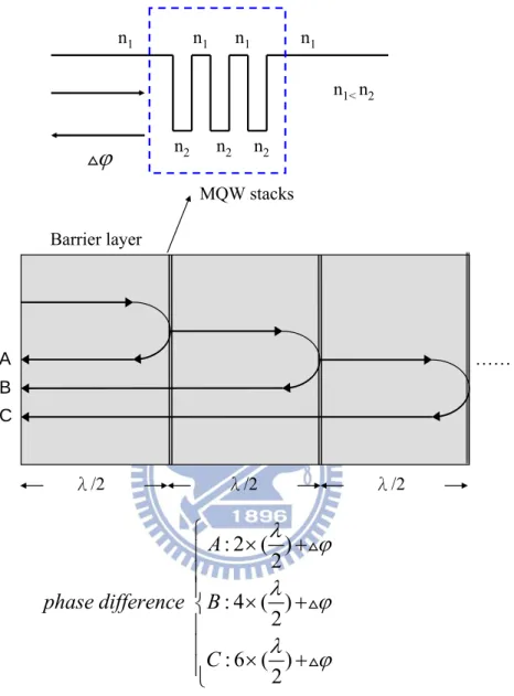
Fig. 2.2-4 Schematic illustration of constructive interference of waves A, B and C which are reflected from interfaces of three stacks of MQW
structure………...40
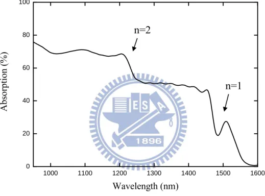
Fig. 2.2-5 Room temperature absorption spectrum of the AlGaInAs MQWs chip
excited at low intensity………... 41
Fig. 2.2-6 The experimental configuration of the PL spectrum measurement…… 43 Fig. 2.3-1 Photo-luminescence spectra of the AlGaInAs MQWs chip with
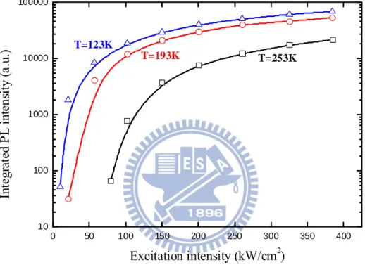
variance excitation intensity from 23 to 384 kW/cm2 at 253 K………..45 Fig. 2.3-2 Integrated PL intensity of the many-body state emission line as the
function of excitation intensity at 253, 193 and 123 K………... 46 Fig. 2.3-3 Photo-luminescence spectra of the AlGaInAs MQWs chip with the
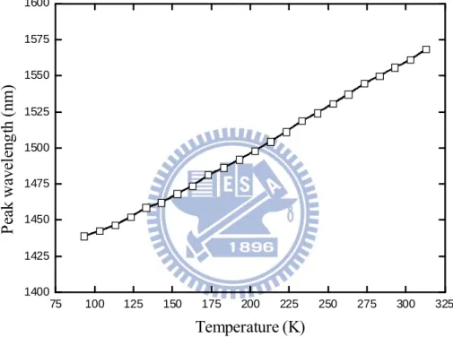
from 123 to 313 K………... 48 Fig. 2.3-4 Peak wavelength shift of the many-body state luminescence versus
temperature at the excitation intensity of 407 kW/cm2………...49 Fig. 2.3-5 Plots of the integrated PL intensity of the many-body state
luminescence versus temperature at the excitation intensity of 407
kW/cm2………... 51
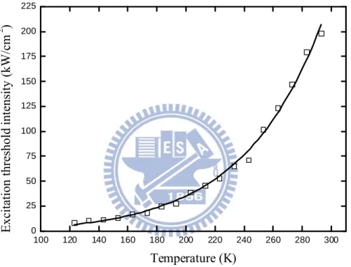
Fig. 2.3-6 Temperature dependence of the excitation threshold intensity of the
EHP renormalized state emission………... 54
Chapter Three
Fig. 3.1-1 The schematic illustrations of (a) barrier and (b) in-well pump
configurations of MQWs……… 61
Fig. 3.1-2 The schematic configurations of the two thermal management using (a) thin-device and (b) intra-cavity heat spreader methods……… 62 Fig. 3.2-1 Experimental configuration of AlGaInAs/InP semiconductor laser at
1200 nm pumped by a 1.06 μm Yb-doped pulsed fiber amplifier in the
single chip scheme……….. 66
Fig. 3.2-2 Room temperature surface emitting spontaneous emission spectrum under 60 kHz pump repetition rate and 28 ns pump pulse width at average absorbed power of 0.38 W. Inset, the expanded lasing spectrum obtained with 0.85 W average absorbed power under the
same pump conditions……….68
Fig. 3.2-3 Redshift of peak lasing wavelength as a function of average absorbed power under 60 kHz pump repetition rate and 28 ns pump pulse
width………... 70
Fig. 3.2-4 Laser output performances at fixed pump pulse width of 28 ns and different pump repetition rates ranged from 40-80 kHz………. 71 Fig. 3.2-5 Laser output performances under 60 kHz pump repetition rate with
varied pump pulse width………. 73
Fig. 3.2-6 (a) Typical oscilloscope trace of a train of pump and output pulses and
(b) expanded shapes of a single pulse……….74
Fig. 3.2-7 Output performance with double gain chips at 60 kHz pump repetition
Fig. 3.3-1 Experimental setup of AlGaInAs eye-safe laser at 1525 nm with an intra-cavity diamond heat spreader and using an Yb-doped pulsed
fiber amplifier as a pump source……….79
Fig. 3.3-2 Room temperature surface emitting spontaneous emission spectrum under a 100-kHz pump repetition rate at an average absorbed power
of 0.8 W……….. 82
Fig. 3.3-3 Output performances of the eye-safe laser without and with the diamond heat spreader at a 30-kHz repetition rate………. 83 Fig. 3.3-4 Output performances without (a) and with (b) the diamond heat
spreader for repetition rates in the range of 100-500 kHz……….. 85 Fig. 3.3-5 (a) Lasing spectrum with the heat spreader under an average absorbed
power of 2.5 W at a repetition rate of 100 kHz. (b) Dependence of the red-shift on the absorbed pump power for the laser operation without and with the heat spreader at a repetition rate of 100 kHz………..86 Fig. 3.3-6 (a) Oscilloscope trace of a train of pump and output pulses obtained
with an average absorbed power of 2.5 W at a repetition rate of 200 kHz. (b) Expanded shapes of a single pulse………... 88 Chapter Four
Fig. 4.2-1 Experimental configuration of the diode-pumped Nd:GdVO4 laser simultaneously passively Q-switched and frequency-switched by the
AlGaInAs/InP M.QWs……… 102
Fig. 4.3-1 Average output powers at 1064 nm and 1530 nm versus the incident pump power with 93% reflectivity of the 1064 nm output coupler…… 105 Fig. 4.3-2 Average output powers at 1064 nm and 1530 nm versus the incident
pump power with 30% reflectivity of the 1064 nm output coupler…… 106 Fig. 4.3-3 Output lasing spectrum at (a) 1064 nm and (b) 1530 nm at incident
pump power of 15 W……….. 108
Fig. 4.3-4 Typical oscilloscope trace of the pump and output (a) pulse train and (b) expanded shape of a single pulse with output coupler of 93%
reflectivity………... 109
Fig. 4.3-5 Typical oscilloscope trace of the pump and output (a) pulse train and (b) expanded shape of a single pulse with output coupler of 30%
reflectivity………... 110 Chapter Five
Fig. 5.2-1 Suppositional experimental setup of the simultaneously Q-switched and gain-switched Yb:YAG/AlGaInAs MQWs microchip laser………119
List of Tables
Chapter One
Table 1.1-1 Overview of the single-chip optical-pumped semiconductor lasers performance at different wavelength region and material systems under room-temperature operation……….
Chapter One
Introduction
1.1 Semiconductor gain materials
Semiconductor materials are extensively used in electronics due to its specific electrical conductivity between conductors and insulators. It is also promising to be used in the optoelectronics such as the photo-detectors, light emitting diodes and semiconductor lasers. The development of semiconductor lasers is nearly as old as the advent of lasers. Compared to other laser sources, the semiconductor lasers have several advantages like good electrical-to-optical efficiency, compact and monolithic in fabrication and widely controlled emission spectral range. Mostly the gain mediums of the semiconductor lasers are direct bandgap semiconductor materials of III-V compounds. The light amplification is achieved by recombination of the electron-hole pairs in conduction band and valence band of active layers in semiconductor gain device induced by the propagating optical fields. The simplest form of semiconductor gain devices is p-n junction diodes in which the population inversion is brought about around junction area by a sufficiently large forward bias. To reduce pump threshold current and improve laser efficiency, the double heterostructure semiconductor laser diodes have been demonstrated with better carrier and photon confinement. More recently, a novel structure of multiple quantum wells (MQWs) has been demonstrated via advanced semiconductor growth techniques with the precision up to single atomic layer. They exhibit numerous excellent characteristics like lower optical loss, lower threshold current injection, batter carrier confinement, superior room-temperature performance and the flexible tuning parameters in comparison to double heterostructure semiconductor lasers [1]. The
number of wells can be selected to fit the required gain or absorption coefficient and the emission wavelength can be adjusted by varying the bandgap of well layer, barrier height and well thickness.
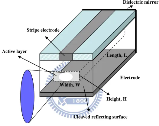
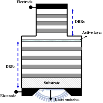
Different types of semiconductor lasers could be classified as edge-emitting and surface-emitting lasers which will be mentioned in section 1.3. The optical cavity of edge-emitting semiconductor lasers is formed by the cleaved facets perpendicular to plane of active layer structure. Therefore, the emitted photon is propagating in path normal to the epitaxial direction guided by the interfaces between active and confined layers. Schematic description of the edge-emitting lasers or the so-called Fabry-Pérot lasers is shown in Fig. 1.1-1. Because of the long active region length L, the cavity gain of edge-emitting laser is pretty high and the output power is much higher than surface-emitting laser. But the active region height H, which is equivalent to active layer thickness, is typically two orders smaller than the width W and the output beam is elliptically shaped with poor beam quality. Alternatively, the surface-emitting lasers are developed with output light direction parallel to the epitaxial direction. The laser cavity is conventionally formed by two distributed Bragg mirror (DBR) structures which are parallel to the epitaxial layer on top and bottom side of semiconductor gain chip. A simplified schematic illustration of surface-emitting lasers is shown in Fig.
1.1-2. Because there is no restriction of lateral dimensions and the cavity has circular
cross-section geometry, the output laser beam could be a single transverse mode non-diffraction limit beam. But the low optical gain due to short active length and the small current injection aperture due to the ultra-short linear-linear cavity limited the output power to just several milli-watts. Therefore, the optical pumping instead of current injection is used in external-cavity surface-emitting lasers which has been developed to obtain high power and good beam quality semiconductor laser source.
Length, L
Height, H Width, W
Dielectric mirror
Cleaved reflecting surface Elliptical laser beam
Active layer
Electrode Stripe electrode
Electrode Electrode DBRs DBRs Substrate Active layer Laser emission
The detailed evolution of surface emitting lasers will be further discussed in section 1.3.
The material system is important to the emission spectral range of semiconductor lasers which could be tuned from 400 nm in the ultraviolet by GaN-based system, to 2.3 μm by AlGaAsSb-based system. To select suitable substrate and semiconductor alloy epitaxial layers, the use of a lattice constant versus bandgap energy diagram is needed [2]. The chosen semiconductor materials in active layer should have direct bandgap matched to the objective emission photon energy. Besides, the lattice constant should be lattice-matched to the substrate and prevent the generation of large amount of defects. In using the approximation of Vegard’s law, the lattice constant and bandgap shift could be continuously tuned via the mixed ternary of quaternary alloys instead of using binary compounds [3]. The mostly mature and used material system is the compounds composed by AlAs/GaAs/InAs alloys lattice-matched to the GaAs substrate. The wavelength range of AlxGa1-xAs with mole fraction x could be varied from 780 nm to 900 nm with direct bandgap and nearly perfect lattice-matching to GaAs substrate. With the indium-doping in place of aluminum-doping, the compressive strain of the InGaAs on the GaAs substrate will make the bandgap shifted to around 1 μm. Although the more doping fraction of indium could alter the emission wavelength to be longer than 1 μm, the more serious strain effect will introduce more defects which will result in much scattering loss and lower the semiconductor laser efficiency. But this restriction could be eased by low temperature growth or by alternating growth of large and small lattice constant material to cancel the built-in energy of the MQWs which is called “strain compensation” [4]. The high refractive index difference and high thermal conductivity of the AlAs/GaAs distributed Bragg reflectors (DBRs) for GaAs-based system is also beneficial to the
development in surface-emitting lasers.
Semiconductor lasers at 1.3 and 1.55 μm are of great importance in remote sensing, laser ranging and optical communication. The InGaAsP and AlGaInAs quaternary compounds based on InP substrate and InGaNAs quaternary compound based on GaAs substrate are typically used in this spectral region. Although the InGaAsP/InP system is developed earlier than AlGaInAs/InP system, the conduction band offset of the former is smaller than the latter. This means that the carrier confinement and thermal stability under room temperature operation of InGaAsP/InP system is worse than AlGaInAs/InP system. Therefore, in this thesis we choose AlGaInAs/InP system as our MQWs material and a series of characteristics of photoluminescence, stimulated emission and saturable absorption in the surface- emitting scheme have been investigated in the following three chapters. But the DBRs lattice matched to the InP-based systems suffer from low refractive index contrast, low thermal conductivity and high complexity of growth to realize the surface-emitting laser. Alternatively, Fe-doped InP with good transparency at 1-2 μm is chosen as the substrate in our MQW sample instead of the conventionally used S-doped InP. Consequently, the transmitted AlGaInAs MQW chip is achieved and the function of DBRs could be replaced by an external mirror in the surface-emitting laser. Recently, a new GaAs-based nitride quaternary compound is applied in the semiconductor lasers in the spectral range of 1.1-1.6 μm. By introducing a few fraction of nitride to InGaAs the emission wavelength of this quaternary compound has potential shifted to longer wavelengths and the lattice-mismatching to GaAs can be reduced. However, because the nitrogen ion is smaller than the elements in the InGaAs material, the more doping concentration of nitride will result in the more defect in the alloys. It will give rise to strong scattering loss which is unfavorable to
the semiconductor lasers. So far, several InGaNAs vertical-external-cavity surface-emitting lasers have been demonstrated at wavelength range at 1.2, 1.3 and 1.55 μm. Moreover, the wafer fusion technique which allows combining different semiconductor materials with variant lattice constant is used in the AlGaInAs/GaAs OPSLs and average output power of 2.6 W is obtained at 1.57 μm. Table 1.1-1 shows the performances and material systems of the OPSLs from visible to mid-infrared spectral region to date [5-27]. Because of the absence of efficient and mature commercial pump diode laser module, the semiconductor lasers at the spectral range below 640 nm are mostly realized by frequency-doubling of the infrared semiconductor lasers [28].
1.2 Spontaneous emission of multiple-quantum-wells
In the last section we have mentioned that the multiple-quantum-well (MQW) heterostructures have potential applications in the semiconductor lasers owing to the characteristics like versatile emission wavelength, lower laser threshold and excellent performance under room temperature operation [1,29,30]. The luminescence, absorption and carrier relaxation time of MQWs are the most important optical properties which are strongly related to material systems and epitaxial structures used in MQW samples. From the experimental point of view, MQW structures are extensively investigated by means of luminescence, absorption spectrum and optical transmittance under pump-and-probe configuration. Several characteristic features including band-edge energy, peak emission wavelength, emission linewidth, integrated luminescence intensity, and carrier lifetime as functions of temperature or excitation intensity have been studied in a variety of MQW materials [31-36]. From the theoretical aspect, the inter-band transition energy can be determined by a one-dimension Schrödinger-like equation with the envelope function approximation
[25] 5W 980nm 2μm GaSb GaInSb QW [27] 2W 1.96μm 2.35μm GaSb GaInAsSb QW [26] 1.6W 980nm 2.25μm GaSb GaInAsSb QW [21] 170mW 1250nm 1549nm InP InGaAsP QW [20] 4.8W 980nm 1480nm GaAs (wafer fused) AlGaInAs QW [18] 6.6W 980nm 1300nm GaAs (wafer fused) AlGaInAs QW [17] 3W 808nm 1250nm GaAs InGaAs QD [16] 5W 808nm 1220nm GaAs GaInNAs QW [15] 4W 808nm 1180nm GaAs InGaAs QD [11] 4.35W 808nm 1032nm GaAs InGaAs QD [10] 8W 808nm 1000nm GaAs InGaAs QW [6] 1.39W 532nm 655nm GaAs AlGaInP QD [5] ---397nm 337nm Sapphire InGaN/GaN QW [23] 4.6W 980nm 1580nm GaAs (wafer fused) AlGaInAs QW [22] 77mW 980nm 1550nm InP AlGaInAs QW [24] 1W 790nm 2μm GaSb GaInSb QW [19] 0.6W 810nm 1320nm GaAs GaInNAs QW [14] 11W 808nm 1180nm GaAs GaInNAs QW [13] 7W 808nm 1170nm GaAs InGaAs QW [12] 23.8W 808nm 1040nm GaAs InGaAs QW [9] 20W 808nm 960nm GaAs InGaAs QW [8] 0.5W 660nm 850nm GaAs AlGaAs QW [7] 1.2W 532nm 665nm GaAs AlGaInP QW Ref. Pmax λpumping λlasing Substrate Gain material [25] 5W 980nm 2μm GaSb GaInSb QW [27] 2W 1.96μm 2.35μm GaSb GaInAsSb QW [26] 1.6W 980nm 2.25μm GaSb GaInAsSb QW [21] 170mW 1250nm 1549nm InP InGaAsP QW [20] 4.8W 980nm 1480nm GaAs (wafer fused) AlGaInAs QW [18] 6.6W 980nm 1300nm GaAs (wafer fused) AlGaInAs QW [17] 3W 808nm 1250nm GaAs InGaAs QD [16] 5W 808nm 1220nm GaAs GaInNAs QW [15] 4W 808nm 1180nm GaAs InGaAs QD [11] 4.35W 808nm 1032nm GaAs InGaAs QD [10] 8W 808nm 1000nm GaAs InGaAs QW [6] 1.39W 532nm 655nm GaAs AlGaInP QD [5] ---397nm 337nm Sapphire InGaN/GaN QW [23] 4.6W 980nm 1580nm GaAs (wafer fused) AlGaInAs QW [22] 77mW 980nm 1550nm InP AlGaInAs QW [24] 1W 790nm 2μm GaSb GaInSb QW [19] 0.6W 810nm 1320nm GaAs GaInNAs QW [14] 11W 808nm 1180nm GaAs GaInNAs QW [13] 7W 808nm 1170nm GaAs InGaAs QW [12] 23.8W 808nm 1040nm GaAs InGaAs QW [9] 20W 808nm 960nm GaAs InGaAs QW [8] 0.5W 660nm 850nm GaAs AlGaAs QW [7] 1.2W 532nm 665nm GaAs AlGaInP QW Ref. Pmax λpumping λlasing Substrate Gain material
Table 1.1-1 Overview of the single-chip optical-pumped semiconductor lasers performance at different wavelength region and material systems under room-temperature operation.
method as follows [37], 2 2 * 2 ( ) ( ) ( ) ( ) 2 rnl r rnl rnl rnl rl d z V z z E z m dz , (1) where the subscript n denotes subband levels of QWs and r is corresponding to electrons (conduction band) or holes (valence band), subscript l represents heavy or light holes, m*rl is the effective mass to rl value, z is the epitaxial direction, Vr(z) is the potential height at position z, φnrl(z) is the wave function of confined carrier and Enrl is the quantized energy to the nrl value. The first inter-band electron-heave hole transition energy can then be obtained as,
1h g(0) 1Vh 1Ch
E E E E . (2) Despite of the fundamental band-to-band transition of quantized energy of MQWs, the luminescence and absorption features of exciton state which is characterized by bound electron-hole pairs have been investigated with high quality epitaxial films and under ultra-low temperature operation. However, above experiments are mostly focusing on small number of QWs below fifteen periods and low-level excitation intensity.
To further understand the behaviors of distinct luminescence features of the MQW structure under high intensity photo-excitation, much effort has been devoted to optical nonlinearities. One part of these effects is focusing on the exciton state like the phase-space filling of excitons due to the Pauli exclusion principle and the dissociation of high density excitons into the electron-hole pairs [38-40]. The other sorts of the nonlinear effects are mainly ascribed to the many-body interaction of the high density electron-hole plasma (EHP). These features include the progressive filling of higher quantized states and the band-gap renormalization [41-43]. Under
high excitation intensity, the exchange effects of the electrons and holes and the screening of Coulomb interaction will result in the band-gap reduction at no matter the occupied or vacant states [44,45]. The band-gap renormalization effects of the bulk semiconductor heterostructures have been studied experimentally and theoretically as the universal behavior independent of the band structure of materials but only in relation with the Bohr radius [46,47]. In contrast, the quasi-2D confinement of the MQW structure enhances the screening and exchange effects and strengthens the phenomenon of band-gap shrinkage [48,49]. A series of investigations have put attention on the carrier density dependence of the band-gap renormalization via the means of luminescence, absorption and line-shape analysis [48,50-53] and the optical transmission measurements by the pump-and-probe experiments [43,54,55]
with high density EHP. In these investigations, the band-gap renormalization is just characterized by the slightly red-shifted band-edge below the lowest quantized state. But another typical luminescence phenomenon in several researches in use of a large number of MQWs is demonstrated in which a sharp emission band emanating below the lowest heavy-hole exciton state has been observed under high photo-excitation intensity [43,45,56,57]. This emanation mode is ascribed to be the high density EHP many-body state luminescence in which the peak intensity grows much faster with increasing excitation intensity and the linewidth are narrower than the fundamental band-to-band transition. The requirement of large number of quantum well pairs which is confirmed to be vital to the appearance of the EHP many-body state emission
[57] elucidates that the strong optical confinement and amplified spontaneous emission effect play an important role in this particular radiative recombination process. So far, these observations are all limited to operate at cryogenic temperatures below 15 K in which the exciton single-particle state and the EHP many-body state are coexisted. This hinders the employment in practical applications such as lasers and
light emitting diodes which require high stability and thermal resistivity at room temperature.
1.3 Optically-pumped semiconductor lasers
High power and good beam quality all-solid-state lasers with circularly symmetric single transverse mode are in demand in a variety of applications like nonlinear optics and the optical communications. The diode-pumped, doped- dielectrics bulk solid-state or fiber lasers are developed to be a promising light source in these fields. However, the discrete energy level of the doped ions of these lasers limits the output wavelength coverage. In contrast, the semiconductor lasers enable the potential broad spectral range from ultra-violet to mid-infrared via the bandgap engineering. The traditional edge-emitting semiconductor lasers with high output power suffer from low beam quality which is mainly due to the extraction of light perpendicular to the growth direction. Alternatively, the surface-emitting scheme is applied in the well-known vertical-cavity surface-emitting lasers (VCSELs) to realize the single transverse mode output. The VCSELs are conventionally composed by a quantum-well (QW) active region clamped by two distributed Bragg mirrors (DBRs) with current-injection pumping. To obtain the single mode output beams the current aperture need to be smaller than 10 μm because of the short and flat-flat linear cavity. As a result, the maximum output power of the VCSELs is restricted to be lower than 15 mW.
In 1993, a new type of surface-emitting semiconductor laser in which one of the DBRs fabrication is replaced by a curved external output mirror is first reported by Hadley et al [58]. The single mode pulsed 100 mW output power of this laser whish is also called the vertical-external-cavity surface-emitting laser (VECSEL) was obtained with an enlarged carrier injection aperture of 100 μm diameter in the InGaAs gain
region. In analogy to the diode-pumped solid-state lasers, the optically-pumped VECSELs, or named as optically-pumped semiconductor lasers (OPSLs), are demonstrated by Kuznetsov et al with further scaled output power greater than 0.5 W under single mode continuous-wave operation [59]. Nowadays, the OPSLs are confirmed to allow high power single mode operation in a wide spectral range via reliable semiconductor epitaxy design and growth and efficient thermal management
[60-62].
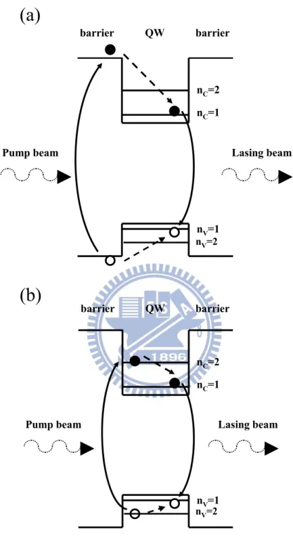
The gain chips of the OPSLs are fabricated with QW structures grown on the latticed-matched substrate via the metal-organic chemical-vapor-deposition or molecular beam epitaxy. Several epitaxial growth configurations are presented depending on the ways of thermal management [63-65] which will be further discussed in section 3.1. In this section, a typical schematic of the OPSLs is shown in
Fig. 1.3-1. The DBRs structure with 25-30 periods is first grown on the substrate with
high reflection to the pump and lasing wavelengths to serve as the front mirror. Then the active region consisted of the QWs and the barrier structure is deposited on the top of DBRs. The designation that the QWs are separated by the pump absorption barriers with half lasing wavelength interval is the resonant periodic gain (RPG) structure. Under this frame the QWs active region is located at the anti-node of the lasing standing waves to enlarge the gain exploitation [66,67]. Finally, a cap layer which is transparent to the pump and lasing wavelengths is integrated on the top of QWs to avoid the surface recombination and the oxidation. Besides, the thickness of the cap layer could be tuned to control the sub-cavity resonance due to the Fabry-Perot interference between the semiconductor-air interface and the DBRs. Then the total assembly, which is called the gain mirror, is mounted on a heat sink with substrate side to activate the heat dissipation. The gain chips are usually pumped by the
commercial laser diode array in pairs with the focusing optics with an angle of 45o to the surface normal [64,68]. But the oblique incidence makes the pump spot to be elliptical shaped. This is unfavorable to obtain single transverse mode output and will decrease the degree of mode matching. Alternatively, the end-pump schemes of OPSLs have been demonstrated in use of the modified DBR or high transmittance substrate under CW and pulsed operation [69,70].
To complete the laser cavity, an external curved mirror is added as the output coupler to ensure the high power single transverse mode output as shown in Fig. 1.3-1. The radius of curvature and the distance to the gain mirror of the external mirror are assigned to let the laser cavity mode correspond to the pump mode. Because of the short active length, the semiconductor gain mirror is inherently a low gain device in comparison to the doped-crystals in the solid-state lasers. Consequently, the reflectivity of the output mirrors in the OPSLs is typically higher than 97% under CW-operation [64,71] and the RPG structure, as mentioned above, is applied to enhance the MQW gain. As an exception, the output reflectivity could be lowered to be 92-96% or even 70% under quasi-CW and pulsed pumping [72,73]. Using the separated external mirror makes the OPSLs capable of inserting various intra-cavity components such as the nonlinear elements, spectral filters and saturable absorbers.
Although many materials as the direct emitters at visible region like the AlInGaP and GaN based systems are presented, the absence of high power and high photon energy pump source hindered the developments of the OPSLs in this field. Therefore, the second harmonics generation of the mature and efficient NIR OPSLs draws lots of interests in producing visible OPSLs. So far, a variety of the frequency doubled OPSLs with blue, green and yellow-orange light emission [74-78] are realized with fundamental emission of 920-940 nm, 960-1100 nm and1140-1250 nm, respectively.
Fig. 1.3-1 The typical gain mirror configuration of the OPSLs. Substrate .. .. DBRs MQWs Cap layer
Cooper heat sink
Coupling lens Output mirror
Gain mirror
Pump beam Laser output
To improve the wavelength conversion efficiency and enlarge the spectrum coverage, single frequency operation [79,80] and wavelength tunable OPSLs [81,82] have also been preceded. The large gain-bandwidth and gain cross-section of the semiconductor QW gain mirror are helpful in producing high-repetition rate and ultra-short passively mode-locked pulsed laser. Several passively mode-locked OPSLs with semiconductor saturable absorber mirrors (SESAMs) have demonstrated and supply giga-Hertz repetition rate and pico- to femto-seconds output pulses [83,84]. With these additional intra-cavity elements the 3- or 4- mirror SDL cavity in contrast to the traditional linear cavity as shown in Fig. 1.3-1 are applied [61] to provide intensive and focusing beam spots on these components.
1.4 Semiconductor saturable absorbers
Compact, rugged and all solid-state high peak power pulsed laser source is of great interests in many applications such as micro-processing, laser lidar, range finding and communication. To achieve the high peak power, high repetition rate and sub-nanosecond laser pulses, two intracavity modulation techniques have been extensively used. One way is using mode-locked laser in which the axial modes in the laser cavity are forced to be superimposed with a fixed phase. Consequently, the laser output will be forced to form a nearly delta function shaped pulse. The shortest duration of pulse is decided by the gain-bandwidth of the laser gain medium. The pulse-to-pulse period is equivalent to the cavity round-trip time. The other method is using the Q-switching techniques in which the population inversion density in cavity is accumulated by introducing additional loss and then release when the cavity Q value is restored to the usual large value at a suitable time interval. In general, the result of this process is the generation of a single short laser pulse with pulse duration typically several to a few tens of nanosecond long. Moreover, the practical modulation
methods of these two pulse formation techniques can be classified to active and passive modulation. The passive modulation technique is simple and no need of any electrical drivers and heat dissipation devices of the modulator. The primary method for passively Q-switched or mode-locked operation is to place a saturable absorber element inside the cavity to serve as a Q-switcher or phase modulator. The saturable absorber could be any materials with absorption band corresponding to the laser emission and has strong nonlinear saturable absorption properties. Although the organic dye solution is mostly used saturable absorber in the early stage due to its broad gain-bandwidth, the doped crystal and semiconductor saturable absorbers have taken place of it owing to the high toxicity and severely degradation under high power operation.
Mode locked laser is a promising method to produce high repetition rate and ultra-short laser pulse. But the pulse period of mode-locked laser which is equal to cavity round-trip time is too short and, as a result, the large number of pulse per second reduce the single pulse energy and could not produce pulses with high peak power even with high average output power [85,86]. Besides, the complexity and high expense and maintenance of the device configuration hinder the use in practical utilizations. Therefore, passive Q-switching of solid-state lasers which could provide high pulse energies with repetition rates in the kilo-Hz regime and nanosecond pulse width is a good alternation to produce high peak power pulsed lasers. The pulse formation process is depicted in Fig. 1.4-1. Although the pulse stabilities and periods are easy to control for the actively Q-switched lasers, the simple, low cost and monolithic fabrication and no need of high voltage electro- or acoustical-optical drivers and heat dissipation devices of passively Q-switches technique is more promising in applications requiring high peak power laser sources. Nowadays, the
bulk crystal saturable absorbers are extensively used in the passively Q-switched solid-state lasers such as Cr4+:YAG at 0.9-1.2 μm, V3+:YAG and Co2+:MgAl2O4 at 1.3 μm and Er3+:CaF and Co2+:ZnSe at 1.5 μm [87-90]. But the discrete energy level of the doped ion limited the applications of the bulk crystal saturable absorber in the more versatile spectral region. In 1996, the Nd:LSB microchip laser is firstly passively Q-switched by an antiresonant Febry-Perot SA (A-FPSA), or the so called semiconductor saturable absorber mirror (SESAM), by Braun et al. [91] with output pulse width shorter than 200 ps. In comparison to the bulk crystal saturable absorber, the advantage of SESAM is that high density of states makes the short absorption length and, therefore, the shorter cavity length even in several hundreds of microns. The Q-switching efficiency is also better because of the lower nonsaturable loss due to the shorter action length. The most important is that the absorption band of the SESAM which is decided by the bandgap of the semiconductor materials could be adapted to the gain medium at variant lasing wavelengths. Finally, there is enough design freedom of the saturable absorber parameters such as saturation fluence, modulation depth and recombination lifetime to adjust independently. Typical device structure of A-FPSAs is demonstrated in Fig. 1.4-2. In section 1.1 we have mentioned that the InP-based material system is conventionally used in the 1.3 and 1.5 μm semiconductor lasers. Because the absorption and emission wavelengths are all related to the bandgap of the semiconductors, the InGaAsP/InP and AlGaInAs/InP multiple-quantum-wells are also suitable to be fabricated as SESAMs at spectral region between 1.2-1.6 μm. But the distributed Bragg mirrors (DBRs) of InP-based semiconductor systems suffer from low refractive index contrast, low thermal conductivity or complexity in fabrication. As an alternative, semiconductor saturable absorbers (SESAs) have been developed by using an external mirror to replace the functions of DBRs. So far, numerous passively Q-switched solid-state lasers in use of
Time gain
loss
pulse formation
Output coupler Doped crystal
gain chip
A-FPSA
Dichroic beam splitter Pump laser beam
Output laser beam
Fig. 1.4-2 Typical device structure of A-FPSA used in the passively Q-switched microchip laser.
Copper heat sink
Top reflectors
High reflection at pump wavelength & partial reflection at lasing wavelength Substrate
MQW absorber layer DBRs
High reflection at lasing wavelength
SESAs with or without the DBRs have been demonstrated in the near-infrared spectral region [90-99].
Because the minimum pulse durations of the Q-switched lasers are inherently proportional to the resonator length [86,100,101], the microchip actively and passively Q-switched lasers have been developed with cavity length below 1 mm and, as a result, sub-nanosecond pulses output is obtained [86,102,103]. The ultra-short cavity length is beneficial to the single frequency operation in which the axial mode spacing is larger than the gain-banwidth. In the early stage, the Nd3+:YAG bonded to thin piece of Cr4+:YAG saturable absorber [102] and Nd, Cr-codoped YAG crystal
[104,105]are applied in the passively Q-switched microchip lasers with output pulse
durations of 337 and 290 ps around 1-μm, respectively. However, the limited doped concentration of bulk crystal SAs enlarged the cavity length and the restricted choices of the laser spectral region impede the further development as mentioned above. Therefore, high peak power and short pulse duration single frequency microchip lasers passively Q-switched by SESAM with divergent wavelength at 1 μm and at the communication region of 1.34 and 1.5 μm have beet demonstrated [90-95]. By tuning reflectivity of the top reflector, the pulse width could be varied from tens of ps to several ns range and the repetition rate from kilo- to mega-Hz with changed modulation depth and saturation intensity. Recently, the passively Q-switched microchip lasers in use of SESAMs with shortest pulse duration of 22 ps [94] and peak power up to 20 kilo-watt [106] have been reported. However, the emission wavelengths of these lasers are mainly determined by the gain mediums which are limited to the discrete energy level of doped ions.
Reference
IEEE J. Quantum Electron. QE-22, 1887-1899 (1986).
[2] U. Keller and A. C. Tropper, “Passively modelocked surface-emitting semiconductor lasers,” Phys. Reports 429, 67-120 (2006).
[3] A. R. Denton and N. W. Ashcroft, “Vegard’s law,” Phys. Rev. A 43, 3161-3164 (1991).
[4] N. J. Ekins-Daukes, K. Kawaguchi, and J. Zhang, “Strain-balanced criteria for multiple quantum well structures and its signature in X-ray rocking curves,” Cryst. Growth Des. 2, 287-292 (2002).
[5] R. Debusmann, N. Dhidah, L. Weixelbaum, U. Brauch, T. Graf, M. Weyers, and M. Kneissl, “InGaN-GaN disk laser for blue-violet emission wavelengths,” IEEE Tech. Lett. 22, 652-654 (2010).
[6] T. Schwarzbäck, R. Bek, F. Hargart, C. A. Kessler, and H. Kahle, “High-power InP quantum dot based semiconductor disk laser exceeding 1.3W,” Appl. Phys. Lett. 102, 092101 1-4 (2013).
[7] T. Schwarzbäck, M. Eichfelder, W.-M. Schulz, R. RoBbach, M. Jetter, and P. Michler, “Short wavelength red-emitting AlGaInP-VECSEL exceeds 1.2 W continuous-wave output power,” Appl. Phys. B 102, 789-794 (2011).
[8] J. E. Hastie, J.-M. Hopkins, S. Calvez, C. W. Jeon, D. Burns, R. Abram, E. Riis, A. I. Ferguson, and M. D. Dawson, “0.5-W single transverse-mode operation of an 850-nm diode-pumped surface-emitting semiconductor laser,” IEEE Photon. Tech. Lett. 15, 894-896 (2003).
[9] B. Rudin, A. Rutz, M. Hoffmann, D. J. H. C. Maas, A.-R. Bellancourt, E. Gini, T. Südmeyer, and U. Keller, “Highly efficient optically pumped vertical-emitting semiconductor laser with more than 20 W average output power in a fundamental transverse mode,” Opt. Lett. 33, 2719-2721 (2008).
[10] S. Lutgen, T. Albrecht, P. Brick, W. Reill, J. Luft, and Späth, “8-W
high-efficiency continuous-wave semiconductor disk laser at 1000 nm,” Appl. Phys. Lett. 82, 3620-3622 (2003).
[11] M. Butkus, K. G. Wilkox, J. Rautiainen, O. G. Okhotnikov, S. S. Mikhrin, I. L.
Krestnikov, A. R. Kovsh, M. Hoffmann, T. Südmeyer, U. Keller, and E. U. Rafailov, “High-power quantum-dot-based semiconductor disk laser,” Opt. Lett. 34, 1672-1674 (2009).
[12] T.-L. Wang, Y. Kaneda, J. M. Yarborough, J. Harder, J. V. Moloney, A.
optically pumped semiconductor laser at 1040 nm,” IEEE Photon. Tech. Lett. 22, 661-663 (2010).
[13] L. Fan, C. Hessenius, M. Fallahi, J. Harder, H. Li, J. V. Moloney, W. Stolz, S. W.
Koch, J. T. Murray, and R. Bedford, “Highly strained InGaAs/GaAs multiwatt vertical-external-cavity surface-emitting laser emitting around 1170 nm,” Appl. Phys. Lett. 91, 131114 1-3 (2007).
[14] V.-M. Korpijärvi, T. Leinonen, J. Puustinen, A. Härkönen, and M. D. Guina, “11
W single gain-chip dilute nitride disk laser emitting around 1180 nm,” Opt. Express 18, 25633-25641 (2010).
[15] J. Rautiainen, I. Krestnikov, J. Nikkinen and O. G. Okhotnikov, “2.5 W orange
power by frequency conversion from a dual-gain quantum-dot disk laser,” Opt. Lett. 35, 1935-1937 (2010).
[16] V.-M. Korpijärvi, M. Guina, J. Puustinen, P. Tuomisto, J. Rautiainen, A.
Härkönen, A. Tukiainen, O. Okhotnikov, and M. Pessa, “MBE grown GaInNAs-based multi-watt disk lasers,”J. Cryst. Growth 311, 1868-1871 (2009).
[17] A. R. Albrecht, T. J. Rotter, C. P. Hains, A. Stintz, J. V. Moloney, K. J. Malloy,
and G. Balakrishnan, “Multi-watt 1.25 μm quantum dot VECSEL,” Electron. Lett. 46, 856-857 (2010).
[18] A. Rantamäki, A. Sirbu, A. Mereuta, E. Kapon, and O. G. Okhotnikov, “3 W of
650 nm red emission by frequency doubling of wafer-fused semiconductor disk laser,” Opt. Express 18, 21645-21650 (2010).
[19] J.-M. Hopkins, S. A. Smith, C. W. Jeon, H. D. Sun, D. Burns, S. Calvez, M. D.
Dawson, T. Jouhti, and M. Pessa, “0.6 W CW GaInNAs vertical external-cavity surface emitting laser operating at 1.32 μm,” Electron. Lett. 40, 30-31 (2004).
[20] A. Sirbu, N. Volet, A. Mereuta, J. Lyytikäinen, J. Rautiainen, O. Okhotnikov, J.
Walczak, M. Wasiak, T. Czyszanowski, A. Caliman, Q. Zhu, V. Iakovlev, and E. Kapon, “Wafer-fused optically pumped VECSELs emitting in the 1310-nm and 1550-nm wavebands,” Adv. Opt. Technol. 2011, 209093 1-8 (2011).
[21] H. Lindberg, A. Larsson, and M. Strassner, “Single-frequency operation of a
high-power, long-wavelength semiconductor disk laser,” Opt. Lett. 30, 2260- 2262 (2005).
[22] J. P. Tourrenc, S. Bouchoule, A. Khadour, J. Decobert, A. Miard, J. C. Harmand,
with hybrid metal-metamorphic Bragg mirror,” Electron. Lett. 43, 1-2 (2007).
[23] A. Rantamäki, J. Rautiainen, J. Lyytikäinen, A. Sirbu, A. Mereuta, E. Kapon,
and O. G. Okhotnikov, “1 W at 785 nm from a frequency-doubled wafer-fused semiconductor disk laser,” Opt. Express 20, 9046-9051 (2012).
[24] A. Härkönen, M. Guina, O. Okhotnikov, K. Röβner, M. Hümmer, T. Lehnhardt,
M. Müller, A. Forchel, and M. Fischer, “1-W antimonide-based vertical external cavity surface emitting laser operating at 2-μm,” Opt. Express 14, 6479-6484 (2006).
[25] J.-M. Hopkins, N. Hempler, B. Rösener, N. Schulz, M. Rattunde, C. Manz, K.
Köhler, J. Wagner, and D. Burns, “High-power, (AlGaIn)(AsSb) semiconductor disk laser at 2.0 μm,” Opt. Lett. 33, 201-203 (2008).
[26] B. Rösener, N. Schulz, M. Rattunde, C. Manz, K. Köhler, and J. Wagner,
“High-power high-brightness operation of a 2.25-μm (AlGaIn)(AsSb)-based barrier-pumped vertical-external-cavity surface-emitting laser,” IEEE Photon. Technol. Lett. 20, 502-504 (2008).
[27] N. Schulz, M. Rattunde, C. Ritzenthaler, B. Rösener, C. Manz, K. Köhler, and J.
Wagner, “Resonant optical in-well pumping of an (AlGaIn)(AsSb)-based vertical-external-cavity surface-emitting laser emitting at 2.35 μm,” Appl. Phys. Lett. 91, 091113 1-3 (2007).
[28] S. Calvez, J. E. Hastie, M. Guina, O. G. Okhotnikov, and M. D. Dawson,
“Semiconductor disk lasers for the generation of visible and ultraviolet radiation,” Laser & Photon. Rev. 3, 407-434 (2009).
[29] K. Iga, “Surface-emitting lasers—Its birth and generation of new
optoelectronics field,” IEEE J. Sel. Top. Quantum Electron. 6, 1201-1215 (2000).
[30] S. Lutgen, T. Albrecht, P. Brick, W. Reill, and J. Luft, “8-W high-efficiency
continuous-wave semiconductor disk laser at 1000 nm,” Appl. Phys. Lett. 82, 3620-3622 (2003).
[31] D. S. Jiang, H. Jung, and K. Ploog, “Temperature dependence of
photoluminescence from GaAs single and multiple quantum-well heterostructure grown by molecular-beam epitaxy,” J. Appl. Phys. 64, 1371-1377 (1988).
[32] C. Y. Liu, S. Yuan, J. R. Dong, S. J. Chua, M. C. Y. Chan, and S. Z. Wang,
quantum well laser structure grown by metalorganic chemical vapor deposition with tertiarybutylarsine and tertiarybutyphosphine,” J. Appl. Phys. 94, 2962- 2967 (2003).
[33] X. H. Zhang, R. E. Doezema, N. Goel, S. J. Chung, M. B. Santos, N. Dai, F. H.
Zhao, and Z. S. Shi, “Photoluminescence study of InSb/AlxIn1-xSb quantum wells,” Appl. Phys. Lett. 89, 021907 1-3 (2006).
[34] E. O. Göbel, H. Jung, J. Kuhl, and K. Ploog, “Recombination enhancement due
to carrier localization in quantum well structures,” Phys. Rev. Lett. 51, 1588-1591 (1983).
[35] P. Michler, A. Hangleiter, M. Moser, M. Geiger, and F. Scholz, “Influence of
barrier height on carrier lifetime in Ga1-yInyP/(AlxGa1-x)1-yInyP single quantum wells,” Phys. Rev. B 46, 7280-7283 (1992).
[36] Y. J. Wang, S. J. Xu, Q. Li, D. G. Zhao, and H. Yang, “Band gap renormalization
and carrier localization effects in InGaN/GaN quantum-wells light emitting diodes with Si doped barriers,” Appl. Phys. Lett. 88, 041903 1-3 (2006).
[37] S. Yuan, Y. Kim, H. H. Tan, C. Jagadish, P. T. Burke, L. V. Dao, M. Gal, M. C. Y.
Chan, E. H. Li, J. Zou, D. Q. Cai, D. J. H. Cockayne, and R. M. Cohen, “Anodic-oxcide-induced interdiffusion in GaAs/AlGaAs quantum wells,” J. Appl. Phys. 83, 1305-1311 (1998).
[38] S. Schmitt-Rink, D. S. Chemla, and D. A. B. Miller, “Theory of transient
excitonic optical nonlinearities in semiconductor quantum-well structures,” Phys. Rev. B 32, 6601-6609 (1985).
[39] S. Schmitt-Rink, C. Ell, and H. Haug, “Mant-body effects in the absorption,
gain, and luminescence spectra of semiconductor quantum-well structures,” Phys. Rev. B 33, 1183-1189 (1986).
[40] S. Schmitt-Rink and C. Ell, “Excitons and electron-hole plasma in quasi-two-
dimensional systems,” J. Lumin. 30, 585-596 (1985).
[41] E. O. Göbel, R. Höger, J. Kuhi, H. J. Polland, and K. Ploog, “Homogeneous
gain saturation in GaAs/AlGaAs quantum well lasers,” Appl. Phys. Lett. 47, 781-783 (1985).
[42] Z. Y. Xu, V. G. Kreismanis, and C. L. Tang, “Stimulated emission of
GaAsAl0.6Ga0.4As multiple quantum well structures grown by metalorganic chemical vapor deposition,” Appl. Phys. Lett. 44, 136-138 (1984).
renormalization in quantum wells,” Phys. Rev. B 42, 7655-7658 (1990).
[44] C. Delalande, G. Bastard, J. Orgonasi, J. A. Brum, H. W. Liu, M. Voos, G.
Weimann, and W. Schlapp, “Mant-body effects in a modulation-doped semiconductor quantum well,” Phys. Rev. Lett. 59, 2690-2692 (1987).
[45] J. A. Levenson, I. Abram, R. Raj, G. Dolique, J. L. Oudar, and F. Alexandre,
“Optical nonlinearities in multiple quantum wells: New insight on band-gap renormalization,” Phys. Rev. B 38, 13443-13446 (1988).
[46] M. Cappizzi, S. Modesti, A. Frova, J. L. Staehli, M. Gussi, and R. A. Logan,
“Electron-hole plasma in direct-gap Ga1-xAlxAs and k-selection rule,” Phys. Rev. B 29, 2028-2035 (1984).
[47] P. Vashishta and R. K. Kalia, “Universal behavior of exchange-correlation
energy in electron-hole liquid,” Phys. Rev. B 25, 6492-6495 (1982).
[48] G. Tränkle, A. Forchel, H. Haug, C. Ell, and G. Weimann, “Dimensionality
dependence of the band-gap renormalization in two- and three-dimensional electron-hole plasmas in GaAs,” Phys. Rev. Lett. 58, 419-422 (1987).
[49] S. D. Sarma, R. Jalabert, and S.-R. E. Yang, “Band-gap renormalization in
quasi-two-dimensional systems induced by many-body electron-electron and electron-phonon interactions,” Phys. Rev. B 39, 5516-5519 (1189).
[50] H. Haug and S. Schmitt-Rink, “Basic mechanisms of the optical nonlinearities
of semiconductors near the band edge,” J. Opt. Soc. Am. B 2, 1135-1142 (1985).
[51] D. A. Kleinman and R. C. Miller, “Band-gap renormalization in semiconductor
quantum wells containing carriers,” Phys. Rev. B 32, 2266-2272 (1985).
[52] G. Tränkle, E. Lach, A. Forchel, F. Scholz, C. Ell, H. Haug, and G. Weimann,
“General relation between band-gap renormalization and carrier density in two-dimensional electron-hole plasmas,” Phys. Rev. B 36, 6712-6714 (1987).
[53] E. Lach, A. Forchel, D. A. Broido, T. L. Reinecke, G. Weimann, and W. Schlapp,
“Room-temperature emission of highly excited GaAs/Ga1-xAlxAs quantum wells,” Phys. Rev. B 42, 5395-5398 (1990).
[54] C. Webber, C. Klingshirn, D. S. Chemla, D. A. B. Miller, J. E. Cunningham, and
C. Ell, “Gain measurements and band-gap renormalization in GaAs/AlxGa1-xAs multiple-quantum-well structures,” Phys. Rev. B 38, 12748-12751 (1988).
[55] B. Deveaud, F. Clérot, K. Fujiwara, and K. Mitsunaga, “Radiative properties of
a highly excited quantum well,” Appl. Phys. Lett. 58, 1485-1487 (1991).
in two-dimensional multiple quantum wells,” Phys. Rev. B 32, 1419-1422 (1985).
[57] R. Cingolani, K. Ploog, A. Cingolani, C. Moro, and M. Ferrara, “Radiative
recombination processes of the many-body states in multiple quantum wells,” Phys. Rev. B 42, 2893-2903 (1990).
[58] M. A. Hadley, G. C. Wilson, K. Y. Lau, and J. S. Smith, “High single-
transverse-mode output from external-cavity surface-emitting laser diodes,” Appl. Phys. Lett. 63, 1607-1609 (1993).
[59] M. Kuznetsov, F. Hakimi, R. Sprague, and A. Mooradian, “Design and
characteristics of high-power (>0.5-W CW) diode-pumped vertical-external-cavity surface-emitting semiconductor lasers with circular TEM00 beams,” IEEE J. Sel. Top. Quantum Electron. 5, 561-573 (1999)
[60] M. Guina, T. Leinonen, A. Härkönen, and M. Pessa, “High-power disk lasers
based on dilute nitride heterostructures,” N. J. Phys. 11, 125019 (2009).
[61] S. Calvez, J. E. Hastie, M. Guina, O. G. Okhotnikov, and M. D. Dawson,
“Semiconductor disk lasers for the generation of visible and ultraviolet radiation,” Laser & Photon. Rev. 3, 407-434 (2009).
[62] S. Calvez, J. E. Hastie, A. J. Kemp, N. Laurand, and M. D. Dawson, “Thermal
management, structure design, and integration considerations for VECSELs,” in Semiconductor Disk Lasers: Physics and Technology, O. G. Okhotnikov, Ed. Darmstadt, Germany: Wiley-VCH Verlag GmbH, 2010, pp. 73-117.
[63] S. Lutgen, T. Albrecht, P. Brick, W. Reill, J. Luft, and W. Spath, “8-W
high-efficiency continuous-wave semiconductor disk laser at 1000 nm,” Appl. Phys. Lett. 82, 3620-3622 (2003).
[64] W. J. Alford, T. D. Raymond, and A. A. Allerman, “High power and good beam
quality at 980 nm from a vertical external-cavity surface-emitting laser,” J. Opt. Soc. Am. B 19, 663-666 (2002).
[65] R. Häring, R. Paschotta, A. Aschwanden, E. Gini, F. Morier-Genoud, and U.
Keller, “High-power passively mode-locked semiconductor laser,” IEEE J. Quantum Electron. 38, 1268-1275 (2002).
[66] M. Y. A. Raya, S. R. J. Brueck, M. Osinsky, C. F. Schaus, J. G. Mcinery, T. M.
Brennan, B. E. Hammons, “Resonant periodic gain surface-emitting semiconductor lasers,” IEEE J. Quantum Electron. QE-25, 1500-1512 (1989).
periodic-gain surface-emitting semiconductor lasers and correlated emission in a ring cavity,” Phys. Rev. A 44, 4599-4607 (1991).
[68] H. Lindberg, M. Strassner, J. Bengtsson, and A. Larsson, “High-power optically
pumped 1550-nm VECSEL with a bonded silicon heat spreader,” IEEE Photonics Technol. Lett. 16, 1233-1235 (2004).
[69] J. H. Lee, J. Y. Kim, S. M. Lee, J. R. Yoo, K. S. Kim, S. H. Cho, S. J. Lim, G. B.
Kim, S. M. Hwang, T. Kim, and Y. J. Park, “9.1-W high-efficient continuous-wave end-pumped vertical-external-cavity surface-emitting semiconductor laser,” IEEE Photonics Technol. Lett. 18, 2117-2119 (2006).
[70] K. W. Su, S. C. Huang, A. Li, S. C. Liu, Y. F. Chen, and K. F. Huang,
“High-peak-power AlGaInAs quantum-well 1.3-μm laser pumped by a diode-pumped actively Q-switched solid-state laser,” Opt. Lett. 31, 2009-2011 (2006).
[71] B. Rudin, A. Rutz, M. Hoffmann, D. J. H. C. Maas, A.-R. Bellancourt, E. Gini,
T. Südmeyer, and U. Keller, “Highly efficient optically pumped vertical-emitting semiconductor laser with more than 20 W average output power in a fundamental transverse mode,” Opt. Lett. 15, 2719-2721 (2008).
[72] A. Laurain, T.-L. Wang, M. J. Yarborough, J. Harder, J. V. Moloney, S. W. Koch,
B. Kunert, and W. Stolz, “High peak power operation of a 1-μm GaAs-based optically pumped semiconductor laser,” IEEE Photonics Technol. Lett. 24, 380-382 (2012).
[73] Y.-F. Chen, K. W. Su, W. L. Chen, K. F. Huang, and Y. F. Chen,
“High-peak-power optically pumped AlGaInAs eye-safe laser at 500-kHz repetition rate with an intracavity diamond heat spreader,” Appl. Phys. B 108, 319-323 (2012).
[74] G. B. Kim, J.-Y. Kim, J. Lee, J. Yoo, and K.-S. Kim, “End-pumped green and
blue vertical external cavity surface emitting laser device,” Appl. Phys. Lett. 89, 181106 1-3 (2006).
[75] L. Fan, T.-C. Hsu, M. Fallahi, J. T. Murray, and R. Bedford, “Tunable watt-level
blue-green vertical-external-cavity surface-emitting lasers by intracavity frequency doubling,” Appl. Phys. Lett. 88, 251117 1-3 (2006).
[76] S. Cho, G. B. Kim, J.-Y. Kim, K.-S. Kim, S.-M. Lee, J. Yoo, T. Kim, and T\Y.
Park, “Compact and efficient green VECSEL based on novel optical end-pumping scheme,” IEEE Photon. Tech. Lett. 19, 1325-1327 (2007).
[77] M. Fallahi, L. Fan, Y. Kaneda, C. Hessenius, J. Harder, H. Li, J. V. Moloney, B. Kunert, W. Stolz, S. W. Koch, J. Murray, and R. Bedford, “5-W yellow laser by intracavity frequency doubling of high-power vertical-external-cavity surface-emitting laser,” IEEE Photon. Tech. Lett. 20, 1700-1702 (2008).
[78] J. Rautiainen, A. Härkönen, V.-M. Korpijärvi, P. Tuomisto, M. Guina, and O. G.
Okhotnikov, “2.7 W tunable orange-red GaInNAs semiconductor disk laser,” Opt. Express 15, 18345-18350 (2007).
[79] M. Jacquemet, M. Domenech, G. Lucas-Leclin, P. Georges, J. Dion, M.
Strassner, I. Sagnes, and A. Garnache, “Single-frequency cw vertical external cavity surface emitting semiconductor laser at 1003 nm and 501 nm by intracavity frequency doubling,” Appl. Phys. B 86, 503-510 (2007).
[80] H. Lindberg, A. Larsson, and M. Strassner, “Single-frequency operation of a
high-power, long-wavelength semiconductor disk laser,” Opt. Lett. 30, 2260-2262 (2005).
[81] A. J. Maclean, A. J. Kemp, S. Calvez, J.-Y. Kim, T. Kim, M. D. Dawson, and D.
Burns, “Continuous tuning and efficient intracavity second-harmonic generation in a semiconductor disk laser with an intracavity diamond heatspreader,” IEEE J. Quantum Electron. 44, 216-225 (2008).
[82] L. Fan, C. Hessenius, M. Fallahi, J. Harder, H. Li, J. V. Moloney, W. Stolz, S. W.
Koch, J. T. Murray, and R. Bedford, ”Highly strained InGaAs/GaAs multiwatt vertical-external-cavity surface-emitting laser emitting around 1170 nm,” Appl. Phys. Lett. 91, 131114 1-3 (2007).
[83] R. Häring, R. Paschotta, A. Aschwanden, E. Gini, F. Morier-Genoud, and U.
Keller, “High-power passively mode-locked semiconductor lasers,” IEEE J. Quantum Electron. 38, 1268-1275 (2002).
[84] U. Keller and A. C. Tropper, “Passively modelocked surface-emitting
semiconductor lasers,” Phys. Reports 429, 67-120 (2006).
[85] J. J. Zayhowski and C. Dill III, “Diode-pumped passively Q-switched
picosecond microchip lasers,” Opt. Lett. 19, 1427-1429 (1994).
[86] J. J. Zayhowski, “Passively Q-switched Nd:YAG microchip lasers and
applications,” J. Alloys and Compounds 303, 393-400 (2000).
[87] Y. F. Chen and Y. P. Lan, “Diode-pumped passively Q-switched Nd:YAG laser
[88] A. Agnesi, A. Guandalini, G. Reali, J. K. Jabczynski, K. Kopczynski, and Z. Mierczyk, “Diode pumped Nd:YVO4 laser at 1.34 μm Q-switched and mode locked by a V3+:YAG saturable absorber,” Opt. Commun. 194, 429-433 (2001).
[89] K. V. Yumashev, I. A. Denisov, N. N. Posnov, P. V. Prokoshin, and V. P.
Mikhailov, “Nonlinear absorption properties of Co2+:MgAl2O4 crystal,” Appl. Phys. B 70, 179-184 (2000).
[90] R. Häring, R. Paschotta, R. Fluck, E. Gini, H. Melchior, and U. Keller,
“Passively Q-switched microchip laser at 1.5μm,” J. Opt. Soc. Am. B 18, 1805-1812 (1998).
[91] B. Braun, F. X. Kärtner, U. Keller, J.-P. Meyn, and G. Huber, “Passively
Q-switched 180-ps Nd:LaSc3(BO3)4 microchip laser,” Opt. Lett. 21, 405-407 (1996).
[92] B. Braun, F. X. Kärtner, G. Zhang, M. Moser, and U. Keller, “56-ps passively
Q-switched diode-pumped microchip laser,” Opt. Lett. 22, 381-383 (1997).
[93] G. J. Spühler, R. Paschotta, M. P. Kullberg, M. Graf, M. Moser, E. Mix, G.
Huber, C. Harder, and U. Keller, “A passively Q-switched Yb:YAG microchip laser,” Appl. Phys. B 72, 285-287 (2001).
[94] A. C. Butler, D. J. Spence, and D. W. Coutts, “Scaling Q-switched microchip
lasers for shortest pulses,” Appl. Phys. B 109, 81-88 (2012).
[95] R. Fluck, B. Braun, E. Gini, H. Melchior, and U. Keller, “Passively Q-switched
1.34-μm Nd:YVO4 microchip laser with semiconductor saturable-absorber mirrors,” Opt. Lett. 22, 991-993 (1997).
[96] R. Fluck, R. Häring, R. Paschotta, E. Gini, H. Melchior, and U. Keller, “Eyesafe
pulsed microchip laser using semiconductor saturable absorber mirrors,” Appl. Phys. Lett. 72, 3273-3275 (1998).
[97] A. Li, S. C. Liu, K. W. Su, Y. L. Liao, S. C. Huang, Y. F. Chen, and K. F. Huang,
“InGaAsP quantum-wells saturable absorber for diode-pumped passively Q-switched 1.3-μm lasers,” Appl. Phys. B 84, 429-431 (2006).
[98] S. C. Huang, S. C. Liu, A. Li, K. W. Su, Y. F. Chen, and K. F. Huang,
“AlGaInAs quantum-well as a saturable absorber in a diode-pumped passively Q-switched solid-state laser,” Opt. Lett. 32, 1480-1482 (2007).
[99] J. Y. Huang, H. C. Liang, K. W. Su, H. C. Lai, Y.-F. Chen, and K. F. Huang,