微污染與電漿製程對奈米電晶體元件特性影響
144
0
0
全文
(2) 微污染與電漿蝕刻對奈米電晶體元件特性影響之研究 及其改善方法之研發 Study on the Effects of Microcontamination and Plasma Process to Nano-Device Characteristics and the Development of Improvement Methods 研究生: 蕭智文. Student: Chih-Wen Hsiao. 指導教授:葉清發 博士. Advisor: Prof. Ching-Fa Yeh. 國 立 交 通 大 學 電 子 工 程 學 系 電 子 研 究 所 博 士 論 文 A Dissertation Submitted to Department of Electronics Engineering & Institute of Electronics College of Electrical Engineering & Computer Science National Chiao-Tung University for the Degree of Doctor of Philosophy in Electronics Engineering. June 2004 Hsinchu, Taiwan, Republic of China. 中華民國九十三年六月.
(3) 微污染與電漿製程對奈米電晶體元件特性影響之研究 及其改善方法之研發 研究生:蕭智文. 指導教授:葉清發 國立交通大學 電子工程學系 電子研究所. 摘 要 在超大型積體電路中,電晶體元件的尺寸必須持續微縮以降低成本及提升元件特 性,在奈米世代元件的研發上,電晶體的重要製程,包括微污染、閘極氧化層、超淺 接面及銅製程等,都是元件製作成敗的關鍵。本論文主要研究微污染防治及電漿製程 兩大主題,分別就潔淨室中微污染及電漿製程對奈米電晶體元件特性的影響,並分別 提出改良的新式製程。. 在微污染防治方面,首先我們架設一組清洗工作台,在工作台內裝置可更換的濾 網模組,分別使用新的鐵氟龍材質空氣濾網與傳統玻璃纖維空氣濾網,探討兩種濾網 對微污染的控制能力。在定性與定量分析工作台內微污染的成分及含量後,發現兩種 空氣濾網皆可有效控制包括無機離子、有機離子及金屬等微污染物,但是傳統玻璃纖 維空氣濾網由於內含黏著劑,在循環迴風下,產生了相關的有機污染物。另外,我們 製作了金氧半電容元件來評測暴露在不同濾網下,微污染對元件閘極氧化層的影響, 結果發現鐵氟龍材質空氣濾網相較於傳統玻璃纖維空氣濾網,可有效改善元件特性。. 接著,我們在工作台內使用氫氟酸氣體加速實驗來模擬潔淨室中酸性氣體的腐蝕 過程,鐵氟龍與玻璃纖維材質的空氣濾網,分別安裝在工作台內進行實驗以分析兩種 i.
(4) 空氣濾網的抗腐蝕能力,空氣採樣、晶片採樣及元件暴露實驗分別使用來探討兩種空 氣濾網在腐蝕過程中所釋放污染物的成分及含量,以及這些污染物對元件特性的影 響,結果證明鐵氟龍材質空氣濾網可有效抵抗潔淨室中酸性氣體的腐蝕,而傳統玻璃 纖維材質的空氣濾網在氫氟酸氣體的腐蝕下,釋放了包括硼及有機離子等污染物,造 成元件特性的退化。. 在電漿製程研究方面,首先我們開發製作矽化鎳的製程,分別針對鎳金屬沉積厚 度、快速熱退火溫度及製作於不同結晶的矽基板上等,尋找最佳化條件,發現在單晶 矽及非晶狀複晶矽上,200Å 厚度的鎳在 400℃到 650℃快速熱退火下形成的矽化鎳, 有較低且穩定的片電阻值。接著我們將矽化鎳製作於不同線寬的複晶矽閘極上,探討 閘極線寬對矽化鎳阻值的影響,結果顯示矽化鎳的最佳製程溫度在 400℃到 550℃之 間。然後,我們研究矽化鎳在第二次快速熱退火的熱穩定性,發現矽化鎳製作於單晶 矽與非晶狀複晶矽有較佳的熱穩定性。. 在矽化鎳製程最佳化後,我們將矽化鎳製程應用於超淺接面的製作,實驗發現接 面二極體漏電流隨著矽化鎳製程溫度增加而減少,這是由於矽化鎳完全形成所致,另 外,漏電流也會隨著矽化鎳厚度增加而增加,這是由於矽化鎳越來越接近接面二極體 的空乏區。接著,我們使用新式選擇性液相沉積法來取代傳統活性離子蝕刻法製作接 觸孔,研究二極體元件在電漿環境下元件特性退化的機制,結果發現利用選擇性液相 沉積法製作接觸孔可以抑制電漿製程對接面深度 1000Å 以下元件造成的退化。. 在本研究中,我們分別探討微污染及電漿製程對電晶體元件特性的影響,並提出 改良製程,經實驗結果證實新式鐵氟龍材質空氣濾網及選擇性液相沉積法可有效改善 元件特性,此兩項技術對應用於奈米世代元件製程,應該具有相當大的潛力。. ii.
(5) Study on the Effects of Microcontamination and Plasma Process to Nano-Device Characteristics and the Development of Improvement Methods. Student: Chih-Wen Hsiao. Advisor: Ching-Fa Yeh. Department of Electronics Engineering & Institute of Electronics, National Chiao Tung University. ABSTRACT In ULSI, the dimension of device must be scaled down to reduce the cost and improve the device performance. For the development of nanometer generation devices, the important issues, including microcontamination, gate insulator, ultra-shallow junction, copper interconnection, etc., are the key processes to successfully fabricate devices. In this thesis, the microcontamination control and the plasma process of silicide shallow junction were the main topics. The influences of microcontamination and plasma process to device performance were studied and the new improvement methods were developed. In the microcontamination control aspect, first the specially designed clean bench was set up in the cleanroom. The main filter of the clean bench was changeable and two kinds of air filter modules, including the PTFE and the glass-fiber ULPA filters, were used as the main filter, respectively. After the air sampling, wafer sampling and device exposure experiments, it was found that two kinds of air filters can effectively control the contaminants, including inorganic ions, organic ions and metals, in the cleanroom. The glass-fiber ULPA filter, however, presented some organic contaminants released from the binder of the filter in air recycling condition. Besides, the MOS capacitors were also used to investigate the effects of contaminations to gate insulator when the device were exposed under different ULPA filters. The results revealed that the PTFE ULPA filter can control the contamination and improve the device performance. Next, the hydrofluoric acid (HF) vapor was used in the clean bench to simulate the acid vapor corrosion in the cleanroom. The PTFE and glass-fiber ULPA filters were used to investigate the corrosion-resistant ability, respectively. From the air sampling, wafer iii.
(6) sampling and device exposure experiments, the PTFE ULPA filter showed better resistance to HF vapor corrosion. On the contrary, the glass-fiber ULPA filter released organic ions and boron contaminants in the HF vapor environment and resulted in the degradation of device performance. In the plasma process aspect, first the optimum process conditions of nickel silicide were developed according to the nickel film thickness, rapid thermal annealing (RTA) temperature and different crystallization substrates. The nickel silicide formed with the 200Å-thick nickel and the RTA temperature between 400℃ to 650℃ showed the low and stable sheet resistance when fabricated on the c-Si and apoly-Si substrates. The nickel silicide was also fabricated on the poly-gate with different linewidth and the results showed that the optimum process temperatures were between 400℃ to 550℃. Finally, the stability of nickel silicide processed with second RTA was studied and it was found that the nickel silicide formed on c-Si and apoly-Si substrates have the better thermal stability. The optimum processes of nickel silicide were then used to fabricate on the ultra-shallow n+/p junction. The leakage current of junction diode decreased with the increasing RTA temperature and this was due to the complete formation of nickel silicide. Besides, the leakage current of junction diode increased with the increasing nickel silicide thickness and this is because the silicide grew close to the junction depletion region. Finally, the selective liquid-phase deposition (S_LPD) method was used to replace the traditional reactive-ion etching (RIE) for the formation of contact holes. The degradation mechanism of diodes exposed under the plasma environment was investigated and the results displayed that diodes with the contact-holes formed by the S_LPD method can suppress the degradation of device with the junction depth shallower than 1000Å. In this study, the influences of microcontamination and plasma process to device performance were investigated and the new improvement methods were also proposed. The experimental results revealed that the PTFE ULPA filter and the selective liquid-phase deposition method can effectively improve the device performance and they may become the potential technologies for the fabrication of nanometer generation devices.. iv.
(7) 誌 謝 首先我要感謝我的指導教授葉清發博士,在碩士加博士六年期間,老 師不斷的督促我創新研究,並嚴格的指導實驗上的各種細節,除了研究之 外,老師並鼓勵我獨立執行各種計畫,及參與國內國外研討會,以培養上 台發表的經驗,在這六年中,雖比別人付出許多,但收穫卻更多,讓我能 非常有自信的與人談論我的研究學習過程。另外要感謝羅正忠教授在老師 不在國內的這段時間,在實驗及論文上的協助。 其次我要感謝劉建宏、李岳川、陳政忠、蘇育清、吳國豪、施鴻明、 陳添富、王超群等學長在實驗及學業上的幫助,以及我的同學林信翔、陳 啟明、許至全、林建興、李耀仁、嚴承正、蔡宗鳴及徐國鈞在我碩士班時 的幫忙。另外,我要感謝學弟詹文炘、林炫政、謝志民及李文山對於我實 驗上的幫忙及畢業論文的貢獻,感謝學弟楊瑞紋、王碩晟、薛國欽、林榮 祥及劉俊彥關於實驗上的協助。 感謝交大奈米中心(原半導體中心)技術員徐秀鑾小姐、林素珠小姐、黃 月眉小姐、陳悅婷小姐、陳聯珠小姐及彭兆光先生在使用實驗儀器上的協 助;何惟梅小姐及劉暁玲小姐在各項作業申請及工讀上的幫助;感謝國家 奈米元件實驗室趙子綾(趙國芬)小姐在 PECVD 及 Sputter 上的協助以及蔣秋 芬小姐在 PVD 方面的協助;感謝日本大金工業及 Toshio Kusumi, Hideki Aomi 兩位先生在計畫經費及實驗上的幫忙。 感謝女友 Grace 這麼多年的支持,讓我在漫長的博士研究生活中,仍然 抱持樂觀的心情過著快樂的研究生活。 最後,僅以此論文獻給我的父親蕭江龍先生及蕭黃秀貴女士,感謝他 們這些年來對我的無盡的付出與全力的支持,並感謝我的三位哥哥對我的 關心與照顧,讓我終能完成學業。 v.
(8) CONTENTS ABSTRACT (in Chinese)……………………………………………………….................... i ABSTRACT (in English)……………………………………………………………….…… iii ACKNOWLEDGEMENT.......................................................................................................... v CONTENTS……………………………………………………………................................. vi TABLE CAPTIONS…………………………………………………………………………. viii FIGURE CAPTIONS………………………………………………………………………… ix CHAPTER 1 Introduction and Thesis Organization 1.1 BACKGROUND AND MOTIVATIONS……………………………………………………... 1 1.2 THESIS ORGANIZATION………………………………………………………………… 4 CHAPTER 2 Investigation of Airborne Molecular Contamination in Cleanroom and Its Effects on Device Performance 2.1 INTRODUCTION…………………………………………………………………………. 7 2.2 EXPERIMENTS………………………………………………………………………….. 8 2.2.1 Evaluation of AMC through Air Sampling………………………………………… 8 2.2.2 Evaluation of AMC through Wafer Sampling……………………………………... 9 2.2.3 Evaluation of AMC through Electrical Characterization…………………………... 9 2.3 RESULTS AND DISCUSSION……………………………………………………………... 10 2.3.1 Air Sampling Results………………………………………………………………. 10 2.3.2 Wafer Sampling……………………………………………………………………. 11 2.3.3 Electrical Characterization Using a MOS Capacitor………………………………. 12 2.4 SUMMARY……………………………………………………………………………… 13 CHAPTER 3 Study on the Degradation of Air Filter in Cleanroom with Acid Vapor Corrosion 3.1 INTRODUCTION…………………………………………………………………………. 33 3.2 EXPERIMENTS………………………………………………………………………….. 34 3.2.1 Evaluation of AMC through Air Sampling………………………………………… 34 3.2.2 Evaluation of AMC through Wafer Sampling……………………………………... 35 3.2.3 Evaluation of AMC through Electrical Characterization…………………………... 35 3.3 RESULTS AND DISCUSSION……………………………………………………………... 36 3.3.1 Pre- and Post-corroded Fiber Structure in HF Vapor Environment……………….. 36 3.3.2 Air Sampling Results in HF Vapor Environment………………………………….. 36 3.3.3 Wafer Sampling Results in HF Vapor Environment………………………………. 37 3.3.4 Electrical Characteristics of MOS Capacitors……………………………………... 38 3.3.5 Trace Doping of MOS Capacitors…………………………………………………. 39 3.5 SUMMARY……………………………………………………………………………… 40. vi.
(9) CHAPTER 4 Development of the Nickel Silicide Process 4.1 INTRODUCTION…………………………………………………………………………. 58 4.2 EXPERIMENTS………………………………………………………………………….. 59 4.2.1 Fabrication Process of Nickel Silicide……………………………………………... 59 4.2.2 Fabrication of Nickel Silicide with Different Linewidth…………………………... 60 4.3 RESULTS AND DISCUSSION……………………………………………………………... 61 4.3.1 Nickel Silicide Formed on c-Si, poly-Si, a-Si and apoly-Si……………………….. 61 4.3.2 Surface Morphology of Ni Silicide………………………………………………… 63 4.3.3 Measurement of NiSi Sheet Resistance with Different Linewidth………………… 64 4.3.4 Thermal Stability of NiSi…………………………………………………………... 66 4.4 SUMMARY……………………………………………………………………………… 67 CHAPTER 5 Investigation of Plasma Damage-Free Selective Liquid-Phase Deposition to Contact-Hole Formation 5.1 INTRODUCTION…………………………………………………………………………. 81 5.2 LIQUID-PHASE DEPOSITION (LPD) AND ITS SELECTIVITY……………………………… 82 5.3 EXPERIMENTS………………………………………………………………………….. 84 5.3.1 Nickel Silicide Schottky Diode Using Different Contact-Hole Processes………... 84 5.3.2 Ultra-Shallow Junction n+/p Diode with Nickel Silicide………………………….. 85 5.3.3 Silicide Ultra-Shallow Junction Using Different Contact-Hole Processes………… 86 5.4 RESULTS AND DISCUSSION……………………………………………………………... 88 5.4.1 The Influences of LPD Solution and RIE Plasma Etching to Nickel Silicide……... 88 5.4.2 Nickel Silicide Schottky Diode with Different Contact-Hole Processes…………... 89 5.4.2.1 Ideality Factor of Schottky Diode………………………………………………. 89 5.4.2.2 Barrier Height of Schottky Diode………………………………………………. 90 5.4.3 I-V Characteristics of n+/p Ultra-Shallow Junction with Nickel Silicide………….. 91 5.4.3.1 Junction Depth for Different Ion Implantation Energy…………………………. 91 5.4.3.2 n+/p Junction Diodes with Different Silicide Thickness………………………... 92 5.4.3.3 n+/p Junction Diodes with Different Silicide Formation Temperature…………. 92 5.4.4 Electrical Characteristics of n+/p Diode Using Different Contact-Hole Processes... 93 5.4.4.1 Current-Voltage Characteristics………………………………………………… 93 5.4.4.2 Ideality Factor of Ultra-Shallow Junction n+/p Diode with Silicide………......... 94 5.4.4.3 Effective Energy Gap…………………………………………………………… 95 5.5 SUMMARY……………………………………………………………………………… 95 CHAPTER 6 Conclusions and Future Works 6.1 CONCLUSIONS………………………………………………………………………….. 121 6.2 SUGGESTIONS FOR FUTURE WORK……………………………………………………... 124 REFERENCES………………………………………………………………………………. 125 VITA...................................................................................................................................... 128 PUBLICATION LIST………………………………………………………………………... 129 vii.
(10) TABLE CAPTIONS CHAPTER 1 TABLE 1-1 ITRS 2003 Technology Requirements. CHAPTER 2 TABLE 2-1 Summary of Air Sampling Experimental Conditions TABLE 2-2 Summary of Wafer Sampling Experimental Conditions TABLE 2-3 Air Sampling Results of Inorganic Ions TABLE 2-4 Air Sampling Results of Metals and Boron TABLE 2-5 Air Sampling Results of Organic Compounds TABLE 2-6 Wafer Sampling Results of Metals. CHAPTER 3 TABLE 3-1 Summary of Air Sampling Experimental Conditions TABLE 3-2 Summary of Wafer Sampling Experimental Conditions TABLE 3-3 Air Sampling Results of Metals and Boron in HF Vapor Environment TABLE 3-4 Air Sampling Results of Organic Compounds in HF Vapor Environment TABLE 3-5 Wafer Sampling Results of Metals in HF Vapor Environment. CHAPTER 4 TABLE 4-1 Silicon Consumption and Film Stress for Various Silicides TABLE 4-2 Sheet Resistance of As-deposited Nickel on Different Substrates. CHAPTER 5 TABLE 5-1 Summary of Device Parameters for Different Contact-Hole Processes TABLE 5-2 Summary of Diode I-V Parameters with Different Nickel Thickness TABLE 5-3 Summary of Diode I-V Parameters with Different Silicide Formation Temperature. viii.
(11) FIGURE CAPTIONS CHAPTER 2 Fig. 2-1. Schematic diagram of specially designed clean bench. Fig. 2-2. Air sampling equipments used for evaluation of metals, inorganic and organic contaminations. Fig. 2-3. Process flow of MOS capacitor exposure experiment. Fig. 2-4. Air sampling results of inorganic ions. Fig. 2-5. Air sampling results of metals and boron. Fig. 2-6. Air sampling results of organic compounds. Fig. 2-7. The fiber structure of (a) PTFE fiber and (b) Glass fiber. Fig. 2-8. Wafer sampling results of metals. Fig. 2-9. TDS-APIMS analysis for Blank sample: (a) Time depend ion intensity plot, (b) Mass spectrum at temperature = 336℃. Fig. 2-10. TDS-APIMS analysis for CB_PTFE filter sample: (a) Time depend ion intensity plot, (b) Mass spectrum at temperature = 336℃. Fig. 2-11. TDS-APIMS analysis for CB_GF filter sample: (a) Time depend ion intensity plot, (b) Mass spectrum at temperature = 336℃. Fig. 2-12. TDS-APIMS analysis for CR sample: (a) Time depend ion intensity plot, (b) Mass spectrum at temperature = 336℃. Fig. 2-13. J-E curves of MOS capacitors: (a) PTFE filter and (b) Glass fiber filter. Fig. 2-14. Breakdown field distribution of MOS capacitors: (a) Blank samples, (b) PTFE filter, and (c) Glass fiber filter. Fig. 2-15. Cumulative probability of leakage current density under different exposure environments. Fig. 2-16. Qbd Weibull plot of MOS capacitors under different exposure environments.. CHAPTER 3 Fig. 3-1. Schematic diagram of specially designed clean bench with the HF vapor. Fig. 3-2. Air sampling equipments used for the evaluation of metals and organic contaminations. Fig. 3-3. Process flow of MOS capacitor exposure experiment used to evaluate the electrical characteristics. ix.
(12) Fig. 3-4. Process flow of MOS capacitor exposure experiment used to evaluate the surface doping concentration. Fig. 3-5. The SEM photographs of (a) PTFE-fiber and (b) Glass-fiber structures. Fig. 3-6. Air sampling results of metals and boron in HF vapor environment. Fig. 3-7. Air sampling results of organic compounds in HF vapor environment. Fig. 3-8. Wafer sampling results of metals in HF vapor environment. Fig. 3-9. TDS-APIMS analysis for Blank sample: (a) Time depend ion intensity plot, (b) Mass spectrum at temperature = 400℃. Fig. 3-10. TDS-APIMS analysis for CB_PTFE filter sample: (a) Time depend ion intensity plot, (b) Mass spectrum at temperature = 400℃. Fig. 3-11. TDS-APIMS analysis for CB_GF filter sample: (a) Time depend ion intensity plot, (b) Mass spectrum at temperature = 400℃. Fig. 3-12. TDS-APIMS analysis for CR sample: (a) Time depend ion intensity plot, (b) Mass spectrum at temperature = 400℃. Fig. 3-13. The leakage current density distribution of MOS capacitors under different exposure environments. Fig. 3-14. Weibull plots of charge-to-breakdown (Qbd) characteristics of MOS capacitors under different exposure environments. Fig. 3-15. Silicon surface doping concentration of MOS capacitors under different exposure environments.. CHAPTER 4 Fig. 4-1. Fabrication process flow of the of nickel silicide. Fig. 4-2. Fabrication process flow of poly-line with nickel silicide. Fig. 4-3. Sheet resistance of NiSi formed on c-Si. Fig. 4-4. Sheet resistance of NiSi formed on poly-Si. Fig. 4-5. Sheet resistance of NiSi formed on a-Si. Fig. 4-6. Sheet resistance of NiSi formed on apoly-Si. Fig. 4-7. Top view SEM micrographs of Ni-silicide on poly-Si at different RTA temperature. Fig. 4-8. Top view SEM micrographs of Ni-silicide on a-Si at different RTA temperature. Fig. 4-9. Top view SEM micrographs of Ni-silicide on apoly-Si at different RTA temperature. Fig. 4-10. Bridge resistor structure. Fig. 4-11. Sheet resistance of different linewidth NiSi formed on poly-Si. x.
(13) Fig. 4-12. Sheet resistance of different linewidth NiSi formed on a-Si. Fig. 4-13. Sheet resistance of different linewidth NiSi formed on apoly-Si. Fig. 4-14. Sheet resistance of NiSi formed with 200Å thick Ni. Fig. 4-15. Sheet resistance of NiSi on C-Si for RTA-2 annealing. Fig. 4-16. Sheet resistance of NiSi on poly-Si for RTA-2 annealing. Fig. 4-17. Sheet resistance of NiSi on a-Si for RTA-2 annealing. Fig. 4-18. Sheet resistance of NiSi on apoly-Si for RTA-2 annealing.. CHAPTER 5 Fig. 5-1. The schematic diagram of LPD apparatus. Fig. 5-2. The process flow of preparing S_LPD solution. Fig. 5-3. The process window of S_LPD. Fig. 5-4. SEM photographs of (a) No deposition, (b) Selective deposition and (c) Blanket deposition. Fig. 5-5. Process flow of nickel silicide schottky diodes with contact-hole prepared by (a) S_LPD and (b) LPD_RIE, TEOS_RIE, and TEOS_BOE. Fig. 5-6. Process flow of ultra-shallow junction n+/p diodes with contact-hole prepared by (a) S_LPD and (b) LPD_RIE, TEOS_RIE, and TEOS_BOE. Fig. 5-7. The sheet resistance variation of nickel silicide after the treatment of (a) Chemical solutions and (b) RIE plasma. Fig. 5-8. The current-voltage characteristics of schottky diodes with different contact-hole processes. Fig. 5-9. The ideality factor variation of schottky diode with (a) Different contact-hole processes and (b) Different diode area. Fig. 5-10. (a) Richardson plot and (b) Barrier height of different contact-hole processes. Fig. 5-11. SIMS depth profiles with different ion implantation energy. Fig. 5-12. I-V characteristics of n+/p ultra-shallow junction diodes with different nickel thickness. Fig. 5-13. (a)Reverse leakage current and (b) Forward current distribution of n+/p ultra-shallow junction with different nickel thickness. Fig. 5-14. I-V characteristics of n+/p ultra-shallow junction diodes with different silicide formation temperature. Fig. 5-15. (a) Reverse leakage current and (b) Forward current distribution of n+/p ultra-shallow junction with different silicide formation temperature. xi.
(14) Fig. 5-16. I-V characteristics of silicide ultra-shallow junction with different contact-hole processes. Fig. 5-17. (a) Reverse and (b) Forward current distribution of silicide ultra-shallow junction with different contact-hole processes. Fig. 5-18. The leakage current density of different peripheral length to area ratio. Fig. 5-19. The ideality factor distribution of n+/p diodes for different contact-hole processes. Fig. 5-20. The (a) Reverse and (b)Forward current-voltage characteristics of different temperature for S_LPD sample. Fig. 5-21. The (a) Reverse and (b)Forward current-voltage characteristics of different temperature for LPD_RIE sample. Fig. 5-22. The (a) Reverse and (b)Forward current-voltage characteristics of different temperature for TEOS_RIE sample. Fig. 5-23. The (a) Reverse and (b)Forward current-voltage characteristics of different temperature for TEOS_BOE sample. Fig. 5-24. The Arrhenius plot of diodes for different contact-hole processes.. xii.
(15) CHAPTER 1 Introduction and Thesis Organization. 1.1 BACKGROUND AND MOTIVATIONS In ULSI, the dimension of device must be scaled down to reduce the manufacturing cost and improve the circuit performance. As the device size is scaled down to nanometer generation, the development of advanced processes including wafer environment contamination control, gate insulator, ultra-shallow junction, interconnection, etc., become more and more crucial to fabricate nano-dimension devices. The recently developed technologies, including high-K gate insulator, metal gate, silicide, Cu damascene process, low K dielectric, etc., have been the inevitable trend for future device manufacturing. Table 1-1 shows the technology requirements predicted by ITRS 2003. Among these key processes, wafer environment contamination control and plasma process have been considered to be well-developed technologies and pay less attention on them. The impact of AMC and plasma process on device performance can only be expected to become more deleterious as device dimensions decrease to nanometer generation. There is definitive consensus that as device geometries approach 90 nm and beyond, wafer isolation will prove to be an enabling technology. The percentage of process steps affected by non-particulate or molecular contamination is expected to increase. The use of copper and other novel materials in the process introduces other potential contaminants. Because of these trends, wafer isolation technology, integrated tool mini-environments and closed carriers (e.g., Front Opening Unified Pods (FOUPs)) are needed [1]. The wafer environment contamination control (WECC) technology requirements indicate target levels of -1-.
(16) ambient acids, bases, condensables, dopants, and metals for specific process steps. Outgassing from materials of construction in the cleanroom, wafer processing equipment, and wafer environmental enclosures as well as fugitive emissions from chemicals used in wafer processing are the two main sources of Airborne Molecular Contamination (AMC). Oxygen and water vapor as well as low concentration atmospheric contaminants (e.g., CO) can also be considered as part of the AMC burden [2]. Acid vapors in the air come from the cleaning or etching process have been often seen during the wafer processing. These acid vapors may corrode the construction of cleanroom, releasing the boron, organic compounds and amines [3]. For example, the HF vapor makes the glass-fiber in HEPA filter degraded and the boron and organic compounds contained in HEPA filter will thus be released to the wafer surface [4]. Theses contamination will impact the device performance or DUV photoresists [5]. The impact of AMC on wafer processing can only be expected to become more deleterious as device dimensions decrease. For the MOSFET device, the fabrication of source/drain (S/D) junction is an important process. With the scaling down of devices, the S/D junction depth must reduce to mitigate the punch-through phenomenon or other short-channel effects. The improvement of devices performance by the shrinking of devices size resulted in the increase of sheet resistance (RS) and contact resistance (RC). The increase of RS and RC will increase the resistance of junction area, causing the RC time delay. Since the reduction of junction area, junction depth and contact-hole size in an unsilicided device results in a high resistance junction area, it will degrade the transistor current drivability and increase the RC time delay, making the device fail to work properly. In order to reduce the parasitic resistance of the MOSFET device, the low resistivity silicide form on the junction region is required. Besides, the use of self-aligned silicide (salicide) process can selectively form silicide on the gate and the S/D region without. -2-.
(17) additional mask, which simultaneously reduced the gate and junction resistance. It is well known that the resistivity of commonly used titanium silicide (TiSi2) increases as the gate linewidth reduces to submicron dimension. For the wide lines, the TiSi2 is mainly the low resistivity C54 phase (10~15µΩ-cm), while for the narrow lines, the phase transformation process is limited and the high resistivity C49 phase (60~80µΩ-cm) is dominant. Besides, the high temperature (800~950℃) silicidation process is needed to make the C54 phase [6], [7]. However, as the thickness of Ti decreases, TiSi2 agglomeration has been observed. This results in the high sheet resistance when thin TiSi2 layers are used for the shallow junctions. For 0.18µm process or below, cobalt silicide (CoSi2) is more preferred due to its lower linewidth dependence of sheet resistance. CoSi2, however, consumes more silicon volume than TiSi2 and it will limit the scaling of junction depth. Compared to CoSi2, nickel silicide (NiSi) has the advantages: (1) less silicon consumption for the same sheet resistance, (2) low contact resistivity, (3) low process temperature and wide process window (400-600℃), (4) low stress, and (4) no creep-up phenomenon. According to the above mentioned, NiSi is a promising candidate silicide for next generation devices. Reactive ion etching (RIE) is the most frequently used technology for contact-hole formation [8]. It is important to reduce the RIE damages on the surface of junction especially for ultra-shallow junction. It has been reported that the RIE process can induce some unwanted effects including radiation damage, surface amorphized layer and contaminated layer [8]-[11]. The radiation damage results from the energetic ions accelerated by DC bias. The surface amorphized layer comes from the ion bombardment damage to junction surface. And the contaminated layer is due to the fluorocarbon-containing based etching chemistries. This damage layer is around hundred of angstroms deep from the surface. Some technologies [8], [9] are used to eliminate this surface damage layer including high temperature annealing, surface etching, etc. But these methods may not suitable for silicide process and ultra-shallow -3-.
(18) junction when manufacturing ULSI.. 1.2 THESIS ORGANIZATION In this thesis, the wafer environment contamination control and the plasma process of silicide shallow junction were the main topics. The influences of AMC and plasma process to device performance were studied and the new improvement methods were developed. In chapter 2, a clean bench with different filter modules such as the NEUROFINE PTFE filter, the glass-fiber ULPA filter, and a combination of chemical filters with both of these was set up in the cleanroom. All elements in the air or on the wafer were analyzed through air sampling and wafer sampling inside the bench, to determine clearly the ability of each filter module to suppress AMC. The practical effects of AMC on device performance were also investigated by actually exposing a wafer to air in an especially controlled clean bench before gate oxidation. In chapter 3, the performance of two ULPA filter modules - the PTFE and the glass-fiber was investigated. PTFE fiber is considered to be resistant to acid vapor corrosion and it is a good material from which to fabricate ULPA filters. The source of AMC and the effects of AMC on devices exposed in the clean bench in a HF vapor environment were examined to elucidate the impact of filter material. The results indicated that the PTFE ULPA filter can provide a better cleanroom environment than a commercial glass fiber ULPA filter. In chapter 4, the optimum process condition of NiSi on different silicon substrates and the relation between sheet resistance and linewidth were investigated. In addition, the thermal stability of NiSi processed with second rapid thermal annealing (RTA) was also studied. In chapter 5, a new selective liquid-phase deposition (S_LPD) process was proposed to overcome the RIE damage problems. S_LPD process is the selective deposition technology -4-.
(19) which deposits silicon dioxide on silicide surface against photoresist. This technology was conduct under non-plasma environment and hence it will not induce the surface damaged and contaminated layer. The experimental results indicate that the new S_LPD process indeed has the superior of suppressing plasma damage on devices. Therefore, the new S_LPD process may become the candidate of non-plasma process for future advanced device manufacturing. Finally, conclusions and recommendations for further research were summarized in Chapter 6.. -5-.
(20) TABLE 1-1 ITRS 2003 Technology Requirements Year of Production. 2003. 2004. 2006. 2007. 2008. 2009. 107 65 45. hp90 90 53 37. 80 45 32. 70 40 28. hp65 65 35 25. 57 32 22. 50 28 20. Equivalent physical oxide thickness for MPU/ASIC Tox (nm). 1.3. 1.2. 1.1. 1.0. 0.9. 0.8. 0.8. Drain extension Xj (nm). 24.8. 20.4. 17.6. 15.4. 13.8. 8.8. 8.0. Maximum drain extension sheet resistance (PMOS)(Ω /sq). 545. 663. 767. 833. 884. 1739. 1800. Maximum drain extension sheet resistance (NMOS) (Ω/sq). 255. 310. 358. 389. 412. 811. 840. 35.2 17.6 21 7.5. 30.8 15.4 19 8.6. 27.5 13.8 17 9.6. NA 13.2 16 10.0. NA 12 14 11.1. 1.44E-07. 1.20E-07. 1.05E-07. 0.87E-07. 0.72E-07. Technology Node MPU/ASIC ½ Pitch (nm). MPU Printed Gate Length (nm) MPU Physical Gate Length (nm). Contact Xj (nm) 49.5 40.7 Maximum silicon consumption (nm) 24.8 20.4 Silicide thickness (nm) 25 20 Contact silicide sheet Rs (Ω/sq) 6.5 7.9 1.62E-07 Contact maximum resistivity (Ω-cm2) 1.93E-07 Airborne Molecular Contaminants in gas phase (pptM)) Lithography—bases (as amine, amide, and NH3) Gate—metals (as Cu, E=2×10⁻⁵) Gate—organics (as molecular weight to 250, E=1×10⁻³) Dopants. 2005. 750. 750. 750. <750. <750. <750. <750. 0.15. 0.1. 0.1. 0.07. <0.07. <0.07. <0.07. 80. 70. 60. 60. 50. 50. 50. <10. <10. <10. <10. <10. <10. <10. Airborne Molecular Contaminants, Surface Deposition Limits (for Si Witness Wafer, 24-hour Exposure to Closed FOUP, Pod, Mini-environment or Air) SMC organics on wafers, ASTM 1982–99, ng/cm2 Front-end processes, bare Si, total dopants added to 24-hour witness wafer, atoms/cm2 Front-end processes, bare Si, total metals added to witness wafer, atoms/cm2. 4. 2. 2. 2. 2. 2. 2. <2E12. <2E12. <2E12. 1E12. 1E12. 1E12. 1E12. <2E10. <2E10. <2E10. <2E10. <2E10. <2E10. <2E10. SMC-Surface Molecular Condensable. -6-.
(21) CHAPTER 2 Investigation of Airborne Molecular Contamination in Cleanroom and Its Effects on Device Performance. 2.1 INTRODUCTION The cleanness of a cleanroom environment must be tightly controlled to achieve high-yield and high-performance ULSI manufacturing [12]-[15]. Recently, new developments of material and process have helped to shrink device geometry. The advanced contamination control of cleanrooms has also been indispensable in this regard [16]. So far, only particle contamination has been intensively studied [17], and recently developed filters, such as HEPA and ULPA, can already sufficiently suppress particles [18]. However, the controllability of airborne molecular contamination (AMC) by present cleanroom technologies has not yet been validated because AMC is a kind of atom or molecular-level gas-phase contamination like organic and inorganic ones. As the minimum feature size of devices is continuously scaled down to far below 0.1µm, AMC will gradually become crucial in ULSI manufacturing. In the near future, especially in the nanodevice era, contamination by organic compounds, inorganic ions, and trace doping impurities [19] in cleanroom air may also dominate the characteristics, reliability, and even yield of devices. Technologies for eliminating both particles and AMC from manufacturing environment must be considered to completely solve this problem. To date, several investigations of AMC, and its effects on device performance, have been conducted. Most, however, have only paid attention to the experiments based on intentional contamination on devices [14], [20], [21]. Few studies have considered AMC absorbed from cleanroom air and its practical effects on the characteristics of devices. -7-.
(22) In this work, a clean bench was specially equipped with different filter modules such as the NEUROFINE PTFE filter, the glass-fiber ULPA filter, and a combination of chemical filters with both of these. All elements in the air or on the wafer were analyzed through air sampling and wafer sampling inside the bench, to determine clearly the ability of each filter module to suppress AMC. The practical effects of AMC on device performance were also investigated by actually exposing a wafer to air in an especially controlled clean bench before gate oxidation.. 2.2 EXPERIMENTS A specially controlled and fabricated clean bench (CB) was set up in the cleanroom (CR) of class 10k in a laboratory. Figure 2-1 schematically depicts the CB. Cleanroom air, from the air inlet of the CB, was initially filtered with the filter module that included inorganic and organic ion chemical filters, before flowing through the main filter, which was designed to be changeable. The chemical filter is mainly composed of active carbon, and it can absorb ions. Two kinds of main filter were used, the NEUROFINE PTFE filter (PTFE) and the glass-fiber ULPA filter (GF). The air flow rate and turnover rate inside the CB were set to 0.4 m/s and 5 %, respectively. Before sampling, the CB was first operated for more than one week to stabilize environmental conditions. 2.2.1 Evaluation of AMC through Air Sampling Figure 2-2 presents the air sampling tools, Impinger and TENAX, which were equipped with a flow meter and a pump. The flow rate and sampling time of Impinger were 2 L/min and 24-72 hrs while those of TENAX were 100 mL/min and 5 hrs. Impingers collected mainly both inorganic and metallic contamination elements. The former were analyzed by the ion chromatography (IC), while the latter were analyzed using an inductively coupled plasma mass spectrometer (ICP-MS). Organic substances were collected by a TENAX (a kind of -8-.
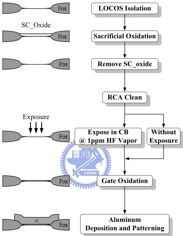
(23) absorbent) tube, and quantitatively analyzed by gas chromatograph mass spectrometer (GC-MS). The air in the CR was also analyzed for comparison. Table 2-1 summarizes the air sampling experimental conditions. 2.2.2 Evaluation of AMC through Wafer Sampling The AMC absorbed on the surfaces of actual 6” P-type (100) Si wafers was analyzed for each filter module. After standard RCA cleaning, wafers were divided into two parts, and exposed to the air in the CR and the CB for 24-72 hrs. The metal contamination on these wafer surfaces was analyzed using total reflection X-ray fluorescence (TRXRF), while the organic contamination was analyzed by thermal desorption system–atmospheric pressure ionized mass spectrum (TDS-APIMS). For comparison, the contamination of a wafer not exposed to any environment was evaluated as a control. Table 2-2 is the summary of wafer sampling experimental conditions. 2.2.3 Evaluation of AMC through Electrical Characterization Metal oxide semiconductor (MOS) capacitors, with thermal oxide as the insulator, were prepared to study the effects of AMC on practical device characteristics. Figure 2-3 shows the process flow diagram for preparing a MOS capacitor. The active region was first defined on a 6” P-type (100) Si wafer by local oxidation of the silicon (LOCOS) process, and then a 40 nm-thick sacrificial oxide layer was formed by thermal oxidation. This sacrificial oxide was subsequently removed, and the wafers were further cleaned by RCA cleaning before exposure. After exposure in the CR or the CB for 4 hrs, a 5 nm-thick gate oxide layer was grown on each wafer by thermal oxidation, and finally an aluminum gate electrode was deposited and patterned. Unexposed blank samples were also prepared using the same procedure. Finally, for all samples, the electrical properties such as leakage current density vs. electrical field (J-E), breakdown field (Ebd), and charge to breakdown (Qbd) were measured through the MOS -9-.
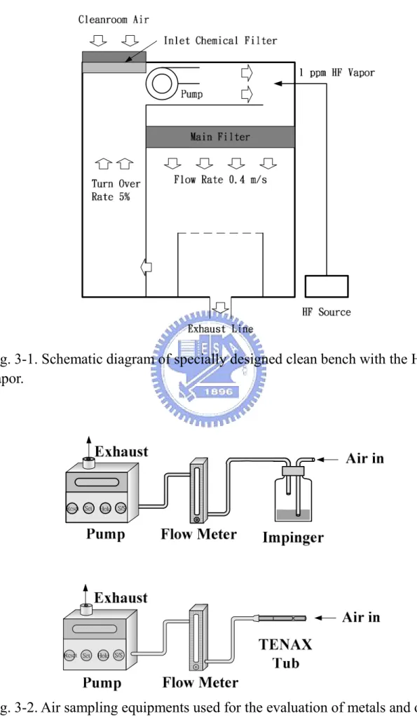
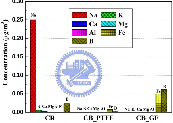
(24) capacitor (200 µm × 200 µm) using the HP4156 semiconductor parameter analyzer.. 2.3 RESULTS AND DISCUSSION 2.3.1 Air Sampling Results First, the constituents of the air in the CR and the CB, equipped with only inlet chemical filters but no main filter, were evaluated. Figure 2-4 shows the IC results for inorganic ion concentrations of the air in the CR and the CB. The concentrations of inorganic ions such as NH4+, Cl-, NO2-, NO3-, and SO42- were found to be high in the CR. In contrast, the inorganic ions concentrations in the CB were obviously low, implying that the CB without a main filter but with chemical filters can still remove the inorganic contaminations, especially NH4+ ions. All the analysis data of inorganic ions were list in Table 2-3. Next, the PTFE filter was installed as main filter in the CB and the same sampling procedure was implemented. The result was very similar to that obtained only with the chemical filters. These experimental results suggest that chemical filters efficiently reduced inorganic ion contaminations [22]. Figure 2-5 presents the ICP-MS results of metals and boron concentrations in the air from the CR and the CB. And Table 2-4 shows the ICP-MS analysis data .The concentrations of K, Mg, and Al elements were all below the detection limit in the air from the CR and from the CB without main filter, but the concentrations of Na, Ca, and especially B were detected. However, for the CB with either PTFE or GF as the main filter, both the metal and the boron contamination levels were under the detection limit. In fact, the chemical filters do not remove boron or metal contamination. Boron and metal contamination can be reasonably considered to exist in complexes with particles, and are thus more efficiently eliminated when the main filter is used than when it is not. The concentrations of organic compounds in the air from the CR and the CB were also. - 10 -.
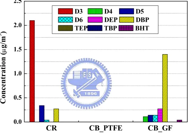
(25) compared in Table 2-5. As shown in Fig. 2-6, the organic compounds can be mainly divided into Si-based and oil-based ones. The former included D3 (C6H18O3Si3), D4 (C6H24O4Si4), D5 (C10H30O5Si5), and D6 (C12H36O6Si6), while the latter included DEP (C12H14O4), DBP (C16H22O4), TEP (C8H15O4P), TBP (C12H27O4P), and BHT (C15H24O). The CR air included high quantities of both kinds of organic compounds, but they can be mostly removed when only chemical filters were used. Of course, the concentrations can be further reduced using a combination of chemical filters and the PTFE or the GF main filter. Notably, however, a high concentration of D6 remains in the CB with a GF filter, perhaps because this compound is present in the binder of the glass-fiber ULPA filter, or in some of the materials used to manufacture the filter. Figure 2-7 shows the essential difference between the fiber structure of the PTFE filter and that of the GF filter. The glass-fiber used as an intermediate in the GF filter is usually shorter than the PTFE-fiber used in the PTFE filter. Hence, it must be mixed with a binder to reduce the gaps and ensure that the filter can isolate particles. However the binder, which consists mainly of acrylic, is an organic contamination source of D6. Consequently, the total concentration of organic compounds present when a GF filter is used exceeds that obtained when a PTFE filter is used. The high organic contamination may degrade the characteristics of devices. 2.3.2 Wafer Sampling Metal contamination on wafers exposed in the CR or the CB was quantified by TRXRF analysis. As shown in Fig. 2-8, the densities of metal on different wafers are compared and the detail data were shown in Table 2-6. The “BLANK” sample refers to a wafer treated only by RCA cleaning and unexposed to air before analysis. On each wafer, five points were analyzed and the averages of the results at these points were compared. The metal densities on the BLANK and the CB samples were all below the order of 1011 atoms/cm2, but they were. - 11 -.
(26) distributed from 1011 to 1013 atoms/cm2 on the CR samples, again showing that the CB sample when a main filter, PTFE or GF, is used indeed has the same concentration of metal as the BLANK sample. The results of TRXRF are rather consistent with those obtained by ICP-MS analysis, shown in Fig. 2-5. In PTFE or GF filter environments, the metal concentrations are the same, so the PTFE filter can replace the commercial glass fiber ULPA filter to meet the requirements of an advanced cleanroom. Next, the intensity of organic contaminant species on the wafer surfaces, exposed or unexposed to air, were evaluated using TDS-APIMS. Figure 2-9 to Fig. 2-12 compares results for different samples. The concentrations of each specifies of organic contamination of the CR sample greatly exceeded that of the CB sample, revealing that the wafer surface exposed in the CR does absorb much organic contamination. Here, mass numbers m/z = 16, 45, 73, 99, 149 were chosen. Contamination peaks at m/z = 16, 45, 149 often come from the outgassing of oil based plasticizers, which are widely used in plastic products of the cleanroom, such as DEP and DBP. Peaks at m/z = 73, 99 are often associated with the absorption of Si-based siloxane, such as D5 and D6. For all the CB samples, the intensity of m/z = 99 for a GF filter exceeds that for a PTFE filter. The result is quite consistent with the air sampling results presented in Fig. 2-6. Overall, a combination of chemical and PTFE filters in a CB can provide an excellent environment with rather low concentrations of organic compounds for manufacturing advanced ULSI devices. 2.3.3 Electrical Characterization Using a MOS Capacitor Figure 2-13 compares J-E curves of the samples exposed in the CB and the unexposed sample. Figure 2-13(a) reveals that the sample exposed under a PTFE filter has a similar leakage current density and breakdown field to the unexposed sample. The environment in the CB with the PTFE filter is excellent so the sample exposed even for 24 hrs - 12 -.
(27) shows little degradation. On the contrary, as shown in Fig. 2-13(b), the sample under a GF filter reveals a large leakage current density and exhibits much earlier breakdown than the unexposed sample. Fig. 2-14 compares the distributions of the breakdown electrical fields for these three kinds of samples. The breakdown fields were 13-14 MV/cm for the unexposed samples, while they were spread over a wide range, but still mainly 12-13 MV/cm, for the PTFE samples. However, for the GF samples, the distribution was spread even more widely, and shifted to a low electrical field. The degradation of the leakage current and the breakdown field can be attributed to AMC, which, when adhering to the wafer surface may induce defects within the gate oxide. While the MOS device is operating, the intermediate oxide defects will result in electron tunneling, rapidly inducing more defects until defect clusters form a conductive path between the substrate and the gate. Figure 2-15 plots the cumulative probabilities of leakage current densities for these three kinds of samples. In each case, the leakage current density was measured at 4 MV/cm. The PTFE samples perform similarly to the unexposed samples because the CB with the PTFE filter can create an excellent environment. In contrast, the GF samples still show a higher and less uniform leakage current density distribution than the PTFE and the unexposed samples. Figure 2-16 displays a Weibull plot of charge to breakdown (Qbd) for different samples. The PTFE samples showed slight degradation in Qbd compared to the unexposed samples, but the GF samples exhibited obvious degradation with low and non-uniform distribution. The above electrical results indicate that the PTFE filter is much better than the GF filter at creating an advanced clean environment for manufacturing devices.. 2.4 SUMMARY AMC in air and on the surfaces of wafers was quantitatively analyzed. Air sampling results reveal that a CB with chemical filters can only effectively remove inorganic ions, - 13 -.
(28) while one further equipped with a PTFE main filter can eliminate not only organic contaminations but also boron and metal. A CB with a GF filter still has a high concentration of D6. Wafer sampling results also demonstrate that each filter can, indeed, reduce the metal concentration to a level that corresponds to no exposure to air. Wafers exposed under a PTFE filter have less organic contaminations than those in the CR, but a GF filter shows high contamination of silicon-based organic D6, because of the binder used in the GF filter. In summary, the results obtained by air and wafer sampling are highly consistent. The effects of AMC on device performance were also investigated using a MOS capacitor. The samples exposed in the CB under the PTFE filter have nearly the same leakage current density and breakdown field distribution as the unexposed sample, implying that the exposed wafers have few defects and exhibit slight degradation of film quality. However, the samples in the CB under a GF filter suffer an obviously degraded breakdown field, leakage current density, and Qbd because of high concentrations of organic compounds. All these results reveal that AMC will become an important issue in future nanodevice fabrication. An AMC-free manufacturing environment must be seriously considered when manufacturing nanodevices. Advanced ULPA filters, like the NEUROFINE PTFE filter combined with chemical filters, are excellent candidates for creating advanced manufacturing environments.. - 14 -.
(29) TABLE 2-1 Summary of Air Sampling Experimental Conditions Contamination Type Organic Compounds. Sampling Equipments TENAX Tube. Flow Rate. Analysis Method. 100 mL/min.. Sampling Time 5 hrs. Inorganic Ions. Impinger. 2 L/min.. 24 hrs. IC (Ion Chromatography). Metals & Boron. Impinger. 2 L/min.. 72 hrs. ICP-MS (Inductively Coupled Plasma Mass Spectrometer). GC/MS (Gas Chromatograph Mass Spectrometer). Bench Condition Filter module: 1. PTFE ULPA filter + Chemical filter 2. Glass-Fiber ULPA filter + Chemical filter Air flow rate: 0.4 m/s Turnover rate: 5% Temperature: 23 ℃. TABLE 2-2 Summary of Wafer Sampling Experimental Conditions Contamination Type Organic Compounds. Exposing Location. Exposing Time 24 hrs. Analysis Method. Elements. TDS-APIMS (Thermal Desorption System – Atmospheric Pressure Ionized Mass Spectrum). D3, D4, D5, D6, DEP, DBP, TEP, TBP, BHT. 72 hrs. TRXRF (Total Reflection X-Ray Fluorescence). Na, K, Ca, Mg, Fe, Ti, V, Cr, Mn, Co, Ni, Cu, Zn. CR and Metals. CB. Bench Condition Filter module: 1. PTFE ULPA filter + Chemical filter 2. Glass-Fiber ULPA filter + Chemical filter Air flow rate: 0.4 m/s Turnover rate: 5% Temperature: 23 ℃. - 15 -.
(30) TABLE 2-3 Air Sampling Results of Inorganic Ions Inorganic Ion (µg/m3). CR. Inlet Filter Main Filter. Detection Limit. Detection Limit. CB. -. NH4+ ClNO2NO3SO42-. 7.4 0.13 1.3 0.68 0.2. Chemical Filter -. 0.07 0.02 0.01 0.05 0.04. 0.33 0.038 0.99 0.05 < 0.03. 0.07 0.02 0.01 0.05 0.03. TABLE 2-4 Air Sampling Results of Metals and Boron Metals & Boron (µg/m3). CR. Inlet Filter Main Filter. Na K Ca Mg Al Fe B. Detection Limit. 0.006. 0.002. CB. Detection Limit. Chemical Filter 0.006. 0.001. CB_PTFE. Detection Limit. Chemical Filter PTFE Filter <0.008. 0.008. CB_GF. Detection Limit. Chemical Filter Glass-Fiber Filter <0.002. 0.002. <0.01. 0.01. <0.005. 0.005. <0.006. 0.006. <0.004. 0.004. 0.003. 0.002. 0.002. 0.001. <0.003. 0.003. <0.004. 0.004. <0.002. 0.002. <0.001. 0.001. <0.003. 0.003. <0.004. 0.004. <0.002. 0.002. <0.001. 0.001. <0.003. 0.003. <0.004. 0.004. <0.002. 0.002. 0.002. 0.001. <0.003. 0.003. <0.004. 0.004. 0.054. 0.0003. 0.063. 0.0002. <0.0006. 0.0006. <0.0007. 0.0007. - 16 -.
(31) TABLE 2-5 Air Sampling Results of Organic Compounds Organic Compounds CR (µg/m3) Inlet Filter Main Filter. Detection Limit. CB. -. D3:C6H18O3Si3 D4:C8H24O4Si4 D5:C10H30O5Si5 D6:C12H36O6Si6 DEP:C12H14O4 DBP:C16H22O4 TEP:C6H15O4P TBP:C12H27O4P BHT:C15H24O. Detection Limit. CB_PTFE. Detection Limit. Chemical Filter -. Chemical Filter PTFE Filter. CB_GF. Detection Limit. Chemical Filter Glass-Fiber Filter. 0.13. 0.1. <0.4. 0.4. <0.1. 0.1. <0.37. 0.37. 0.29. 0.25. <0.7. 0.7. <0.25. 0.25. <0.11. 0.11. <0.49. 0.49. <0.3. 0.3. <0.49. 0.49. -. 0.03. <0.23. 0.23. 0.29. 0.03. 0.3. 0.23. 0.88. 0.03. 0.38. 0.03. -. 0.03. <0.03. 0.03. -. 0.03. 0.2. 0.09. 0.11. 0.03. <0.09. 0.09. <0.14. 0.14. <0.03. 0.03. <0.03. 0.03. <0.03. 0.03. <0.03. 0.03. 0.24. 0.03. <0.03. 0.03. 0.11. 0.03. <0.03. 0.03. <0.03. 0.03. <0.03. 0.03. <0.03. 0.03. <0.03. 0.03. TABLE 2-6 Wafer Sampling Results of Metals Metals (1010 atoms/cm2). BLANK. CB_PTFE. CB_GF. CR. Inlet Filter Main Filter. -. Chemical Filter PTFE Filter. Chemical Filter Glass-Fiber Filter. -. Na Mg K Ca Ti V Cr Mn Fe Co Ni Cu Zn. 3.689 5.391 3.927 2.374 1.667 1.076 -. 5.087 4.069 5.087 3.899 1.75 1.018 -. 4.682667 3.407667 2.531667 2.126 1.30266 0.8305 1.5683. 354.645 20.963 10.919 74.97 8.72 122.129 15.493 12.677 23.054 10.426. - 17 -.
(32) Fig. 2-1. Schematic diagram of specially designed clean bench.. Fig. 2-2. Air sampling equipments used for evaluation of metals, inorganic and organic contaminations. - 18 -.
(33) LOCOS Isolation Sacrificial Oxidation Remove SC_oxide. RCA Clean. Expose in CR. Expose in CB. Without Exposure. Gate Oxidation. Aluminum Deposition and Patterning Fig. 2-3. Process flow of MOS capacitor exposure experiment.. - 19 -.
(34) 8. +. NH4. 3. Concentration (µg/m ). 7 6 5 4 3 2 1. -. NO2. NO3. -. Cl. 0. -. NO2. -. 2-. SO4. CR. +. NH4. -. -. NO3 SO24. Cl. CB. Fig. 2-4. Air sampling results of inorganic ions.. - 20 -.
(35) 0.07 B. 3. Concentration (µg/m ). 0.06. B. 0.05. Na Ca Al B. K Mg Fe. 0.04 0.03 0.02 0.01 0.00. Na. Na. Ca K. Ca MgAl Fe. CR. K. Fe MgAl. Na K Ca Mg Al Fe B. CB without CB_PTFE main filter. Na K Ca Mg Al Fe B. CB_GF. Fig. 2-5. Air sampling results of metals and boron.. - 21 -.
(36) D3 DEP TBP. D4 DBP BHT. D5 TEP. D6. 3. Concentration (µg/m ). 1.5. 1.0. 0.5. 0.0. CR. CB without CB_PTFE main filter. CB_GF. Fig. 2-6. Air sampling results of organic compounds.. - 22 -.
(37) (a) PTFE Fiber. (b) Glass Fiber. Fig. 2-7. The fiber structure of (a) PTFE Fiber and (b) Glass Fiber.. - 23 -.
(38) 3. BLANK CB_PTFE CB_GF CR. 2. Metal Density (10 Atoms/cm ). 10. 2. 10. 10. 1. 10. 0. 10. Na Mg K Ca Ti. V Cr Mn Fe Co Ni Cu Zn. Fig. 2-8. Wafer sampling results of metals.. - 24 -.
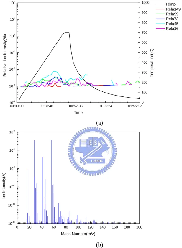
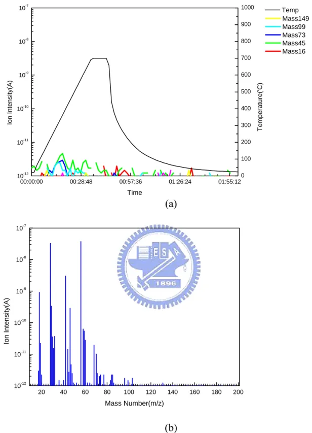
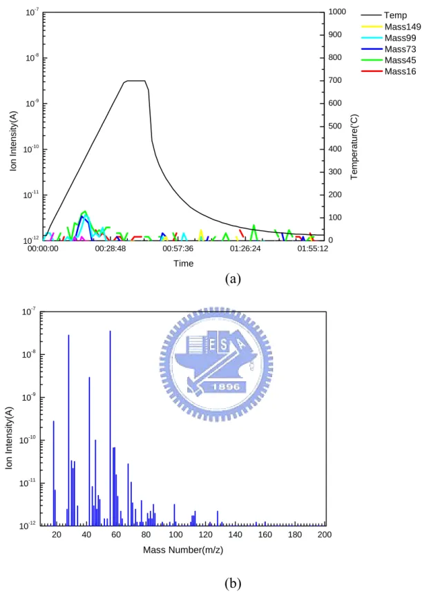
(39) 2. 1000. 10. Temp Rela149 Rela99 Rela73 Rela45 Rela16. 900 1. 800 700. 0. 10. 600 -1. 500. 10. 400 -2. 10. 300. Temperature('C). Relative Ion Intensity(%). 10. 200. -3. 10. 100 -4. 0. 10 00:00:00. 00:28:48. 00:57:36. 01:26:24. 01:55:12. Time. Ion Intensity(A). (a) 10. -7. 10. -8. 10. -9. 10. -10. 10. -11. 10. -12. 0. 20. 40. 60. 80. 100. 120. 140. 160. 180. 200. Mass Number(m/z). (b) Fig. 2-9. TDS-APIMS analysis for unexposed sample: (a) Time depend ion intensity plot, (b) Mass spectrum at temperature = 336℃.. - 25 -.
(40) 2. 1000. 10. Temp Rela149 Rela99 Rela73 Rela45 Rela16. 900 1. 800 700. 0. 10. 600 -1. 500. 10. 400 -2. 10. 300. Temperature('C). Relative Ion Intensity(%). 10. 200. -3. 10. 100 -4. 10 00:00:00. 00:28:48. 00:57:36. 01:26:24. 0 01:55:12. Time. Ion Intensity(A). (a) 10. -7. 10. -8. 10. -9. 10. -10. 10. -11. 10. -12. 0. 20. 40. 60. 80. 100. 120. 140. 160. 180. 200. Mass Number(m/z). (b) Fig. 2-10. TDS-APIMS analysis for CB_PTFE filter sample: (a) Time depend ion intensity plot, (b) Mass spectrum at temperature = 336℃.. - 26 -.
(41) 2. 1000. 10. Temp Rela149 Rela99 Rela73 Rela45 Rela16. 900 1. 800 700. 0. 10. 600 -1. 500. 10. 400 -2. 10. 300. Temperature('C). Relative Ion Intensity(%). 10. 200. -3. 10. 100 -4. 0. 10 00:00:00. 00:28:48. 00:57:36. 01:26:24. 01:55:12. Time. Ion Intensity(A). (a) 10. -7. 10. -8. 10. -9. 10. -10. 10. -11. 10. -12. 0. 20. 40. 60. 80. 100. 120. 140. 160. 180. 200. Mass Number(m/z). (b) Fig. 2-11. TDS-APIMS analysis for CB_GF filter sample: (a) Time depend ion intensity plot, (b) Mass spectrum at temperature = 336℃.. - 27 -.
(42) 2. 1000. 10. Temp Rela149 Rela99 Rela73 Rela45 Rela16. 900 1. 800 700. 0. 10. 600 -1. 500. 10. 400 -2. 10. 300. Temperature('C). Relative Ion Intensity(%). 10. 200. -3. 10. 100 -4. 0. 10 00:00:00. 00:28:48. 00:57:36. 01:26:24. 01:55:12. Time. Ion Intensity(A). (a) 10. -7. 10. -8. 10. -9. 10. -10. 10. -11. 10. -12. 0. 20. 40. 60. 80. 100. 120. 140. 160. 180. 200. Mass Number(m/z). (b) Fig. 2-12. TDS-APIMS analysis for CR sample: (a) Time depend ion intensity plot, (b) Mass spectrum at temperature = 336℃.. - 28 -.
(43) 0. 2. Current Density, J (A/cm ). 10. CB_PTFE (24 hrs) Unexposed tox= 5 nm. -2. 10. -4. 10. -6. 10. -8. 10. -10. 10. -12. 10. 0. 2. 4. 6. 8. 10. 12. 14. 16. 14. 16. Electrical Field, E (MV/cm) (a). 0. 2. Current Density, J (A/cm ). 10. CB_GF (4hrs) Unexposed. -2. 10. tox= 5 nm. -4. 10. -6. 10. -8. 10. -10. 10. -12. 10. 0. 2. 4. 6. 8. 10. 12. Electrical Field, E (MV/cm) (b) Fig. 2-13. J-E curves of MOS capacitors: (a) PTFE filter and (b) Glass-fiber filter. - 29 -.
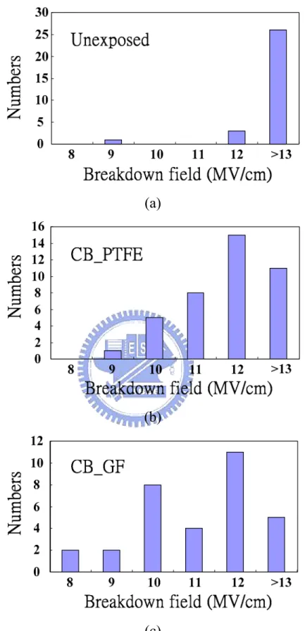
(44) (a). (b). (c) Fig. 2-14. Breakdown field distribution of MOS capacitors: (a) Unexposed samples, (b) PTFE filter, and (c) Glass-fiber filter.. - 30 -.
(45) Cumulative Probility (%). 100. tox= 5 nm. CB_PTFE 2. 80 Area = 200 x 200 µm. @ 4MV/cm. 60 40. Unexposed CB_GF. 20 0 -10 10. -9. -8. 10. -7. 10. 10 2. Leakage Current Density (A/cm ) Fig. 2-15. Cumulative probability of leakage current density under different exposure environments.. - 31 -.
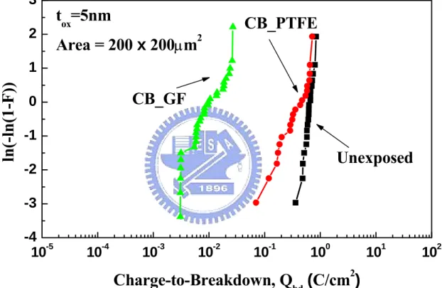
(46) 3 2. tox=5nm. CB_PTFE. 2. Area = 200 x 200µm. ln(-ln(1-F)). 1. CB_GF. 0 -1. Unexposed. -2 -3 -4 -5 10. -4. 10. -3. 10. -2. 10. -1. 10. 0. 1. 10. 10 2. Charge-to-Breakdown, Qbd (C/cm ) Fig. 2-16. Qbd Weibull plot of MOS capacitors under different exposure environments.. - 32 -. 2. 10.
(47) CHAPTER 3 Study on the Degradation of Air Filter in Cleanroom with Acid Vapor Corrosion. 3.1 INTRODUCTION The cleanness of a cleanroom environment must be tightly controlled to achieve high-yield and high-performance ULSI manufacturing [23]-[26]. Recently developed filters, such as HEPA and ULPA filters, effectively eliminate traditional contamination [27]. However, the controllability of airborne molecular contamination (AMC) using present cleanroom technologies has not yet been validated because AMC is a kind of atomic or molecular level gas-phase contamination like organic and inorganic ones. In the near future, especially in the nanodevice era, contamination by organic compounds, inorganic ions and trace doping impurities in air in a cleanroom may dominate the characteristics, reliability, and even yield of devices [28], [29]. Acid vapor generated from the cleaning process is another important issue. Most commercial ULPA filters are made of glass-fiber, which may corroded in an acid vapor environment. Contaminants in a ULPA filter corroded by acid vapor will be released into the cleanroom air and adsorbed onto the surface of wafers, degrading the manufactured devices. Technologies for eliminating AMC from the manufacturing environment must be developed to solve these problems completely. Therefore, the development of a new filter material, which has minimal AMC and is resistant to acid vapor corrosion, is important to the fabrication of high-performance devices. In this study, the performance of the PTFE and the glass-fiber ULPA filters in HF vapor. - 33 -.
(48) environment were investigated. PTFE fiber is considered to be resistant to acid vapor corrosion and it is a good material from which to fabricate ULPA filters. The kinds of AMC and the effects of AMC on devices exposed in the clean bench in a HF vapor environment were examined to elucidate the impact of filter material on device characteristics. The results indicated that the PTFE ULPA filter can provide a better cleanroom environment than a commercial glass-fiber ULPA filter.. 3.2 EXPERIMENTS A specially controlled and fabricated clean bench (CB) was set up in a cleanroom of class 10k. Figure 3-1 schematically depicts the CB. Cleanroom air, from the air inlet of the CB, was initially filtered through a filter module that included inorganic and organic ion chemical filters, before flowing through the main filter, which was designed to be changeable. Two main filters were used, the NEUROFINE PTFE filter (PTFE) and the glass-fiber ULPA filter (GF). The air flow rate and turnover rate inside the CB were set to 0.4 m/s and 5 %, respectively. The exposure experiments were conducted in a 1ppm HF vapor environment. 3.2.1 Evaluation of AMC through Air Sampling Figure 3-2 presents the air sampling tools, Impinger and TENAX, which were equipped with a flow meter and a pump. The flow rate and sampling time of Impinger were 2 L/min and 24-72 hrs while those of TENAX were 100 mL/min and 5 hrs. Impingers collected mainly both metals and boron elements. These were analyzed using an inductively coupled plasma mass spectrometer (ICP-MS). Organic substances were collected by a TENAX (a kind of absorbent) tube, and quantitatively analyzed by gas chromatograph mass spectrometer (GC-MS). The air in the CR was also analyzed for comparison. Table 3-1 summarizes the air sampling experimental conditions.. - 34 -.
(49) 3.2.2 Evaluation of AMC through Wafer Sampling The AMC absorbed on the surfaces of actual 6” P-type (100) Si wafers was analyzed for each filter module. After standard RCA cleaning, wafers were divided into two parts, and exposed to the air in the CR and the CB for 24-72 hrs. The metal contaminants on these wafer surfaces were analyzed using total reflection X-ray fluorescence (TRXRF), while the organic contaminants were analyzed by thermal desorption system–atmospheric pressure ionized mass spectrum (TDS-APIMS). For comparison, the contamination of a wafer not exposed to any environment was evaluated as a control. Table 3-2 is the summary of wafer sampling experimental conditions. 3.2.3 Evaluation of AMC through Electrical Characterization Metal oxide semiconductor (MOS) capacitors were prepared to investigate the effects of AMC on device characteristics. The active region was first defined on a 6” P-type (100) Si wafer by LOCOS process, and then a 40 nm-thick sacrificial oxide layer was formed by thermal oxidation. This sacrificial oxide layer was subsequently removed, and the wafers were further cleaned by RCA cleaning before exposure. After they had been exposed in the CB for 4-72 hours, a 5 nm-thick oxide layer was grown on each wafer by dry thermal oxidation, and an aluminum gate electrode was finally deposited and patterned. The process flow was shown in Fig. 3-3. These samples were used to evaluate the electrical characteristics. Other samples with the additional thermal annealing step after the exposure experiment were used to evaluate the surface doping concentration and the process flow was shown in Fig. 3-4. The Exposure experiments were conducted in a 1 ppm HF vapor environment. Unexposed control samples were also prepared using the same fabrication procedure. Finally, the electrical characteristics including leakage current density distribution, charge to breakdown (Qbd) and doping concentration were measured through the MOS capacitor using a HP4156 - 35 -.
(50) semiconductor parameter analyzer.. 3.3 RESULTS AND DISCUSSION 3.3.1 Pre- and Post-corroded Fiber Structure in HF Vapor Environment Figure 3-5 shows the fiber structure of PTFE-fiber and glass-fiber after the HF vapor corrosion. The pre- and post-corroded fiber structure of PTFE did not reveal any difference and this meant the PTFE-fiber was resistive for HF vapor. On the contrary, the fiber structure of glass-fiber shown in Fig. 3-5(b) displayed the serious degradation in HF vapor environment. The glass-fiber was inevitable to be corroded due to the strong reduction of HF to glass. It is worthy to notice that the corrosion of glass-fiber may release the boron and organic contaminants contained in glass-fiber ULPA filter, thus causing the degradation of device characteristics. Therefore, the PTFE ULPA filter is suitable to be used in acid vapor environment. 3.3.2 Air Sampling Results in HF Vapor Environment Figure 3-6 is the ICP-MS analysis results of metals and boron for different filter modules in HF vapor environment. The PTFE and the glass-fiber ULPA filter can effectively filter the metals including Na, K, Ca, Mg and Al. The CB with the PTFE and the GF ULPA filter, however, showed higher concentration of Fe ions than CR. It was suggested that the steel construction of clean bench corroded by HF vapor, releasing the Fe ions to air. Besides, the CB with GF filter showed large concentration of boron than the CB with PTFE filter. This may due to the corrosion of glass-fiber in HF vapor, releasing the boron atoms contained in glass-fiber as mentioned above. The detail analysis results of ICP-MS are listed in Table 3-3. The organic compounds were considered to be another contamination the glass-fiber will release in HF vapor. Figure 3-7 shows the analysis results of GC/MS. It was found that all the - 36 -.
(51) organic contaminants were removed in the CB with PTFE filter. But for the CB with GF filter, high concentration of organic contaminants appeared. According to our study in Chapter 2, these organic contaminants may come from the binder in GF ULPA filter. In HF vapor environment, the degradation of glass-fiber will release more organic contaminants as show in Fig. 3-7. Table 3-4 shows the detail analysis results of GC/MS. 3.3.3 Wafer Sampling Results in HF Vapor Environment Metal contaminants on wafer surface exposed in the CB in HF vapor environment were quantified by TRXRF analysis. As shown in Fig. 3-8, the densities of metal on different wafers are compared and the detail data are shown in Table 3-5. The “Unexposed” sample refers to a wafer treated only by RCA cleaning and unexposed to air before analysis. On each wafer, five points were analyzed and the averages of the results at these points were compared. The wafer exposed in cleanroom showed higher metal density than the wafers exposed in CB with PTFE or GF filter. This result proved the better filtration efficiency of both PTFE and GF ULPA filter. The Fe ion was previously observed to have high concentration in air sampling; however, in the wafer sampling it showed low concentration. This might be the metals usually adhered to the particles and hence the low particle concentration in the CB with ULPA filter showed low concentration of metals. Next, the intensity of organic contaminants on the wafer exposed in CB in HF vapor environment was evaluated using TDS-APIMS. Figure 3-9 to Fig. 3-12 compares results for different samples. The concentrations of each specifies of organic contamination of the CR sample greatly exceeded that of the CB sample, revealing that the wafer surface exposed in the CR does absorb much organic contamination. Here, mass numbers m/z = 16, 45, 73, 99, 149 were chosen. Contamination peaks at m/z = 16, 45, 149 often come from the outgassing of oil based plasticizers, which are widely used in plastic products of the cleanroom, such as - 37 -.
數據

+7
相關文件
The passages in these reading books are written to help you read faster.. Most learners of English read slowly, but with a little practice, they can read as fast as many
Listen - Check the right picture.?. How are
Practice with your teacher - Listen and repeat Happy Birthday, Jane!.
Practice with your teacher - Show and tell Hi, Mike.. How
Do you want bacon and eggs?.
It’s (between/next to) the church and the
Listen - Check the right picture striped hat polka dotted hat.. Which hat do
Play - Let’s make a big family How many people are in your family1. Write it
