國立交通大學
國立交通大學
國立交通大學
國立交通大學
電子工程學系
電子工程學系
電子工程學系
電子工程學系 電子研究所碩士班
電子研究所碩士班
電子研究所碩士班
電子研究所碩士班
碩
碩
碩
碩 士
士
士
士 論
論
論
論 文
文
文
文
利用低熱預算製程改善碳化矽電
利用低熱預算製程改善碳化矽電
利用低熱預算製程改善碳化矽電
利用低熱預算製程改善碳化矽電
容介面能態密度
容介面能態密度
容介面能態密度
容介面能態密度
Improvement of 4H-SiC MIS Capacitor
Interface State Density by Low Thermal Budget
Processes
研究生
研究生
研究生
研究生:
:
:翁茂元
:
翁茂元
翁茂元
翁茂元
指導教授
指導教授
指導教授
指導教授:
:
:崔秉鉞
:
崔秉鉞
崔秉鉞 教授
崔秉鉞
教授
教授
教授
中華民國一
中華民國一
中華民國一
中華民國一 O 一
一
一年
一
年
年七
年
七
七月
七
月
月
月
利用低熱預算製程改善碳化矽電容介面能態密
度
Improvement of 4H-SiC MIS Capacitor Interface
State Density by Low Thermal Budget Processes
研究生:翁茂元 Student : Marvin-Ueng
指導教授:崔秉鉞 Advisor : Bing-Yue Tsui
國立交通大學 電子工程學系 電子研究所
碩士論文
A thesis
Submitted to Department of Electronics Engineering & Institute of Electronics College of Electrical Engineering and Computer Science
National Chiao Tung University in Partial Fulfillment of the Requirement
for the Degree of Master in
Electronic Engineering 2012
Hsinchu, Taiwan, Republic of China
i
利用低熱預算製程改善碳化矽電容介面能態密
度
研究生:翁茂元 指導教授:崔秉鉞
國立交通大學電子工程系 電子研究所碩士班
摘要
碳化矽因為具有寬能隙以及高熱傳導係數,適合用來製作高功率元件。但是 碳化矽的金氧半場效電晶體(MOSFET)的製作仍有很大的改善空間,如通道載子 移動率的提升是個很重要的課題。氧化層與碳化矽基板之間的高介面能態密度 (大於1012 cm-2)是造成低載子移動率的主因,且既有的閘極氧化層製程都需要 1300以上的高溫氧化及退火,才能得到可接受的閘極氧化層。本論文研究利用低 熱預算製程來降低介面能態密度,比較多種低熱預算製程對各項電性參數包含介 面能態密度、介電層崩潰電場分布的影響,並探討不同的製程條件與介面能態密 度的關係。 我們利用直接低溫(1050 ℃)濕氧氧化的條件當作本論文介面能態密度的參 考上限,理論上氧化厚度越薄介面能態密度越小,研究發現濕氧30分鐘介面能態 密度就達到飽和,原因是溫度不夠高使得一氧化碳(CO)不容易擴散到氧化層表面。 高溫(1300 ℃)一氧化二氮直接氧化的條件做為本論文介面能態密度的參考目標。 在距離導帶(conduction band) 0.4 eV的介面能態密度,低溫濕氧大約是5x1011cm-2eV-1,而高溫一氧化二氮為4.67x1010 cm-2eV-1,有將近十倍的差距。。
一氧化二氮(N2O)或阿摩尼亞(NH3)低溫(1100 ℃)爐管退火可以些微改善介
面能態密度,兩種製程的疊加可以更進一步改善介面能態密度,在距離導帶0.4
潰電場但仍有較寬的電場分佈,可見一氧化二氮退火可以改善氧化層的品質,但 是對於碳化矽基板不平整所造成的局部電場加強導致的提早崩潰,作用不大。增 加一層低壓化學氣相沈積的氮化矽層可以明顯提高崩潰電場並改善崩潰電場分 佈,推測是因為氮化矽和二氧化矽層的缺陷不容易疊對,故不易形成導通路徑。 氨氣電漿處理可以大幅改善介面能態密度,但是在電漿處理過後會產生0.5-1 V的平帶電壓的偏移,此負電荷的產生機制,尚不明瞭。電漿功率在150瓦跟200 瓦有相同的改善趨勢,五分鐘比兩分鐘來的好,十分鐘即達到飽和。200瓦介面 能態密度略高於150瓦,可能是主因是功率太高產生額外的缺陷,而100瓦功率不 夠高即使時間加長到十五分鐘還是不如150瓦十分鐘的效果好。以化學氣相沈積 製程製作介電層堆疊的方法有最低的熱預算,但是介面能態密度高於直接濕氧的 條件,所以需要進一步退火處理。崩潰電場分佈很廣,推測原因是第一層的氧化 層的品質不好,其中機制尚待探討。最後,我們以高溫量測萃取深能帶的介面能 態密度,發現各種介面能態密度改善製程的有效範圍大約是在靠近導帶0.2-0.8 eV區間,對於1 eV以下的介面能態無明顯改善效果。 二次離子質譜儀縱深分析顯示高溫(1300 ℃)一氧化二氮直接氧化的試片, 在二氧化矽/碳化矽介面有氮堆積現象,其它試片則無。推測氮在二氧化矽中不 易擴散,如果先成長純二氧化矽,再進行氮處理,如果製程溫度不夠高,氮無法 到達二氧化矽/碳化矽介面,故介面能態的改善效果不佳。 在所有低預算製程改善中,適當的氨氣電漿處理能達到較低的介面能態密度, 其數值大約是1.37 x1011 cm-2eV-1,但是介面能態密度還是高出本論文最低參考值 三倍(高溫一氧化二氮氧化),且氨氣電漿處理的熱預算太低,只有氫可鈍化介面 能態,推測氫鈍化只對淺能帶的介面能態有效,對0.5 eV以上的介面能態無效。 如果要達到更低值,在新製程開發出來之前,高熱預算的製程還是的無法避免。
iii
Improvement of 4H-SiC MIS Capacitor Interface
State Density by Low Thermal Budget Processes
Student: Marvin-Ueng Advisor: Bing-Yue Tsui
Department of Electronics Engineering
Institute of Electronics
National Chiao Tung University
Abstract
Silicon carbide (SiC) is suitable for fabricating high power semiconductor devices because of its wide band-gap and high thermal conductivity. Unfortunately, low channel mobility occurs on the 4H-SiC MOSFETs due to the high SiO2/SiC
interface state density. How to reduce interface state density is an important issue. In this thesis, several low thermal budget processes to reduce interface state density are evaluated. Electrical parameters including interface state density and breakdown field distribution are analyzed. The effect of process conditions on interface state density is also discussed.
The low temperature (1050 ℃) wet oxidation sample set provides the higher bound reference of the interface state density (Dit) in this thesis. It is expected that the
shorter oxidation time would result in lower interface state density. However, it is observed that lots of carbon clusters saturate on the 0.5 hr wet oxidation sample. It is suspected that the oxidation temperature is not high enough for the diffusion of CO. The interface state density of the wet oxidation sample set is around 5x1011 cm-2eV-1
at Ec-E = 0.4 eV. High temperature (1300 ℃) N2O oxidation sample sets the lower
bound reference of Dit. The Dit value of this sample is 4.67x1010 cm-2eV-1 and is 10
times lower than that of the wet oxidation samples.
Low temperature (1100 ℃) post-oxidation annealing, with the N2O annealing or
NH3 annealing, can improve the interface quality separately. The N2O annealing and
NH3 annealing have superimposed effect the Dit can be improved to 2.92 x10¹¹
cm-2eV-1 at Ec-E = 0.4 eV. N2O annealing can improve breakdown field but the
breakdown field variation is still large. These results indicate that N2O annealing can
improved oxide quality but the early breakdown due to the rough SiC surface cannot be changed. Samples with Si3N4 capping have tight breakdown field distribution
because weak spots in the wet oxide do not coincide with the weak spot in the nitride layer so that early breakdown could be suppressed because current path is hard to form.
NH3 plasma treatment can improve Dit effectively but a 0.5~1 V positive shift of
flat-band voltage compared to wet oxidation sample is observed on all of the plasma treated samples. The trends of interface improvement by plasma treatment at 150 W and 200 W are similar. The interface state density decreases as the plasma treatment time increases from 2 minutes to 5 minutes and gradually saturates as the plasma treatment time increases to 10 minutes. At the same plasma treatment time, 200 W results in slightly higher interface state density than 150 W. It is suspected that higher plasma energy produces additional interface defects due to the stronger radiation. The 100 W 15 min sample has higher Dit than 150 W 10 min. It is thus concluded that 150
W 10 minutes is the optimized condition. Lower energy cannot passivate interface states effectively even if 15 min treatment.
v
required. Dielectric stacks sample exhibits wide breakdown field variation. It is suspected that the quality of the bottom PECVD oxide is too poor. Finally, to extract deep level interface states, high temperature measurement would be required. It is observed that the Dit improvement occurs only in the range of Ec-E = 0.2-0.8 eV. As
Ec-E > 1 eV, there is no Dit improvement on all the samples.
Secondary ion mass spectroscopic analysis shows nitrogen pile-up at the SiO2/SiC interface on the sample HT. This phenomenon is not observed on the other
samples. It is suspected that the diffusion of nitrogen radicals in SiO2 is slow. If
nitrogen incorporation is processed after SiO2 growth, there are not sufficient nitrogen
radicals can reach the interface at low thermal budget processes.
Although suitable NH3 plasma treatment achieves the lowest interface state
density among these low thermal budget samples, Dit = 1.37x1011 cm-2eV-1, this value
is still 3 times higher than the lowest bound reference. Furthermore, the thermal budget of the plasma treatment is too low. Only hydrogen can passivate the interface states. It is suspected that hydrogen can only passivate shallow level interface states and does not affect the interface states deeper than 0.5 eV. To achieve very low interface state density, novel low thermal budget processes must be developed. Otherwise high thermal budget process is still unavoidable.
誌
誌
誌
誌謝
謝
謝
謝
研究所生活即將進入尾聲,在這兩年當中,無論是在課業知識、製程技巧或 是研究方法都習學到許多,過程中雖遭遇些許瓶頸,也靠著大家的幫助使我能度 過難關,自己也成長了許多,在此獻上由衷感謝。 首先最感謝的便是指導教授 崔秉鉞老師,在培養研究生的能力上非常用心, 從實驗規劃到分析實驗上的數據到最後論文的寫作都耐心地指導我並詳加討論, 在作學問的態度方面,積極嚴謹且追根究底的態度,對於我日後思考與做人處事 有莫大的幫助。 實驗方面則感謝交大奈米中心與國家奈米元件實驗室所提供的製程機台,還 有感謝曾經幫助過我的技術員們,另外,還有合作夥伴工研院電光所奈米技術組 這邊研究經費以及碳化矽試片的提供,使我的實驗能夠順利進行。 再來感謝實驗室的大家,元宏學長及嶸健學長在實驗製程、訓練機台、電性 量測、元件物理上的討論與幫助,使我突破了實驗以及數據分析上的瓶頸,還有 感謝實驗室同學炫滋、子瑜、克勤、高銘鴻、孫銘鴻在修課以及機台訓練上的互 相協助,也感謝罩哥、璽允學長、暄美學姊、崇德、哲儒、雪君、翰奇、泰源、 國丞、昕翰、立偉、致弘和易瑾帶來實驗室的歡笑。 最後要感謝我的父母與妹妹對我的支持,也謝謝父母的栽培以及生活上無微 不至的照顧,讓我能無後顧之憂的進行研究,並朝自己的目標前進。 再次由衷的感謝以上諸位的幫忙,使我論文能夠順利完成。
vii
Contents
Abstract (Chinese)………..…. i
Abstract (English)……….……. iii
Acknowledgements……….vi
Contents………...vii
List of Tables………ix
List of Figures………...x
Chapter 1 Introduction ……….……….…..1
1-1 History of Semiconductor Power Devices ………....………….……1
1-2Overview of Wide Band-gap Materials ……….…..……..……….3
1-3Silicon Carbide (SiC) Crystals………...……….….…….……...4
1-4Oxidation Issues of SiC……...……….…..………..5
1-5Motivation……….…….…….……….8
1-6Thesis Organization……….……..………..……….9
Chapter 2 Experiments……….………...15
2-1 MIS Capacitor Fabrication……….…….……….……...………..15
2-2 Electrical Characterization………...……….……….17
2-3 Material Analysis……….……….….……21
Chapter 3 Results and Discussion………..……….………26
3-1 1050 ℃ Wet Oxidation……….………...…………..…..26
3-2 High Temperature Oxidation………..….………..29
3-3 N2O and NH3 Post-Oxidation Annealing………..………….……....30
3-4 NH3 Plasma Treatment………..……….……..……….……32
3-6 High Temperature Measurement………..…...…..34
3-7 Summary of Interface State Density Characteristic………..………37
Chapter 4 Conclusion and Future Works………..…..….……….…..68
4-1 Conclusion……… ….…….…………..………68
4-2 Future Works……….…….…………..……….70
References……….…….……….………..……...72
ix
List of Tables
Chapter 1
Table1-1 Electrical properties parameters of wide band-gap semiconductors …...….10
Chapter 2
Table2-1 Main processes conditions of wet oxidation samples and high temperature
N2O………...………..21
Table2-2 Main processes conditions of NH3 and N2O post oxidation annealing
samples………..………...21 Table2-3 Main processes conditions of NH3 plasma treatment samples………..………21
Table2-4 Main process condition of dielectric stacks……….………22
Chapter 3
Table3-1 The electrical properties of all of the wet oxidation samples are summarized ………..………39 Table3-2 The electrical properties of high temperature N2O sample is summarized...39
Table3-3 The electrical properties of all of N2O and NH3 post-oxidation annealing are
summarized.………..……..……….………..…..40 Table3-4 The electrical properties of all of NH3 post oxidation plasma treatment are
summarized………..……40 Table3-5 The electrical properties of dielectric stacks sample is summarized………41
List of Figures
Chapter 1
Fig.1-1 Application region apply in power devices. IGBT and MOSFET are mainly used in automotive for high frequency application. SCR and GTO are mainly used in high power applications [6]………..………….10 Fig.1-2 History trend of semiconductor power devices [7]……….…….………...….11 Fig.1-3 Theoretical limits of on resistance and breakdown voltage in Si, SiC, and GaN material [11]………..………..11 Fig.1-4 Close-packed sphere model shows three distinct layers (A, B, C) .The first carbon sheet defines a hexagonal plane which is labeled as A. The next bi-layer can be placed on the first sheet ‘valleys’ and is denoted as B or C. [13]………...………..12 Fig.1-5 3C-SiC is the very only 100% cubic polytype exhibiting a strict
zinc-blende-type structure while 2H-SiC represents the only 100% hexagonal polytype of silicon carbide structure (wurtzite-type structure)...12 Fig.1-6 Crystal structures of the two most important SiC polytypes 4H- and 6H-SiC. We can see the Si-terminated face (0 0 0 1) and the C-terminated face (0 0 0 -1) [13]………..……….13 Fig.1-7 There are four Miller Indices (a1 a2 a3 c) in hexagonal structure [13]…….…13
Fig.1-8 Two symmetry atoms (A and B) is described with 3 Miller indices (a1 a2 c),
and 4th Miller Indices (a1 a2 a3 c)………14
Chapter 2
xi
Fig.2-2 Hi-lo CV curve obtained from MOS capacitor………..….….24 Fig.2-3 Time constants versus band-gap plot is at difference temperatures. Horizontal line is interface states extraction region with several methods [37]…..…….24 Fig.2-4 Schematic energy-band diagrams of current transport mechanism. The numbering (1)-(3) is related to current transport path. Where (1) is Fowler-Nordheim tunneling, (2) is Schottky emission, and (3) is Poole-Frenkel emission. EC, EF, EV, and EFM are the conduction band edge,
Fermi level, valence band edge, and Fermi level of Al, respectively……….25
Chapter 3
Fig.3-1 Thickness of wet O2 1050 ℃ as a function of oxidation time. Thickness is
determined by accumulation capacitance (Cox)……….….………....42
Fig.3-2 Thickness (X)-oxidation time (t) plot is fitted by a second order polynomial. The τ value can be extracted by the second order polynomial fitting…..……….……...42 Fig.3-3 Thickness (X) as a linear function of (t+τ)/X. The slope is parabolic rate
constant (B) and intercept is (A).………..……….…43 Fig.3-4 C-V characteristics of sample W5. It is observed that the C-V curves shift
toward negative voltage axis with the decreasing of measurement frequency.………...………..……..43 Fig.3-5 Interface state density characteristic of wet oxidation samples are
summarized.………..……….………44 Fig.3-6 Current density versus electric field (J-E) characteristics of the sample W1..44 Fig.3-7 Breakdown field distributions of only wet oxidation samples. The samples
with thinner oxide, W0.5, W1, and W2, exhibit wide distribution of breakdown field while the samples W3 and W5 have tighter breakdown field
distribution……….………..45 Fig.3-8 (a) SiC surface roughness root mean squire (RMS) value of sample W0.5. The
value of sample W0.5 is 0.65 nm. (b) SiC surface roughness root mean squire (RMS) value of sample W5. The value of sample W5 is 0.576 nm.…….….46 Fig.3-9 (a) The ln (J/E2) against 1/E plot of Fowler-Nordheim linear fit with varying oxidation time. (b) The ln (J/AT2) against E1/2 plot of Schottky-emission (SE) linear fit with varying oxidation time. (c) The ln (J/E) against E1/2 plot of Frenkle-Poole (FP) linear fit with varying oxidation time………...47 Fig.3-10 Barrier heights extract from Fowler-Nordheim tunneling (FN), Schottky
emission (SE), and Frenkle-Poole (FP) as the function of wet oxidation time. The theoretical barrier height is 2.7eV for FN and SE………...48 Fig.3-11 Dielectric constants extract from Frenkel-Poole (FP) and Schottky emission (SE) as the function of wet oxidation time. The theoretical dielectric constant is 3.9……….………..49 Fig.3-12 High-low CV characteristic of sample HT………49 Fig.3-13 The extracted interface state density of sample HT and the sample W5…...50 Fig.3-14 Breakdown field distributions of sample HT and sample W5……….…..…50 Fig.3-15 Cross sectional TEM micrograph of sample NOH (W1 + N2O + NH3+
Si3N4)………..………..51
Fig.3-16 The high frequency C-V characteristics of sample W1, N (W1 + N2O), NH
(W1 + NH3 + Si3N4), NOH (W1 + N2O + NH3 + Si3N4) and HT are
compared…..….………...51 Fig.3-17 The interface state density of sample W1, N (W1 + N2O), NH (W1 + NH3 +
Si3N4), NOH (W1 + N2O + NH3 + Si3N4) and HT are extracted by hi-lo
xiii
Fig.3-18 Current density versus electric field (J-E) characteristic of sample (a) N (W1 + N2O), (b) NH (W1 + NH3 + Si3N4), (c) NOH (W1+ N2O + NH3 +
Si3N4)………..…53
Fig.3-19 Breakdown field distributions of sample W1, N (W1 + N2O), NH (W1 + NH3 + Si3N4), NOH (W1 + N2O + NH3 + Si3N4) ..……….…….54
Fig.3-20 High-low CV characteristic of sample P150.10.……….………..…55
Fig.3-21 Flat-band voltage distributions of high frequency CV of NH3 plasma treatment samples………..……….………..55
Fig.3-22 Interface state density at Ec-E = 0.4 eV characteristic of sample W5, P100.10, P100.15, P150.2, P150.5, P150.10, P200.2, P200.5, and P200.10 are compared.………..………...56
Fig.3-23 Breakdown field distributions of W5 and all NH3 plasma treatment samples.………56
Fig.3-24 High-low CV characteristic of sample ONO………...57
Fig.3-25 Interface state density characteristic of sample ONO and W5………..57
Fig.3-26 Breakdown field distribution of sample ONO………...……58
Fig.3-27 The high frequency C-V characteristics of sample NOH (W1 + N2O + NH3 + Si3N4) at various temperatures. CV negative shift because the work function difference of Al and 4H-SiC is decreased with temperature up.………..………....….58
Fig.3-28 Quasi-static frequency CV characteristic of sample NOH (W1 + N2O + NH3 + Si3N4) measured at 298 K and 523 K.………….………....………..59
Fig.3-29 Interface state density of sample NOH (W1 + N2O + NH3 + Si3N4) measured at various temperatures.…...…59
Fig.3-30 Interface state density of sample P150.10 measured at various temperatures……….….……….……60
Fig.3-31 Interface state density of sample HT measured at various temperatures………..……..………...60 Fig.3-32 The full range interface state density of sample NOH, P150.10 and HT are
compared……….………...61 Fig.3-33 (a) The SIMS profile of the HT sample was obtained from instrumentation
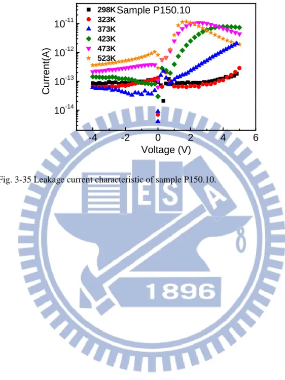
center at NTHU. (b) The SIMS profile of the NOH sample was obtained from MA-TEK. Nitride was removed before SIMS analyze. (c) The SIMS profile of the P150.10 sample was obtained from instrumentation center at NTHU……….………..62 Fig.3-34 Quasi-static frequency CV characteristic of sample P150.10 measured at different temperatures………..………..………...63 Fig.3-35 Leakage current characteristic of sample P150.10………..………..64 Fig.3-36 (a) High low CV of sample P150.10 at 523 K and mobile ion is calculated by
TVS method (b) Sample P150.10 is bias and temperature stress. Temperature is 473 K and bias is ±1.33 MV/cm. The stress time is 30 minutes. ……….….……….65 Fig.3-37 Sample NOH is bias and temperature stress. Temperature is 473 K and bias
is ±1 MV/cm. The stress time is 30 minutes……….…….66 Fig.3-38 High low CV of sample W5 at 523k and mobile ion is calculated by TVS
method………66 Fig.3-39 Interface state densities of representative samples in this thesis are
1
Chapter 1
Introduction
1-1
History of Semiconductor Power Devices
Power semiconductor devices have been developed for several decades. Although the fabrication of power device is on germanium substrate in the beginning, most of the common devices uses silicon as the main substrate currently. The power thyristor, also named silicon controlled rectifier (SCR), introduced in 1950s has high blocking voltage and good ability to handle high current, but the operation speed is low [1]. The other issue for thyristor is hard to turn off. Gate turn-off thyristor (GTO) can turn off device easily by the gate signal but still has low operation frequency and needs complex driving circuit.
Bipolar junction transistor (BJT) which appeared in 1960s provides a solution to the relative low switching speed in thyristor. However, there are several problems in BJT. First, it needs substantial base current to drive so the power dissipation increases in device. Second, when the base-collector junction becomes reverse-biased, BJT requires time to recombine minority carrier in the base and collector which limits the switching speed [2-3]. Third, the avalanche effect in BJT may destroy the device during turn-off operation. In the 1970s, power MOSFET which provides much faster switching speed with low application voltage was developed for power integrated circuits. In order to operate at high voltage, we must reduce the doping concentration to increase the length of the drift region. In this case, the on-resistance drastically increases and causes high power dissipation in the on-state [4.5]. In the 1980s, high performance insulated gate bipolar transistor (IGBT) was proposed. This device has high operation speed in MOSFET and high power in BJT. This advantage makes
IGBT a mainstream of power device since 1990s. Fig.1-1 shows the application region of power devices. IGBT and MOSFET are mainly used in automotive for high frequency application. SCR and GTO are mainly used in high power applications [6]. Fig.1-2 shows the history of semiconductor power devices [7].
The power semiconductor devices have broadened application in power supply automotive, aerospace electronics, TFT-LCD, and so on for several decades. The most common power devices are made of silicon, because silicon is low cost and has mature fabrication technology. But it is forecasted that silicon power devices would be replaced by the devices using wide band-gap substrates at very high power. There are several reasons for limiting the application of silicon power devices.
1. Low breakdown voltage
The impact ionization energy is proportional to the band-gap width, so avalanche breakdown occurs easily with low band-gap width.
2. The high on–resistance (Ron)
For high voltage applications, we must reduce the doping concentration of the drift region to lower the electric field. As the doping concentration decreases and the drift region length increases, thus the series resistance also increases.
3. High reverse leakage current
P-N junction leakage current is proportional to the intrinsic carrier concentration (ni). As shown in eq. (1-1), the band-gap increases and then ni decreases. The off-state
current can effectively reduce as shown in eq. (1-2) [8].
n = eq. (1-1) where ni is the intrinsic carrier concentration (cm-3), Nc is conduction band effective
density (cm-3) and Nv is valence band effective density (cm-3), EG is the band-gap, k is
3
JL= +q eq. (1-2)
where ni is the intrinsic carrier concentration (cm-3), W is the width of the depletion
region (cm), τe is the lifetime of electrons in the depletion region (s), Nd is the
concentration of donor atoms (cm-3), Dh is the diffusion constant of holes in the n-type
region (cm2/s), and τh is the lifetime of holes.
4. Low operation temperature
The band-gap of Si is 1.12 eV. This low value indicates that Si has much higher intrinsic carrier concentration at high temperature than wide band-gap materials. The operation temperature of Si power devices is limited to 150 ℃, because the large leakage current induced by the thermal-generation of electron-hole pairs. Si devices are not suitable for harsh environment.
1-2
Overview of Wide Band-gap Materials
As mention above, Si power devices reach their theoretical limits at high voltage and high temperature application. The wide band-gap materials, such as SiC and GaN, have attracted more and more attention in high power electronics. Fig.1-3 shows the theoretical limits of Si, SiC and GaN. Some important material parameters of wide band-gap semiconductors are listed in Table 1[9]. The band-gap of SiC and GaN is 3.26 eV and 3.39 eV, respectively. Such a wide band-gap allows operation at temperatures higher than 300 ℃. Since SiC has higher breakdown field than Si, SiC can achieve higher breakdown voltage with the same doping concentration. On the other hand, to sustain the same breakdown voltage, SiC devices allow thinner and higher doping drift region. Consequently, higher on-state current density can be conducted and the device area can be reduced. Although GaN has higher carrier mobility than SiC so that higher on current density and lower on resistance can be
achieved in GaN device, SiC has higher thermal conductivity than GaN so that SiC is more suitable at high power and high temperature environment. In addition, GaN usually grows by heteroepitaxy. The substrate such as Si and sapphire are usually used. The cost and quality of GaN crystal growth are issues. GaN is used for blue laser diode and high power microwave device [10-11]. Furthermore, the high defect density in GaN substrate is a big problem. The threading dislocation induces leakage current and limits the ability to produce high power density devices. As discussed above, the excellent electrical and material properties of SiC allow it to be fabricated as power devices.
1-3
Silicon carbide (SiC) Crystals
SiC is composed of silicon and carbon. SiC possesses more than 170 stack sequences known as polytypes. Each sheet of the SiC bi-layer is composed of one Si atom and one carbon atom [12]. Each C atom is bonded with 4 Si atoms. As shown in Fig.1-4 [13], The first carbon sheet defines a hexagonal plane which is labeled as A and The next bi-layer can be placed on the first sheet ‘valleys’ and is denoted as B or C. The packing sequence for HCP is ABAB and that for FCC is ABCABC. Figs.1-5 and 1-6 show the most common polytype stacking sequence in SiC [13]. The name of polytypes consists of number and letter. The number represents the periodicity of the stacking number. The letter represents the structure of polytypes (C=cubic, H= hexagonal, R=rhombohedral). For example, 3C-SiC represents stacking periodicity of ABC and cubic structure. There are four Miller indices (a1 a2 a3 c) in the wurtzite
structure (HCP) such as 4H-SiC (0 0 0 1) .The picture is shown in Fig.1-7. If we describe two symmetry atoms (A and B in Fig.1-8) with 3 Miller indices (a1 a2 c), the
5
index which can label the two atoms as (1 -1 0 0) and (1 0 -1 0) for lattice symmetry. The common used polytypes are 6H-, 4H-, and 3C-SiC. Different SiC polytypes have the same chemical and mechanical properties, but the band-gap and mobility are quite different. The band-gap values of SiC polytypes depend on percentage of hexagonality. The band-gap width of the 3C-SiC (0% hexagonal) is 2.39 eV which differs from the 3.33 eV of the 2H-SiC (100% hexagonal) [14]. We can see the Si-terminated face (0 0 0 1) and the C-terminated face (0 0 0 -1) in Fig.1-6. The two faces are different in oxidation rate and thus different MOS device properties. The 4H-SiC are more often used than the others because of its high breakdown field and high carrier mobility. The 3C-SiC has a smaller band-gap and lower breakdown field but higher mobility than the 6H-SiC. High quality 3C-SiC epi-layer can be grown on Si so that the wafer cost can be reduced.
Although SiC has good electrical properties such as high electron velocity, chemical inert, high breakdown field, and high carrier mobility, some MOSFET fabrication issues exist. First, dopant diffusion in SiC is very slow even at very high temperature so that ion implantation method must be employed. After ion implantation, very high temperature annealing (~1700 ℃) is required to activate dopants. Second, the oxidation rate of SiC is very low. Moreover, the poor SiO2/SiC
interface quality needs to be improved. The oxide reliability at high field and high temperature also needs more investigations.
1-4
Oxidation Issues of SiC
As mentioned above, SiC has superior electrical properties and can produce low on resistance and high blocking voltage power devices. SiC is the only one compound semiconductor that can be thermally oxidized directly, which is similar to the Si
technology. The power MOSFET is an important device for two reasons. First, it has higher switch speed and low power loss than BJT because MOSFET has no minority carrier storage effect. Second, it also has large safe operation area (SOA) for automotive application. The early SiC power MOSFET was reported in 1995 with UMOSFET structure [15]. The trench corner is easily to breakdown, so the breakdown voltage is only 260 V. In order to eliminate the corner breakdown, the DMOSFET structure was reported in 1997 [16]. The breakdown voltage was improved to 760 V. The LDMOSFET with a long lateral drift region can achieve a breakdown voltage of 2.6 kV [17]. Moreover, a RESURF technology combined with LDMOSFET structure to reduce surface field has been reported in literature [18]. In the present, there are several commercialized SiC devices such as Schottky Barrier Diode (SBD), Junction Barrier Schottky Diode (JBSD), and MOSFET. A 1200 V power MOSFET has been commercialized recently [19]. Unfortunately, the low channel mobility in the range of 5–40 cm/V-s occurs on the 4H-SiC MOSFET due to the higher SiO2/SiC interface states density [20]. The large amount trapped charges at
the SiO2/SiC interface results in Coulomb scattering and degrades channel mobility.
The usually measured SiO2/SiC interface states density exceeds 1012 1/cm2/eV, which
is 100 times higher than the SiO2/ Si interface.
The SiC oxidation mechanism obeys the following chemical reaction [21]. SiC + 1.5 O2 → SiO2 + CO
There are several steps for SiC oxidation. First, molecular oxygen transports to the SiO2 surface and then diffuses toward SiO2/SiC interface. Second, molecular oxygen
reacts with SiC forming SiO2 and the product (CO) diffuses out of the SiO2. The
unreacted carbon and undiffused CO residue at the SiO2/SiC interface that cause the
7
(POA) in NO or N2O ambient at high temperature for a long time. During the POA
process, N atoms incorporate to the SiO2/SiC interface and form the Si-N and C-N
bonds to passivate the interface states. NO annealing can be more effective in improving Dit than N2O annealing. Because NO is a toxic gas, it is impractical to use
NO [22-23]. Some researchers used high dielectric constant (high-κ) dielectrics to replace SiO2 [24]. The electric field in high-κ dielectrics is lower than that in the
low-κSiO2 at the same effective thickness. However, the conduction band offset
between high-κand SiC is lower than that between SiO2 and SiC because of the
higher dielectric constant the lower energy band-gap. The carrier tunneling barrier reduces and leakage current increases [25].
POCl3 [26], NH3 [27] and H2 [28] annealing have also been reported in literature.
Although POCl3 annealing can achieve lower Dit than NO annealing, the increase of
positive charges in oxide after annealing causes apparent flat-band voltage shift. H2
annealing exhibits little improvement on Dit and the best result occurs at 800 ℃.
Above 800 ℃, H2 annealing does not further reduce Dit. NH3 and N2O annealing do
not reduce Dit to acceptable level [29]. In addition to these POA methods, the
oxidation in sodium (Na) environment can reduce Dit and achieved channel mobility
to above 150 cm2/Vs. Unfortunately, there are many Na mobile ions in oxide [30]. High doping concentration (>>1015 cm-3) n-type SiC substrate has been used to enhance oxidation rate [21]. This enhancement is due to the doping-induced lattice mismatch. However, the oxide quality degrades due to this mismatch. To enhance oxidation rate, preamorphization by ion implantation has been proposed [31]. The oxidation rate of amorphous SiC is comparable to that of Si so that the low temperature oxidation can be achieved. However, the wide carbon transition region occurs between the crystal SiC and SiO2, as the temperature is not high enough to
1-5
Motivation
The post-oxidation treatment methods in recently literatures are discussed in the previous section. Most of the methods need high temperature and very long annealing process. In this thesis we try to compare different types of low thermal budget processes (<1100 ℃) and the best process for the lowest interface state density is identified. The sample set of low temperature wet oxidation is the high bound reference of interface state density in this thesis since lots of carbon clusters during long time oxidation do not have enough time to diffuse out [32].The current transport mechanisms of the wet oxide samples are also investigated The 1300 ℃ N2O
oxidation sample provides the lowest bound reference of interface states density in this thesis.
Three sets of samples are used to compare with reference samples. First, post-oxidation annealing (N) is performed. We want to understand if NH3 and N2O
annealing have superposition effect or not. Second, the post-oxidation ammonia plasma treatment method has the lowest thermal budget but a few literatures used this method on SiC MIS capacitor [33]. We want to investigate the interface passivation effect with various times and powers of plasma. We also want to know the limitation of plasma treatment with high power and long treatment time. The optimum treatment condition would be found. Third, in order to avoid C transition layer at the SiO2/SiC
interface during thermal oxidation, we try to deposit plasma enhanced chemical vapor deposition (PECVD) oxide and High-κ material on SiC. We obtain large effective oxide thickness (EOT) with dielectric stacks.
High temperature measurement is performed because we want to extract deep level interface state density. We describe the details reasons for high temperature measurement in the next chapter. Mobile ion measurement is also performed in this
9
thesis.
1-6
Thesis Organization
The first chapter is the introduction including fundamental properties of power devices, wide band-gap materials, and SiC crystals. Then, the oxidation issues and known post-oxidation treatment methods are discussed. The second chapter shows the experimental procedure, electrical measurement conditions, and material analyses.
The third chapter is the experimental results and discussion. Various gate dielectrics are divided into 5 categories. They are wet oxidation (W), high temperature N2O oxidation (HT), post-oxidation annealing (N, NH, and NOH), dielectric stack
(ONO), and post-oxidation ammonia plasma treatment (P). Electrical properties such as interface state density and oxide breakdown field are discussed. The high temperature electrical characteristic and material analysis results are also discussed. Finally, the interface states density characteristic of the representable samples are summarized. The last chapter is the conclusions and future works of this thesis.
Table 1-1 Electrical properties parameters of wide band-gap semiconductors [9].
Si 3C-SiC 6H-SiC 4H-SiC GaN
Eg (eV) 1.12 2.3 2.9 3.2 3.39 Ec (MV/cm) 0.3 2 2.5 3 5 Vsat (107 cm/s) 1 2.5 2 2 2 µn (cm2/V-sec) 1450 1000 415 950 1000 r 11.7 9.6 9.7 10 8.9 λ λ λ λ (W/cmK) 1.3 5 5 5 1.3
Fig.1-1 Application region apply in power devices. IGBT and MOSFET are mainly used in automotive for high frequency application. SCR and GTO are mainly used in high power applications [6].
11
Fig.1-2 History trend of semiconductor power devices [7].
Fig.1-3 Theoretical limits of on resistance and breakdown voltage in Si, SiC, and GaN material [11]
1990
1980
1970
1960
1950
Bipolar trans (small power)
Bipolar trans (med power) MOS transistor
IGBT diode
thyristor
Fig.1-4 Close-packed sphere model shows three distinct layers (A, B, C) .The first carbon sheet defines a hexagonal plane which is labeled as A. The next bi-layer can be placed on the first sheet ‘valleys’ and is denoted as B or C. [13].
Fig.1-5 3C-SiC is the very only 100% cubic polytype exhibiting a strict zinc-blende-type structure while 2H-SiC represents the only 100% hexagonal polytype of silicon carbide structure (wurtzite-type structure) [13]
13
Fig.1-6 Crystal structures of the two most important SiC polytypes 4H- and 6H-SiC. We can see the Si-terminated face (0 0 0 1) and the C-terminated face (0 0 0 -1) [13].
Fig.1-8 Two symmetry atoms (A and B) is described with 3 Miller indices (a1 a2 c),
15
Chapter 2
Experiments
2.1
MIS Capacitor Fabrication
Simple metal-insulator-semiconductor (MIS) structure was fabricated. The substrate is an n-type (0 0 0 1)-oriented 4H-SiC epi-wafer. The lightly-doped n-type epi-layer is 11-µm-thick and is doped by N to a concentration of ND = 3-6 x1015 cm-3.
First, a standard RCA clean was performed. Various gate dielectrics were formed by various processes as listed in Tables 2-1, 2-2, 2-3, and 2-4. Aluminum was deposited by thermal evaporation process and patterned by typical lithography process to be gate electrode. The gate area ranges from 1x10⁻³ cm-2 to 1x10⁻⁴ cm-2. The dielectrics on the backside of the samples were wiped by wet processes followed by aluminum deposition to form contact. All samples were annealed at 400℃ for 30 min in N2
ambient. The MIS structure is shown in Fig.2-1. The detailed processes of the various gate dielectrics are explained as follows. Gate dielectrics can be divided into 5 categories. They are wet oxidation (sample W), high temperature N2O oxidation
(sample HT), post-oxidation nitridation annealing (samples N, NH and NOH), dielectric stack (ONO), and post-oxidation ammonia plasma treatment (sample P). 1. Wet Oxidation
The gate dielectrics of sample W0.5, W1, W2, W3, and W5 were grown by wet oxidation process at 1050 ℃ for 0.5, 1, 2, 3, and 5 hr, respectively. The oxidation recipe is shown in Table 2-1. These samples are used to extract the parabolic rate constant (B) and the linear rate constant (B/A) of thermal oxidation of SiC according to the Deal-Grove model [21]. This sample set also provides the higher bound
reference of the interface state density (Dit) because low temperature thermal
oxidation would result in a large amount of carbon clusters at the SiO2/SiC interface
[34].
2. High Temperature N2O Oxidation
The gate dielectric was grown at 1300 ℃ in N2O ambient. This sample provides
the lower bound reference of Dit in this work and is labeled as sample HT. The process
condition is listed in Table 2-1.
3. NH3 and N2O post-oxidation annealing
The gate dielectric of sample N was grown by wet oxidation at 1050 ℃ for 1 hr followed by an N2O annealing at 1100 ℃ for 1 hr. Sample NH has the same wet
oxide as sample N but the post-oxidation annealing was performed in NH3 ambient at
1100 ℃ for 1.5 hr in a low-pressure chemical vapor deposition (LPCVD) system. After annealing, temperature went down to 800 ℃ and a 50-nm-thick Si3N4 layer
was deposited for 5 minutes at 180 mTorr using SiH2Cl2 and NH3 as precursors in the
same LPCVD system. The expected nitride thickness is 50 nm. Sample NOH also has a wet oxide grown at 1050 ℃ for both N2O and NH3 annealing were performed in
sequence after oxidation. After annealing, Si3N4 was deposited with the same
condition for sample NH. This sample is mainly used to investigate whether the NH3
and N2O annealing has superimposed effect. The process conditions are listed in Table
2-2.
4. NH3 plasma post-oxidation treatment
The NH3 plasma treatment method is common used in Silicon process but only
few literatures have been reported on SiC application [33]. The gate dielectric of this sample set was grown by wet oxidation at 1050 ℃ for 5 hr. After oxidation, samples were exposed to NH3 plasma at different powers and periods at 300 ℃. The gas flow
17
250 Pa. The sample ID has the form of PA.B where A represents power in Watt and B represents period in minute. The process conditions are listed in Table 2-3.
5. Dielectric stack
We tried to deposit dielectric on SiC by CVD method in order to avoid C transition layer at SiO2/SiC interface due to oxidation. The gate dielectric of sample
ONO has an oxide/nitride/oxide structure. The sandwiched nitride layer has higher dielectric constant than oxide and thus can allow thicker physical thickness but remains the same effective oxide thickness. The first oxide layer was deposited at 350
℃ using TEOS as precursor to a thickness of 10 nm in a plasma-enhanced chemical
vapor deposition (PECVD) system. Then, a post-deposition annealing in pure O2
ambient at 800 ℃ was performed for 30 min to densify the PECVD oxide. The Si3N4 layer was deposited in a LPCVD system to 57-nm-thick. The top oxide layer
was deposited with the same deposition condition of the bottom oxide layer. The top layer acts as a barrier layer to block carrier injection from the metal gate due to the higher band-gap offset between metal/SiO2 [35]. The expected effective oxide
thickness is 50 nm. The process condition is listed in Table 2-4.
2.2
Electrical Characterization
Both capacitance-voltage (C-V) and current-voltage (I-V) characteristics of the MIS capacitors were measured. The high frequency C-V characteristics were measured by a precision impedance meter of model Agilent 4284A at 10 kHz with voltage swept from +5 to -4 V. The quasi-static C-V and I-V characteristics were measured by a semiconductor parameters analyzer of model Agilent 4156C. The voltage ramping rate for the quasi-static C-V measurement is 50 mV/sec.
capacitance (Cox). The Hi-Lo C-V method is common used to extract the interface
state density. This method was proposed in 1970 [36]. The concept of the method is calculating the capacitance difference between high frequency (>1 kHz) C-V and low frequency C-V at each bias. The low frequency C-V includes the interface states capacitance (Cit) because the interface states are able to follow the low frequency
signal. The interface states almost can’t follow the high frequency C-V signal so that the Cit is not included in the measure capacitance. Fig.2-2 shows the typical Hi-Lo
C-V curves on MOS capacitor. Since SiC is a wide band-gap material, it is hard to measure deep level traps due to their long respond time at room temperature.The time constant for hole emission from an interface states to valence band in a p-type semiconductor can be written as
τ (E) =
!"# $ %&
$
, eq. (2-1) where '( is the capture cross section for holes, )* is the electron thermal velocity, # is the effective density of states in the valence band, k is Boltzmann's constant, T is the absolute temperature, and E-Ev is the energy of the interface state relative to the
valence band edge. Time constant for hole emission versus E-Ev plot is shown in
Fig.2-3 at different temperatures and different Hi-Lo frequency conditions [37]. The horizontal line in Fig.2-3 shows the cut-off frequency of Dit measurement. Those lines
are used to define energy range of Dit measurement. The Dit value can be actually
measure at room temperature using the Hi-Lo C-V method is about 0.2-0.6 eV away from the conduction band or valence band. If we want to measure deep level traps, rising temperature, bias at inversion, and illumination where interface response times are shorter are common methods used in literature. In this thesis, the measurement temperature is raised to 523 K. We can extract deep level Dit at 1.6 eV away from the
19
energy is
EC − Et = −ψS + Eg/2+ kT ln(ND/ni)/q, eq. (2-2)
where EC is conduction band energy, Et is trap energy, ψS is the band-bending under
gate bias, Eg is the energy gap of 4H-SiC, ND is the doping concentration, ni is the
intrinsic carrier concentration of 4H-SiC, k is the Boltzmann constant and T is the absolute temperature.
The dielectric breakdown field is extracted from the I-V characteristics. The I-V curve is converted to current density-electric field (J-E) plot firstly using following equations:
J = I/AG, eq. (2-3)
E = (VG-VFB)/EOT, eq. (2-4)
where AG, VFB, J, E, and EOT are gate area, flat-band voltage, current density, electric
field in oxide, and effective oxide thickness with respect to SiO2, respectively. The
breakdown field is defined as the electric field at which the current density equals to 10-2 A/cm2.
The J-E plot is also used to identify the current transport mechanism. The Fowler-Nordheim (FN) tunneling, Schottky emission (SE), and Frenkel-Poole (FP) emission are been considered [38].
1. Fowler-Nordheim (FN) tunneling The J-E equation is shown in eq. (2-5).
, eq. (2-5)
where J is F-N tunneling current, E is electric field in oxide, m* is effective electron mass in oxide, φB,FN is barrier height between semiconductor and oxide, and h is
Planck’s constant. The F-N tunneling barrier height (φB,FN) can be extracted from the
( )
− = E q q m E J B h 3 2 4 exp 2 / 3 * 2φ
ln (J/E2) versus 1/E plot. The slope gives barrier height (φB,FN). The current path is
shown in Fig. 2-4(1). 2. Schottky emission (SE)
The J-E equation of Schottky emission is expressed as
eq. (2-6) and
A
*=
,-./∗1
23
,
eq. (2-7)where A* is termed as the effective Richardson constant, J is current density governed by Schottky emission, m* is effective electron mass in oxide, E is electric field in oxide, φB,
ε
I, k and h are Schottky barrier height, dielectric constant, Boltzmann’sconstant, and Planck’s constant, respectively. The SE barrier height (φB,SE) can be
extracted from the ln(J/AT2) versus E1/2 plot. The intercept gives the barrier height (φ
B,SE). The current path is shown in Fig. 2-4(2). The dielectric constant can be extracted
from the plot. This value can be used to confirm if SE is the actual current transport mechanism.
3. Frenkel- Poole (FP)
The J-E equation of the FP emission is shown in eq. (2-8).
, eq. (2-8)
where J is the current density governed by Frenkel-Poole emission, E is electric field in oxide, φB,PF,
ε
I, and k are barrier height, dielectric constant, and Boltzmann’sconstant, respectively. The barrier height (φB,PF) and dielectric constant (
ε
I) can beextracted from the ln(J/E) versus E1/2 plot. The intercept gives barrier height and the slope is related to dielectric constant. The current path is shown in Fig. 2-4(3).
(
)
− − = kT qE q T A J * 2expφ
B /4πε
I(
)
− − = kT qE q E J expφ
B /πε
I21
Mobile ions in gate dielectric were measured in this thesis. First, the bias temperature stress (BTS) method was utilized. We elevated temperature to 473 K and applied around -1 MV/cm constant field for 30 min. Then, sample was cooling down to room temperature and high frequency C-V was measured to extract VFB(-). Second,
sample was applied a +1 MV/cm electric field at 473 K for 30 min. After cooling down to room temperature, C-V was measured to extract VFB(+). The calculation
formula for mobile ion density Qm is shown in eq. (2-9).
eq. (2-9) Another measurement method is triangular voltage sweep (TVS). High frequency and quasistatic C-V characteristics were measured at 523 K. We integrated the area between high frequency and quasistatic C-V to obtain mobile ion value.
2-3
Material Analysis
Several material analysis techniques were used to understand the sample structure and dielectric composition. High resolution transmission electron microscope (TEM) was used to determine the accurate dielectric thickness and the interface roughness. The Energy-dispersive X-ray spectroscopy (EDS) was used to determine the atomic composition of each dielectric layer. Nitrogen may pile up at the SiO2/SiC interface after various nitridation processes to passivate defects and reduce
Dit. Carbon cluster at the SiO2/SiC play important role on the interface quality. The
depth profiles of N and C were measured by secondary ion mass spectrometry (SIMS) using Cs+ as primary ion. The surface roughnesses on SiC surface and on gate dielectric surface were measured by atomic force microscopy (AFM)
) ( ) (+ − − × = acc FB FB m C V V Q
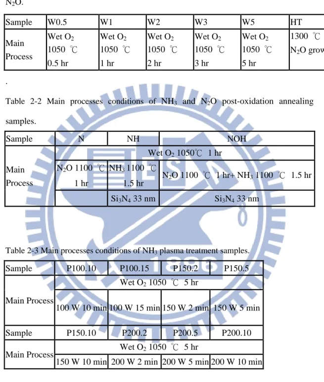
Table 2-1 Main processes conditions of wet oxidation samples and high temperature N2O.
.
Table 2-2 Main processes conditions of NH3 and N2O post-oxidation annealing
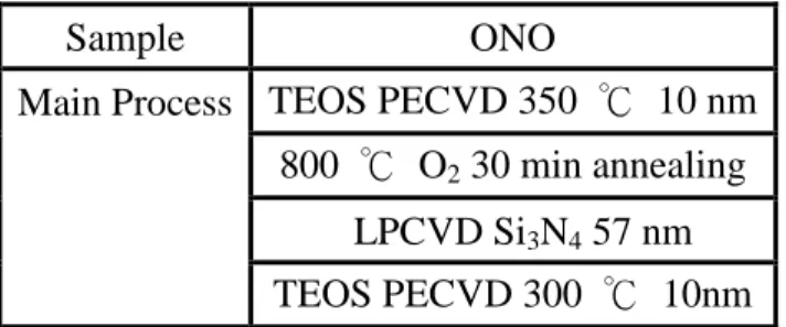
samples. Sample N NH NOH Main Process Wet O2 1050℃ 1 hr N2O 1100 ℃ NH3 1100 ℃ N2O 1100 ℃ 1 hr+ NH3 1100 ℃ 1.5 hr 1 hr 1.5 hr Si3N4 33 nm Si3N4 33 nm
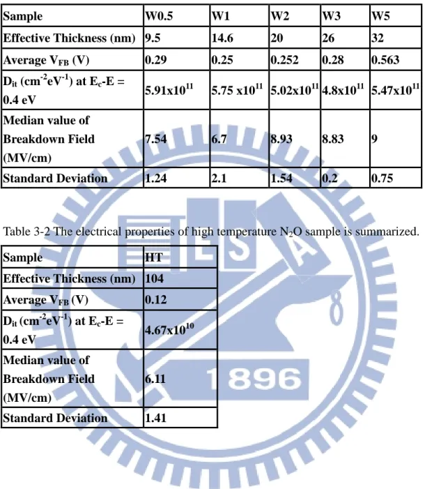
Table 2-3 Main processes conditions of NH3 plasma treatment samples.
Sample P100.10 P100.15 P150.2 P150.5
Main Process
Wet O2 1050 ℃ 5 hr
100 W 10 min 100 W 15 min 150 W 2 min 150 W 5 min
Sample P150.10 P200.2 P200.5 P200.10
Main Process Wet O2 1050 ℃ 5 hr
150 W 10 min 200 W 2 min 200 W 5 min 200 W 10 min
Sample W0.5 W1 W2 W3 W5 HT Main Process Wet O2 1050 ℃ 0.5 hr Wet O2 1050 ℃ 1 hr Wet O2 1050 ℃ 2 hr Wet O2 1050 ℃ 3 hr Wet O2 1050 ℃ 5 hr 1300 ℃ N2O grown
23
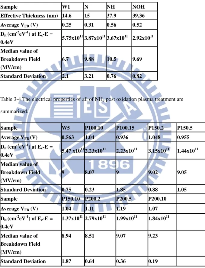
Table 2-4 Main process condition of dielectric stacks.
Fig.2-1 Schematic cross-sectional structures of the MIS capacitors
Sample ONO
Main Process TEOS PECVD 350 ℃ 10 nm 800 ℃ O2 30 min annealing
LPCVD Si3N4 57 nm
TEOS PECVD 300 ℃ 10nm
4H -SiC 350μ m
dielectric
4H -SiC epi -layer 11μm
Al contact
Fig.2-2 Hi-lo CV curve obtained from MOS capacitor
Fig.2-3 Time constants versus band-gap plot is at difference temperatures. Horizontal line is interface states extraction region with several methods [37].
25
Fig.2-4 Schematic energy-band diagrams of current transport mechanism. The numbering (1)-(3) is related to current transport path. Where (1) is Fowler-Nordheim tunneling, (2) is Schottky emission, and (3) is Poole-Frenkel emission. EC, EF, EV, and
EFM are the conduction band edge, Fermi level, valence band edge, and Fermi level of
Chapter 3
Experimental Results and Discussion
3-1
1050 ℃Wet Oxidation
The low temperature direct thermal oxidation is investigated in this thesis firstly. Samples W0.5, W1, W2, W3, W5 were wet oxidize at 1050 ℃ for 0.5 hr, 1 hr, 2 hr, 3 hr, and 5 hr, respectively. The thicknesses of the five samples are 9.5 nm, 14.6 nm, 20 nm, 26 nm and 32 nm in sequence. These thickness values are calculated from the accumulation capacitance (Cox). Thickness as a function of oxidation time is shown in
Fig.3-1. The oxide thickness saturates when the oxidation time becomes larger than five hours. Deal-Grove model is used to calculate the parabolic rate constant (B) and linear rate constant (B/A). The formula is shown in below.
t+τ =
45
+
45 6 , eq.(3-1)
where X is the oxide thickness, τ is the time that consider native oxide, t is the oxidation time. In the initial oxide growth period, the X is very small. The linear term (B/A) dominates. The linear rate constant is related to the reaction between SiC and oxidants. If oxidants diffuse through grown oxide to oxidize the underlying SiC substrate and the product of CO molecules diffuse out of the sample for long term oxidation, the parabolic rate constant (B) dominates the oxidation rate. This constant is determined by the gas diffusivity at grown oxide. The calculation procedures are described in the next paragraph [21].
First, the thickness-oxidation time (t) plot is fitted by a second order polynomial. The τ value can be extracted by the second order polynomial fitting as shown in Fig.3-2. The extracted τ value is 0.43 hr. With the known τ value, we can plot the thickness (x) as a linear function of (t+τ)/x. The slope is parabolic rate constant (B)
27
and intercept is A as shown in Fig.3-3. The parabolic rate constant is around 0.000287
μm2
/h. The linear rate constant is around 0.019μm/h. These two values are much lower than those of silicon oxidation, and the oxidation rate of SiC is quite slow.
The C-V characteristics of sample W5 is shown in Fig.3-4. It is observed that the C-V curves shift toward negative voltage axis with the decreasing of measurement frequency, and the shape of the C-V curves changes slightly at all frequencies. This phenomenon is related to the response of the interface states near conduction band. The deep level interface states can response the DC and AC signal at low frequency since the deep level states have longer trapping and detrapping time constant [39]. Significant separation of the high-low C-V curves indicates that high interface state density exists near conduction band edge.
It is expect that the shorter oxidation time sample has lower interface state density due to fewer carbon cluster formation. The interface state density extracted by the hi-lo C-V method is shown in Fig.3-5. There is no significant difference in interface state density between Sample W0.5, W1, W2, W3, W5. This result indicates that a large amount of carbon clusters have been formed in 0.5 hr at 1050 ℃. The interface state density is around 5x1011 cm-2eV-1 at Ec-E = 0.4 eV. It has been reported
that the interface state density depends on wet oxidation thickness in literature but the oxidation temperature is 1110 ℃ which is higher than our experiment [40]. It is seems that lots of carbon clusters saturate on sample W0.5 because the oxidation temperature is possibly not high enough for the diffusion of CO.
The breakdown characteristic of 13-15 devices was measured on each sample. The breakdown voltage is defined at which the current density J = 10-2 A/cm2. Fig.3-6 shows the current density versus electric field (J-E) characteristics of the sample W1. The samples with thinner oxide, W0.5, W1, and W2, exhibit wide distribution of breakdown field while the samples W3 and W5 have tighter breakdown field
distribution as shown in Fig.3-7. The breakdown field of 8-9 MV/cm is achieved. The reasons for large variation of breakdown field of thinner oxide sample (< 20 nm) are possibly due to surface roughness. If the surface roughness of SiC is large, the electric field is partially enhanced at certain positions. The enhancement is more significant on samples with thinner oxide. The oxides of sample W0.5 and W5 were removed for AFM measurement. The AFM results are shown in Fig.3-8 (a) and Fig.3-8 (b). The root mean squire (RMS) roughness on SiC surface of the two samples are almost the same and the roughness does not depend on oxide thickness. The RMS value of sample W0.5 is 0.65 nm and that of sample W5 is 0.576 nm. Therefore, it is suspected that the surface roughness is the main reason for the early breakdown observed on the thin oxide samples. In summary, although wet oxidation results in high interface state density, the breakdown characteristic is reliable as the oxide is thicker than 26 nm.
The current transport mechanism is investigated by fitting the I-V characteristics with various transport models. The Fowler-Nordheim barrier height (ΦB,FN) is
extracted by eq. 2-5. First, the ln(J/E2) versus 1/E plot in the field of 6~10 MV/cm region is shown in Fig.3-9 (a). The slope gives the barrier height ΦB,FN.This value is
related to the conduction band offset between SiO2 and SiC. The theoretical value of
ΦB is 2.7 eV. The extracted ΦB,FN values are shown in Fig.3-10. The ΦB,FN
decreases as the oxide thickness decreases. The possible reason is the surface roughness of the SiC substrate. The enhanced electric field causes the effective barrier height lowing. Sample W3 and W5 have barrier height larger than 2.7 eV. The reason is still unclear.
The Schottky-emission (SE) mechanism is examined according to eq. 2-6. The ln(J/AT2) versus E1/2 plot is shown in Fig.3-9 (b). The intercept of linear fitting of plot is related to the Schottky emission barrier height (ΦB,SE) and the slope of plot is
29
dielectric constant. The extracted ΦB,SE value is shown in Fig.3-10. These values are
slightly smaller than the theoretical value of 2.7 eV. Dielectric constant extracted by eq. 2-6 is shown in Fig.3-11. Those values are extremely lower than the theoretical dielectric constant of 3.9. Furthermore, the Frenkle-Poole (FP) emission barrier height (ΦB,FP) and dielectric constants are extracted by eq. 2-8. The ln (J/E) versus E1/2 plot
is shown in Fig.3-9 (c). The slope of the ln (J/E) versus E1/2 plot is related to the dielectric constant and intercept of the plot is barrier height. The extracted ΦB,FP
value is shown in Fig.3-10. These values are about 1.8 eV. The extracted dielectric constant is shown in Fig.3-11. The values of sample W0.5 and W1 are close to the theoretical dielectric constant of 3.9 but the other samples have extremely lower dielectric constant.
In summary, FP emission is the main transport mechanism for samples W0.5 and W1 but the mechanisms for samples W2 W3 and W5 are still unclear. The electrical properties of all of the wet oxidation samples are summarized in Table 3-1.
3-2
High Temperature N
2O Oxidation
The gate dielectric of sample HT is grown by the directly oxidation at 1300 ℃ in N2O ambient and is provided by the Industrial Technology Research Institute
(ITRI). The effective oxide thickness is 104 nm. The high frequency and quasi-static C-V characteristics are shown in Fig.3-12. These two C-V curves are very close which implies that the interface state density is very low at conduction band edge. Fig.3-13 compares the extracted interface state density of sample HT with the sample W5. It is clear that the interface state density of sample HT is much lower than that of the wet oxidation sample. The interface state density at Ec-E = 0.4 eV is about 4.67x10¹⁰
The breakdown field distributions of sample HT and sample W5 are shown in Fig.3-14. The breakdown field of sample HT is lower than the sample W5. It is suspect that the lower breakdown field is due to the thick oxide. As the oxide thickness increases, the process induced defects may increase. These defects may percolate to a leakage path so that the breakdown is reduced. The extracted electrical properties of sample HT are summarized in Table 3-2.
3-3
N
2O and NH
3Post-Oxidation Annealing
The gate dielectric of sample N was grown by wet oxidation at 1050 ℃ for one hour followed by N2O annealing for 1 hr at 1100 ℃. This sample is designed to
investigate the low temperature N2O annealing effect. The wet oxide thickness is
around 14.6 nm and the final gate dielectric thickness increases slightly to 15 nm after N2O annealing. The gate dielectric of sample NH was grown by wet oxidation at 1050
℃ for one hour followed by a 1.5 hr NH3 post-oxidation annealing. After that, a
50-nm-thick nitride was deposited. The nitride deposition is used to increase the EOT to around 50 nm without high temperature oxidation. Sample NOH experienced sequential N2O and NH3 post-oxidation annealing. After that, nitride layer was
deposited. The cross-sectional TEM micrograph of sample NOH is shown in Fig.3-15. The actual silicon dioxide layer is around 12.8-nm-thick. A 2~3-nm-thick interfacial layer is formed between the Si3N4 layer and the SiO2 layer. This interfacial layer is
identified as SiON by EDS analysis. The thickness of the Si3N4 layer is around 33 nm.
The high frequency C-V characteristics of sample W1, N, NH, NOH and HT are compared in Fig.3-16. Samples W1 and N exhibit almost identical C-V curves and flat-band voltage. The flat-band voltage does not shift significantly after N2O
31
post-oxidation annealing. The C-V curves of samples NH and NOH are slightly “stretched-out” compared to that of sample W1. The reason will be discussed later.
The interface state density extracted by hi-lo C-V method is shown in Fig.3-17. Either N2O annealing or NH3 annealing can improve the interface quality separately.
Among them, sample NOH has the lowest interface state density except the sample HT. This result indicates that the N2O and NH3 treatment has superposition property.
The values of the interface state density of samples N, NH, and NOH are 3.87 x10¹¹, 3.67 x10¹¹, and 2.92 x1011 cm-2eV-1, respectively, at Ec-E = 0.4 eV. The mechanism of
interface state passivation is related to nitrogen pile up at SiO2/SiC. Possible chemical
reaction of N2O annealing has been proposed in ref [41]. N2O decompose to N2 and
O2 at high temperature.O2 reacts with N2O to form NO. The NO diffusion in SiO2
causes the nitrogen piling up.
The I-V characteristics of samples N, NH, and NOH are shown in Fig.3-18 (a), (b), and (c), respectively, and the breakdown field distribution is shown in Fig.3-19. Although sample N has higher Median breakdown field than sample W1, the breakdown field variation of sample N is similar to that of sample W1. The higher Median breakdown field implies that the oxide quality in bulk is improved by N2O
annealing. The large variation implies that N2O annealing does not smooth the SiC
surface roughness. The Median breakdown field is around 10 MV/cm on sample NH and sample NOH and the distribution is quite tight.
Early breakdown phenomenon occurs on samples W0.5, W1, W2, and N. These samples have thin wet oxide as gate dielectric. No early breakdown is observed on sample NH and NOH. The main difference between these two groups is the nitride deposition. The early breakdown is attributed to some weak spots in the dielectric. If the weak spots in the wet oxide do not coincide with the weak spot in the nitride layer, early breakdown could be suppressed because current path is hard to form. Using gate
![Table 1-1 Electrical properties parameters of wide band-gap semiconductors [9].](https://thumb-ap.123doks.com/thumbv2/9libinfo/8238864.171257/26.892.135.733.142.847/table-electrical-properties-parameters-wide-band-gap-semiconductors.webp)