國
立
交
通
大
學
電子工程學系 電子研究所
博 士 論 文
具備新穎自我對準升高式源/汲極結構之低溫複晶矽薄膜電晶體元件
之開發與寬通道效應之研究
Development of Novel Self-Aligned Raised Source/Drain Structure for
Low-Temperature Polysilicon Thin-Film Transistor and the Study of the
Channel Width Widening Effect
研 究 生:林俊銘
指導教授:張國明 教授
具備新穎自我對準升高式源/汲極結構之低溫複晶矽薄
膜電晶體元件之開發與寬通道效應之研究
Development of Novel Self-Aligned Raised Source/Drain Structure for
Low-Temperature Polysilicon Thin-Film Transistor and the Study of the
Channel Width Widening Effect
研 究 生:林俊銘 Student:Gin-Ming Lin
指導教授:張國明 Advisor:Kow-Ming Chang
國 立 交 通 大 學
電子工程學系 電子研究所
博 士 論 文
A DissertationSubmitted to Department of Electronics Engineering and Institute of Electronics
College of Electrical and Computer Engineering National Chiao Tung University
in partial Fulfillment of the Requirements for the Degree of Doctor of Philosophy
in
Electronics Engineering
February 2008
Hsinchu, Taiwan, Republic of China
具備新穎自我對準升高式源/汲極結構之低溫複晶矽薄膜電
晶體元件之開發與寬通道效應之研究
學生:林俊銘 指導教授:張國明 博士
國立交通大學
電子工程系電子研究所
中文摘要
在這篇論文中我們專注於新的低溫複晶矽薄膜電晶體結構開發,並針對當 通道寬度大於源汲極寬度時,寬通道效應所造成的電流增加做研究與討論。 首先,我們利用傳統熟知之金屬鑲嵌與化學機械研磨技術,用以開發出新 穎之具備自我對準之閘極與增高式源汲極結構之低溫複晶矽薄膜電晶體元件,在 此一結構中,鄰近源/汲極區之通道厚度將增厚,此一特徵將可有效降低元件關 閉時汲極區附近之側向電場,可使此一結構之漏電流相較於傳統共平面結構至少 降低十倍以上。我們更利用 2-D 模擬軟體進一步討論與研究側向電場在不同之通 道深度處之數值變化。 接著,我們利用一次蝕刻或過蝕刻方式製作另一具有自我對準之增高式源 汲極結構的低溫複晶矽薄膜電晶體元件。,此一結構相較於傳統增高式源汲極結 構製作流程而言,可減少一次微影製程,並且製作更簡單。此外,由於利用閘極 區域定義之光阻層作為下層通道區域定義之蝕刻阻擋層,因而此結構之通道寬度 將與閘極區域寬度等寬,並大於源汲極區域之寬度。該特徵將可使此一新穎結構 除了具有與先前開發之增高式源汲極結構相同低的漏電流外,更可提升薄膜電晶 體之驅動電流與增加開關電流比。最後,我們特別針對在通道寬度大於源汲極寬度之條件下薄膜電晶體驅動 電流進行研究。由於現有之金氧半場效電晶體或複晶矽薄膜電晶體之驅動電流物 理模型乃是建立在通道寬度與源汲極寬度等寬之前提條件,因而利用現行之驅動 電流模型,我們並無法解釋薄膜電晶體之驅動電流在通道寬度大於源汲極寬度時 的導通行為並進行預估驅動電流數值。因此,我們利用一具有通道寬度大於源汲 極寬度特性之測試結構,進行薄膜電晶體之驅動電流的研究,並提出一簡單的關 係式,解釋驅動電流與通道長度、通道寬度與源汲極寬度間之關聯性。
Development of Novel Self-Aligned Raised Source/Drain
Structure for Low-Temperature Polysilicon Thin-Film
Transistor and the Study of the Channel Width Widening Effect
Student: Gin Ming Lin Advisors: Dr. Kow-Ming Chang
Department of Electronics Engineering &
Institude of Electronics
National Chiao-Tung University
Hsinchu, Taiwan, R.O.C
Abstract
In this thesis, we concentrate our efforts on new Low-temperature Poly-Si TFT
structure development, and discuss the effect of channel width widening on a Poly-Si
TFT which will occur when the channel width is larger than the source/drain width.
First, we apply the damascene process and Chemical Mechanical Polish (CMP)
Technology to develop a novel TFT structure with a self-aligned gate and raised
source/drain (SAGRSD). In this structure, thick channel regions will be formed near
the source/drain regions, this feature will suppress the lateral electric field near the
drain region to reduce the OFF-state leakage current of the Poly-Si TFT at least one
order of magnitude as comparing to the conventional co-planar Poly-Si TFT. We also
drain region will be reduced by using this novel TFT structure, and discussed the
lateral electric field in different channel depth in thick channel region near the
source/drain regions.
Secondly, we also develop another new low-temperature Poly-Si TFT structure
with self-aligned raised source/drain (SARSD) by one-step etching or over-etching
method. For this new structure, thick source/drain regions and a thin channel region
could be achieved with only four mask steps, which are less than that in conventional
raised SD TFT’s. Moreover, the channel width of the proposed structure would be
larger than its source/drain width. Wide channel width will improve the ON-state
current due to carrier will flow from the source to the drain via new current flow paths
occurred in the side channel region. Therefore, this structure will have the ON-state
current and the ON/OFF current ratio of the Poly-Si TFT, and maintain low OFF-state
leakage current as same as SAGRSD TFT.
Finally, we also find that current physical models for MOS or Poly-Si drain
current are not suitable to explain the behavior of the drain current flow in the channel
region of the SARSD TFT in which the channel width is wider than the source/drain
width. Therefore, we use a test structure to clarify and define the relationship of the
drain current among the channel length, the source/drain width and the channel width
誌
謝
本論文的完成首先要感謝我的指導老師張國明教授,張教授在研究上的指 導確切詳盡,在生活上的關心無微不至,讓我這六年半的博士生活中受益良多, 其次還要感謝桂正楣教授的幫忙與建議,讓我的論文發表更順利。 在完成論文的建立過程中,還要特別感謝實驗室的學長學弟們的幫助:鍾 元鴻學長、楊文誌學長、王敬業學長、朱俊宜同學、趙高毅同學、楊學人學弟、 翁世學學弟、謝孟帆學弟、楊國良學弟、陳正國學弟在實驗上的建議與幫忙;郭 俊銘學弟、林建宏學弟、陳伯寧學弟和黃士軒學弟等在我心情低落時陪我放鬆心 情;感謝交通大學奈米中心(NCTU-NFC)林素珠小姐、徐秀鑾小姐、何惟美小姐 在實驗上的幫忙。 最後謹以此論文現給我的父母親林添福先生與林徐昭美女士,感謝他們在 我求學階段的鼓勵與支持,感謝我的姊姊們的鼓勵,同時也要感謝我的妻子邱玉 如女士與我可愛的女兒林采穎,因為你們的存在,我才能順利完成我的博士論 文,謝謝你們。
Contents
Chinese Abstract………...i
English Abstract……….iii
Acknowledgment……….v
Contents………..vi
Table Captions……….……….. ix
Figure Captions………...x
Chapter 1 Introduction
1.1 Background and Motivation………...1
1.2 Thesis Organization………4
References
Chapter 2
A Novel Low-Temperature Polysilicon Thin-Film
Transistors with a Self-Aligned Gate and Raised
Source/Drain Formed by Damascene Process
2.1 Introduction………..14
2.2 Device Fabrication………15
2.3 Result and Discussion………...17
2.4 Summary………...19
References
Chapter 3
A Novel Four-Mask Step Low-Temperature
Polysilicon Thin-Film Transistors with Self-Aligned
Raised Source/Drain (SARSD)
3.1 Introduction………..34
3.2 Device Fabrication………35
3.3 Result and Discussion………...37
3.4 Summary………...39
References
Chapter 4
Effect of Channel Width Widening on a Poly-Si
Thin-Film Transistor Structure in the Linear Region
4.1 Introduction………..52
4.2 Device Fabrication………54
4.3 Result and Discussion………...55
4.3.1 Simulation Results of the Test Structure ( W
ch> W
sd)
and the Conventional Structure ( W
ch= W
sd)………55
4.3.2 Equivalent Circuit of the Channel Region of the Test
Structure ( W
ch> W
sd) in the Linear Region……….57
4.3.3 Electrical Characteristics of the Test Structure ( W
ch>
W
sd) and the Conventional Structure ( W
ch= W
sd) in
the Linear Region………..58
4.3.4 Relationship among the ON-state Drain Current or the
ON-state Drain Current Gain and the Channel Length,
the Side-Channel Width and the Source/Drain Width
in the Linear Region
………..……….604.4 Summary………...63
References
Chapter 5
Conclusion and Future Works
5.1 Conclusion………78
5.2 Future works……….79
Vita………..…81
T
ABLE
C
APTIONS
Table 2-1
Maximum lateral electric field of the conventional and
proposed TFT structures in the ON-state……….30
Table 2-2
Maximum lateral electric field of the conventional and
proposed TFT structures in the OFF-state………..……….32
F
IGURE
C
APTIONS
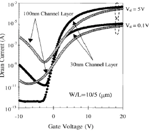
CHAPTER 1Fig. 1-1 Ids – Vgs transfer characteristics of the conventional co-planar TFT with
thicker (100nm) and thinner (30nm) channel thicknesses………..11
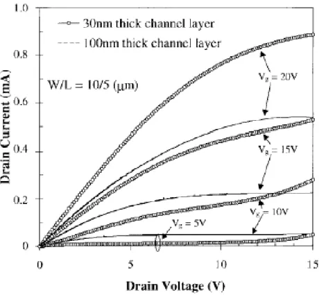
Fig. 1-2 Ids – Vds output characteristics of the conventional co-planar TFT with
thicker (100nm) and thinner (30nm) channel thicknesses………..12
Fig. 1-3 Proposed new RSD TFT structure………..13
CHAPTER 2
Fig. 2-1 (a)-(d) Schematic cross sections of the major fabrication steps of the
proposed n-channel D-SAGRSD TFT………...24
Fig. 2-2 Cross-section view of the proposed D-SAGRSD TFT structure………...25
Fig. 2-3 Ids – Vgs transfer characteristics of the proposed D-SAGRSD TFT and the conventional co-planar TFT……….26
Fig. 2-4 Simulation current flow lines of (a) the conventional co-planar TFT; (b)
the proposed D-SAGRSD TFT………..27
Fig. 2-5 Simulation position of the lateral electric field of the conventional
co-planar TFT……….28
Fig. 2-6 Simulation positions of the lateral electric field of the proposed
Fig. 2-7 Simulated lateral electric field distribution of the proposed D-SAGRSD
TFT and the conventional co-planar TFT in the OFF-state………...31
Fig. 2-8 Ids – Vds output characteristics of the proposed D-SAGRSD TFT and the
conventional co-planar TFT. The insert plots are the Ids – Vds output characteristics of the proposed D-SAGRSD TFT and the conventional
co-planar TFT in the linear region……….33
CHAPTER 3
Fig. 3-1 (a)-(c) Schematic cross section of the major fabrication steps of the
proposed n-channel SARSD TFT………...42
Fig. 3-2 Schematic diagram of the current flow lines of the proposed SARSD
structure………..43
Fig. 3-3 SEM photograph of the proposed SARSD TFT structure………..44
Fig. 3-4 Current flow lines simulated by MEDICI in (a) the conventional co-planar
structure with Lch = 15 µm and Wch = Wsd = 5 µm; (b) the SARSD
structure with Lch = 15 µm, Wsd = 5 µm and Wch = 30 µm………45
Fig. 3-5 Ids-Vgs transfer characteristics of the proposed SARSD TFT in both forward mode(F) and reverse mode(R) and the conventional co-planar TFT,
in which the reverse mode is source and drain electrodes exchanged…...46
conventional co-planar TFT………...47
Fig. 3-7 Ids-Vgs transfer characteristics of the proposed SARSD TFT with different channel widths……….48
Fig. 3-8 Maximum ON-state current and minimum OFF-state leakage current of the
proposed SARSD TFT with various the side channel width, and the
conventional co-planar TFT………...49
Fig. 3-9 OFF-state leakage current of the proposed SARSD TFT with various the
side channel width, and the conventional co-planar TFT measured at
Vgs=-15V and Vds=5V………..50
Fig. 3-10 ON/OFF current ratio of the proposed SARSD TFT with various the
side-channel width, and the conventional co-planar TFT………..51
CHAPTER 4
Fig. 4-1 Schematic top view of the major fabrication steps for the test TFT’s……68
Fig. 4-2 Current flow lines simulated by MEDICI in (a) the conventional structure
with Lch = 1 0 µm and Wch = Wsd = 5 µm; (b) the test structure with Lch
= 3 µm, Wsd = 5 µm and Wch = 30 µm; (c) the test structure with Lch =
10 µm, Wsd = 5 µm and Wch = 30 µm; (d) the test structure with Lch =
10 µm, Wsd = 10 µm and Wch = 30 µm………...69
main-channel resistance; Rs,c is the side-channel resistance)…………...70
Fig. 4-4 (a) Ids-Vgs transfer characteristics; (b) Ids-Vds output characteristics of
the test structure with Lch /Wsd = 1 0 µm /5 µm with different side-channel widths (Wsc) compared with the conventional structure…..71
Fig. 4-5 (a) Ids-Vgs transfer characteristics; (b) Ids-Vds output characteristics of
the test structure of Lch /Wsd = 5 µm / 15 µm with different side channel widths (Wsc) compared with the conventional structure………...72
Fig. 4-6 Distributions of the ON-state drain currents of the test structure with (a)
Wsd = 5µm; (b) Wsd = 1 0 µm as a function of the side-channel width
Wsc……….73
Fig. 4-7 Average values for the ON-state drain current gain Ai of the test structure
with (a) Wsd = 5µm and (b) Wsd = 1 0 µm as a function of the
side-channel width Wsc……….74
Fig. 4-8 Distributions of the ON-state drain current gain Ai of the test structure
with (a) Wsc = 6 µm and (b) Wsc = 1 4 µm compared with channel length
Lch……….75
Fig. 4-9 Distributions of the ON-state drain current gain Ai of the test structure
with (a) Wsc = 6 µm; (b) Wsc = 1 4 µm compared with the ratio of the
Fig. 4-10 Experimental and calculated maximum ON-state drain current for the test
structure with different source/drain widths and different applied drain
biases compared with the channel length Lch, in which solid symbols represent the experimental data and empty symbols represent the
Chapter 1
I
NTRODUCTION
1.1 B
ACKGROUND ANDM
OTIVATIONIn recent years, the broad band networks have been expanding, and mobile information and communication tools have been widely used. The flat panel display (FPD) which acts as a critical interface to connect with people is assembled into those mobile tools, such as cellular phones, personal digital assistants (PDA), digital cameras, notebook PCs, and so on [1.1]. Therefore, the FPD plays an important role in human life. Up to now, the FPD has been replacing the cathode ray tube (CRT) based traditional display. Meanwhile, the current FPD market has been dominated by amorphous silicon thin-film transistors (α-Si TFTs) based active matrix liquid crystal display (AMLCD) [1.2]. However, α-Si TFTs have a low carrier mobility to limit the signal response time, and are with a large and dark area on a panel to limit the resolution. They inherently limit the performance of active matrix displays. In order to overcome these disadvantages, many techniques on low-temperature polycrystalline silicon thin file transistors (LTPS-TFTs) have been proposed to replace α-Si TFTs. LTPS TFTs integrated peripheral driver circuits with AMLCDs have been widely used [1.3], [1.4]. And an average of their carrier mobility is more than one hundred times the mobility of α-Si TFTs. This technology is being considered as the candidate to achieve a system on
panel (SOP) and ultimately sheet computer in the future [1.5], [1.6].
Many technologies for fabricating the high-performance LTPS-TFTs have been extensively investigated, such as methods of α-Si crystallization, defect reduction, and novel TFT structure fabrication.
α-Si crystallization means that an amorphous silicon layer is crystallized into a polycrystalline silicon layer by annealing. The α-Si crystallization is the most important step in the fabrication of LTPS-TFTs. This step is the key process of limiting the thermal budget on large area glass substrates. The performance of LTPS-TFTs is strong dependent on the quality of an active layer. The solid phase crystallization (SPC) [1.7] ~[1.9], metal induced crystallization (MIC) [1.10] ~[1.12], and excimer-laser crystallization (ELC) [1.13] ~[1.15] are the main methods in the fabrication of LTPS-TFTs.
However, whether α-Si films are crystallized by solid phase crystallization (SPC) or by excimer-laser crystallization (ELC), it is hard to avoid existences of grain boundaries in the channel regions for large dimension device. Moreover, existences of grain boundaries and high drain electric field will cause an increase in the leakage current, a variation in the threshold voltage with the drain bias, a kink effect in the output characteristics, and a poor hot-carrier stress endurance [1.16]. These effects can be eliminated by reducing the electric field near the drain region. Therefore, many novel structures are developed to reduce the electric field. For example, the field-induced drain [1.17] ~[1.20], sub-gate coupling structure [1.21] ~[1.24], dual gate structure
[1.25], double-gate structure [1.26] ~[1.28] and lightly-doped drain structure [1.29] ~[1.35]. Unfortunately, most of these structures usually need complicated processes, causing a barrier for being fabricated on a large area glass structure. Therefore, how to simplify the fabrication of high-performance poly-Si TFTs is the most important issue in LTPS TFT-based active matrix displays [1.36].
The well-know El-Mansy/Ko model [1.37] and [1.38] describes the maximum channel electric field for the bulk MOSFET’s as
E
max=(V -V
DS Dsat)/
l
(1.1) Where the characteristic length is given as l
=
s i o x j o xl
ε
t
ε
x
(1.2)and
ε
si andε
ox are the permittivity for Si and SiO2, respectively; is the gate oxide thickness, andox
t
j
x
is the drain junction depth. Hence, it can be concluded that for a given oxide thickness, theE
max can be reduced by increasing the junction depth.Therefore, increasing the drain junction depth is one way of reducing electric field near the drain side. For the conventional co-planar TFT, increasing the channel thickness could increase drain junction depth at the same time. However, it has been reported that increasing channel thickness will not only increase grain-boundary traps, but also reduce the ON-state current and increase OFF-state leakage current, as shown in Fig. 1-1 and 1-2. Therefore, we hope to develop a novel TFT structure, as shown in Fig. 1-3, to suppress the maximum channel electric field by increasing
the junction depth.
1.2 T
HESISO
RGANIZATIONIn this thesis, we concentrate our efforts on new TFT structure development, and discuss the effect of channel wide widening on a Poly-Si TFT which will occur when the channel width is larger than the source/drain width.
Chapter 1 describes the background and motivation. In chapter 2, we apply the damascene process to develop a novel TFT structure with a self-aligned gate and raised source/drain. 2-D simulation tool, MEDICI, is also used to verify that the electric field near the drain region will be reduced by using this novel TFT structure. In chapter 3, another new TFT structure is proposed. For this new structure, thick source/drain regions and a thin channel region could be achieved with only four mask steps, which are less than that in conventional raised SD TFT’s. Moreover, the channel width of the proposed structure would be larger than its source/drain width. Wide channel width will improve the ON-state current due to carrier will flow from the source to the drain via new current flow paths occurred in the side channel region. Therefore, in chapter 4, the effect of channel width widening on a Poly-Si TFT in the linear region are thus studied carefully.
Finally, in chapter 5, a conclusion is given for this thesis, and some future works about this thesis are proposed.
References
[1.1] S. J. Battersby, “System on panel for mible displays,” in Tech. Dig. AMLCD, 2001, pp. 5-8.
[1.2] K. Chung, M. P. Hong, C. W. Kim, and I. Kang, “Needs and solutions of future flat panel display for information technology industry,” in IEDM Tech. Dig.,2002.
[1.3] N. Sasaki, A. Hara, F. Takeuchi, Y.Mishima, T. Kakehi, K. Yoshino, and M. Takei, “High throughput CW-laser lateral crystallization for low-temperature poly-Si TFTs an fabrication of 16 bit SRAMs and 270 MHz shift registers,” in SID Techs. Dig., 2002, pp. 154-157.
[1.4] H. J. Kim, D. Kim, J. H. Lee, I. G. Kim, G. S. Moon, J. H. Huh, J. W. Hwang, S. Y. Joo, K. W. Kim, and J. H. Souk, “A 7-inch full-color low temperature poly-Si TFT-LCD,” in SID’99 Dig., 1999.
[1.5] Yojiro Matsueda, Satoshi Inoue, and Tatsuya Shimoda, “Concept of System on Panel,” in Tech. Dig. AMLCD, 2001, pp. 77-80.
[1.6] K. Kanzaki, “Poly-Si TFT technology for system on glass,” in Tech. Dig. AMLCD, 2001, pp. 71-74.
[1.7] M. K. Hatalis, and D. W. Greve, “Large grain polycrystalline silicon by low-temperature annealing of low-pressure chemical vapor deposited amorphous silicon films,” J. Appl. Phys., vol. 63, pp. 2260-2266, Apr. 1988.
[1.8] T. Yoshida, M. Kinugawa, S. Kanbayashi, S. Onga, M. Ishihara, and Y. Mikata, “Crystallization technology for low voltage operated TFT,” in IEDM Tech.Dig., pp. 843-846, 1991.
[1.9] S. Onga, Y. Mizutani, K. Taniguchi, M. Kashiwagi, K. Shibata, and S. Kohyama, “Characterization of polycrystalline silicon MOS transistors and its film properities,” Jpn. J. Appl. Phys., pt. 2, vol. 21, no. 10, pp. 1472-1478, Oct. 1982.
[1.10] C. Hayzelden, and J. L. Batstone, “Silicide formation and silicon-mediated crystallization of nickel-implanted amorphous silicon thin films,” J. Appl. Phys., vol. 73, pp. 8279-8289, Oct. 1993.
[1.11] Z. Jin, G. A. Bhat, M. Yeung, H. S. Kwok, and M. Wong, “Nickel induced crystallization of amorphous silicon thin films,” J. Appl. Phys., vol. 84, pp. 194-200, July 1998.
[1.12] M. Wong, Z. Jin, G. A. Bhat, P. C. Wong, and H. S. Kwok, “Characterization of the MIC/MILC interface and its effects on the performance of MILC thin-film transistors,” IEEE Trans. Electron Devices, vol. 47, pp, 1061-1067, May 2000.
[1.13] S. D. Brotherton, D. J. McCulloch, J. B. Clegg, and J. P. Gowers, “Excimer-laser-annealed poly-Si thin-film transistors,” IEEE Trans. Electron Devices, vol. 40, pp, 407-413, Feb. 1993.
[1.14] G. K. Giust, T. W. Sigmon, J. B. Boyce, and J. Ho, “High-performance laser-processed polysilicon thin-film transistors,” IEEE Electron Device Lett., vol. 20, pp. 77-79, Feb.
1999.
[1.15] K. Sera, F. Okumura, H. Uchida, S. Itoh, S. Kaneko, and K. Hotta, “High-performance TFT’s fabricated by XeCl excimer laser annealing of hydrogenated amorphous-silicon film,” IEEE Trans. Electron Devices, vol. 36, pp. 2868-2872, Dec. 1989.
[1.16] T. F. Chen, C. F. Yeh, and J. C. Lou, “Investigation of grain boundary control in the drain junction on laser-crystallized poly-Si thin film transistors,” IEEE Electron Device Lett., vol. 24, pp. 457-459, July 2003.
[1.17] H. C. Lin, K. L. Yeh, R. G.. Huang, C. Y. Lin, and T. Y. Huang, “Schottky barrier thin-film transistor (SBTFT) with silicided source/drain and field-induced drain extension,” IEEE Electron Device Lett., vol. 22, pp. 179-181, Apr. 2001.
[1.18] H. C. Lin, C. M. Yu, C. Y. Lin, K. L. Yeh, T. Y. Huang, and T. F. Lei, “A novel thin-film transistor with self-aligned field induced drain,” IEEE Electron Device Lett., vol. 22, pp. 26-28, Jan. 2001.
[1.19] M. C. Lee, S. H. Jung, I. H. Song, and M. K. Han, “A new poly-Si TFT structure with air cavities at the gate-oxide edges,” IEEE Electron Device Lett., vol. 22, pp. 539-541, Nov. 2001.
[1.20] J. Y. Nahm, J. H. Lan, and J. Kanicki, “Hydrogenated amorphous-silicon thin-film transistor structure with the buried field plate,” in IEDM Tech. Dig., pp. 309-312, 1999. [1.21] K. M. Chang, Y. H. Chung, C. G. Deng, Y. F. Chung, and J. H. Lin, “Characterization of
the novel polysilicon TFT with a subgate coupling structure” IEEE Trans. Electron Devices, vol. 49, pp. 564-567, Apr. 2002.
[1.22] C. M. Park, B. H. Min, and M. K. Han, “Novel offset gated poly-Si TFTs with subgate,” IEEE Trans. Electron Devices, vol. 46, pp. 1402-1405, July 1999.
[1.23] K. M. Chang, Y. H. Chung, G. M. Lin, J. H. Lin, and C. G. Deng, “A novel high-performance poly-Si thin film transistor with a self-aligned thicker sub-gate oxide near the drain/source regions,” IEEE Electron Device Lett., vol. 22, pp. 472-474, Oct. 2001.
[1.24] M. Yu, H. C. Lin, G. H. Chen, T. Y. Huang, and T. F. Lei, “Characteristics of polycrystalline silicon thin-film transistors with electrical source/drain extensions induced by a bottom sub-gate,” Jpn. J. Appl. Phys., vol. 41, pp. 2815-2820, May 2002.
[1.25] M. C. Lee, S. J. Park, M. Y. Shin, and M. K. Han, “Characteristics of asymmetric dual-gate poly-Si TFTs for kink current reduction,” in SID Tech. Dig., 2003, pp. 252-255. [1.26] A. Kumar, J. K. O. Sin, C. T. Nguyen, and P. K. Ko, “Kink-free polycrystalline silicon
double-gate elevated-channel thin-film transistors,” IEEE Trans. Electron Devices, vol. 45, pp. 2514-2520, Dec. 1998.
[1.27] S. Zhang, R. Han, J. K. O. Sin, and M. Chan, “Implementation and characterization of self-aligned double-gate TFT with thin channel and thick source/drain,” IEEE Trans. Electron Devices, vol. 49, pp. 564-567, May 2002.
[1.28] S. Zhang, R. Han, J. K. O. Sin, and M. Chan, “A novel self-aligned double-gate TFT technology,” IEEE Electron Device Lett., vol. 22, pp. 530-532, Nov. 2001.
[1.29] P. S. Shih, T. C. Chang, T. Y. Huang, C. F. Yeh, and C. Y. Chang, “Characterization and reliability of lightly-doped-drain polysilicon thin-film transistors with oxide sidewall spacer formed by one-step selective liquid phase deposition” Jpn. J. Appl. Phys., vol. 39, pp. 5758-5762, Oct. 2000.
[1.30] B. H. Min, and J. Kanicki, “Electrical characteristics of new LDD poly-Si TFTstructure tolerant to process misalignment,” IEEE Electron Device Lett., vol. 20, pp. 335-337, July 1999.
[1.31] S. Zhang, R. Han, and M. J. Chan, “A novel self-aligned bottom gate poly-Si TFT with in-situ LDD,” IEEE Electron Device Lett., vol. 22, pp. 393-395, Aug. 2001.
[1.32] K. Y. Choi, and M. K. Han, “A novel gate-overlapped LDD poly-Si thin-film transistor,” IEEE Electron Device Lett., vol. 17, pp. 566-568, Dec. 1996.
[1.33] C. H. Fang, D. H. Deng, S. C. Chang, and Y. M. Tsai, “Fullyself-aligned low-temperature poly-Si TFT process with symmetric LDD structure,” in SID Tech. Dig., 2003, pp. 1318-1321.
[1.34] M. Hatano, H. Akimoto, and T. Sakai, “A novel self-aligned gate-overlapped LDD poly-Si TFT with high reliability and performance,” in IEDM Tech. Dig., pp. 523-526, 1997. [1.35] Z. Meng, T. Ma, and M. Wong, “Suppression of leakage current in low-temperature
metal-induced unilaterally crystalline silicon thin film transistor using an improved process sequence and a gate-modulated lightly-doped drain structure,” in IEDM Tech. Dig., pp. 755-758, 2001.
[1.36] D. H. Kim, P. M. Choi, K. W. Chung, T. Uemoto, and C. W. Kim, “Development of 5’ poly-Si transflective panel by 7-mask process, operated with P-MOS circuit,” in SID Tech. Dig., 2003, pp. 348-349.
[1.37] Y. A. El-Mansy and A. R. Boothroyd, “A simple two-dimensional model for IGFET operation in the saturation region,” IEEE Trans. Electron Devices, vol. 24, p. 254, 1977. [1.38] P. K. Ko, R. S. Muller, and C. Hu, “A unified model for hot-electron currents in
Fig. 1-1 I
ds– V
gstransfer characteristics of the conventional co-planar TFT with
Fig. 1-2 I
ds– V
dsoutput characteristics of the conventional co-planar TFT with
S
G
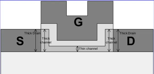
D
Thin channel Thick channel Thick channel Thick Drain Thick DrainChapter 2
A Novel Low-Temperature Polysilicon Thin-Film Transistors
with a Self-Aligned Gate and Raised Source/Drain Formed by
Damascene Process
2.1 I
NTRODUCTIONLow-temperature polycrystalline silicon (LTPS) TFT’s have been widely investigated for several years [2.1]. However, the undesired OFF-state leakage current for a poly-Si TFT is much higher than that of an amorphous TFT. It is well known that the OFF-state leakage current mechanism is the field emission via grain boundary traps due to high electric field in the drain depletion region [2.2]. Thus, suppressing the off-state leakage current by reducing the drain electric field is required. Several methods have been proposed to achieve this purpose, such as offset gated structure [2.3], lightly doped drain structure [2.4] and field induced drain structure [2.5], [2.6]. In the lightly doped offset drain structure, the On-state current is significantly suppressed at the same time [2.7]. In the field induced drain structure, an additional photo masking step is required and unavoidable photo masking misalignment error will occur [2.5], [2.6]. It also has been previously reported that the thick source/drain region not only serves to reduce the lateral electric field, thus maintaining the breakdown voltage [2.8],[2.9], but also to reduce the source/drain series resistance.
Pervious methods used to fabricate such structures with thin active channel and thick source/drain regions, however, are not self-aligned in nature, and require additional masks [2.8],[2.9], when compared to the conventional co-planar TFTs.
In this chapter, a novel four mask steps self-aligned gate RSD Poly-Si TFT structure formed by the damascene process (D-SAGRSD TFT) is proposed. The new device features a thin active channel region and a thick source/drain region. The Gate and RSD regions are self-aligned and no additional mask is needed. Moreover, we use the 2-D numerical simulator MEDICI for device analysis to study the variation of the lateral electric field influenced by device structure in both ON-state and OFF-state. For the sake of simplicity, the single crystalline silicon model already available in MEDICI is used to just estimate the electric field effects of these two Poly-Si TFT structures.
2.2 D
EVICEF
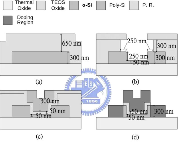
ABRICATIONFig. 2-1 shows the process flow of the D-SAGRSD TFT structure. First, a 300-nm α-Si layer for active region was deposited by low pressure chemical vapor deposition (LPCVD) system using SiH4 at 550°C on 500-nm thermal oxidized silicon wafers. After patterning, the active region was formed using reactive ion etching (RIE) at this mask step. Then, the first (650-nm) plasma enhanced chemical vapor deposition (PECVD) tetraethoxysilane (TEOS) oxide layer was deposited at 350 °C.
Chemical-mechanical polishing (CMP) process was employed to planarize the first TEOS oxide surface, as shown in Fig. 2-1(a). The thickness of the first TEOS oxide above the active region after polishing is about 300-nm. After patterning, the RIE process was used to etch the α-Si layer and then selective BOE etching was used to form a T-sharp gutter, as shown in Fig. 2-1(b). Because the α-Si layer had no stopper layer, the α-Si thin channel region thickness was controlled by etching rate (8.33 Å/sec). Additionally, the α-Si film thickness was determined by Ellipsometer, and the thickness of the thin channel region was accurately controlled, with an error of within ±3% (50 ± 1.5 nm). After etching, the thickness of the active region became 50-nm. After the photoresist was removed, the α-Si film was annealed in nitrogen ambient at 600°C for 24 h to become the poly-Si film. After recrystallization, the etching damages of the channel surface were recovered and the surface roughness is approximately 3 nm. A 50-nm plasma enhanced chemical vapor deposition (PECVD) TEOS gate oxide layer was deposited at 350 °C, and then a 300-nm LPCVD Poly-Si film was deposited. After CMP process was employed to planarize the Poly-Si film surface to form the T-sharp gate as shown in Fig. 2-1(c), the 50-nm TEOS gate oxide and the first TEOS oxide were removed by BOE solution. Then, Gate, Source and Drain regions were formed by ion implantation of Phosphorous(Dose = 5 x 1015 cm-2 at 50 keV) and then activated in nitrogen ambient at 600 °C for 24 h, as shown in Fig. 2-1(d). After the source, drain and gate activation, the second (500-nm) passivation TEOS oxide was deposited by PECVD. Contact holes were opened using wet etching of the passivation oxide layer. A layer of aluminum was then deposited by thermal coater system with
a thickness of 600 nm. After metal patterning, a forming gas anneal is performed at 400°C for 30 min. The total masks of our fabrication processes are four masks, which are less than those of conventional processes in a RSD poly-Si TFT [2.8],[2.9]. For comparison, the conventional co-planar poly-Si TFTs with 50-nm channel thickness were also fabricated in the same run. The total channel length of the proposed TFT is shown in Fig. 2-2.
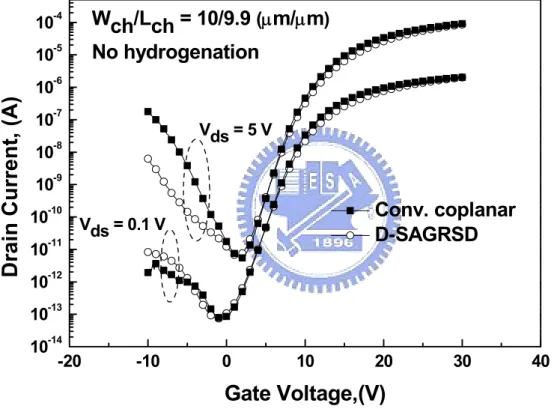
2.3 R
ESULTS ANDD
ISCUSSIONThe Ids-Vgs transfer characteristics of the proposed D-SAGRSD TFT structure compared with the conventional co-planar TFT were shown in Fig. 2-3. It can be observed that, even though the D-SAGRSD TFT has a slightly lower ON-state current and a slightly higher minimum OFF-state current, much lower OFF-state leakage current (Vgs = -10 V and Vds = 5 V) can be also obtained. The proposed TFT has two symmetrical thick channel regions near source and drain sides. These thick channel regions have much more grain boundary traps than the thin channel region, and these grain boundary traps would cause the ON-state current decreasing and minimum OFF-state current increasing. Besides, as shown in Fig. 2-4(a), the current flow lines of the conventional co-planar TFT in the ON-state are uniform distribution in the inversion layer near the oxide/channel interface. However, for the proposed D-SARSD TFT, even most of the carriers can transport in the inversion layer near the oxide/ Poly-Si interface, some carriers still can directly transport to the
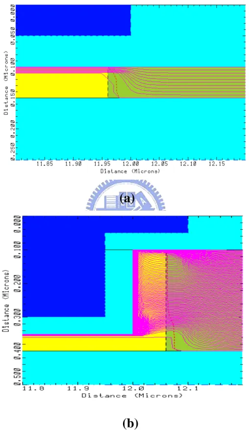
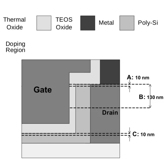
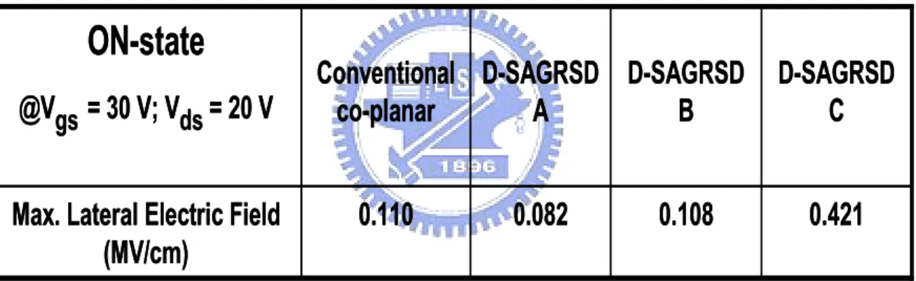
drain region in the thick channel region, as shown in Fig. 2-4(b). This phenomenon may be due to the variation of the lateral electric field in the thick channel region near the drain side. Figs. 2-5 and 2-6 show the simulation positions of the lateral electric field of the conventional co-planar TFT and the proposed D-SAGRSD TFT simulated by MEDICI, respectively. The simulation results of the conventional co-planar TFT and the proposed D-SAGRSD TFT are shown in Table 2-1. It can be observed that the maximum lateral electric field of the proposed D-SAGRSD TFT in the point C of Fig. 2-6 is remarkable larger than that of the conventional co-planar TFT in ON-state. Therefore, we can conclude that, for the proposed D-SAGRSD TFT, carriers in the thick channel region can transport to the drain region via the inversion layer near the oxide/ Poly-Si interface, and directly transport to the drain region due to high lateral electric field near the drain side. Moreover, the proposed TFT would have a higher threshold voltage and a larger sub-threshold swing than those of the conventional TFT due to bad channel control in the corners of the channel and bad oxide/Poly-Si interface of the vertical channel region.
For the OFF-state current measured at higher drain and reverse gate bias (Vds = 5 V, Vgs = -10 V), the main reason of much lower OFF-state current of the proposed D-SAGRSD TFT is that the leakage current is determined by the electron-hole pair generation rate in the depletion region at the drain edge. The pair generation rate is strongly dependent on the number of trap-states in the forbidden gap, lateral electric field and a generation volume of the depletion region [2.10]-[2.12]. Although a thick drain region causes the generation volume of the D-SAGRSD TFT to increase, the
maximum lateral electric field near the drain region of the D-SAGRSD TFT, as shown in Fig. 2-7, is also largely dropped (see Table 2-2) due to thick source/drain regions [2.13]. At higher drain and reverse gate bias (Vds = 5 V, Vgs = -15 V), the leakage current would be due to the thermionic field emission via grain boundary defects [2.14]. Even though the generation volume would be increased, the D-SAGRSD TFT, therefore, would have a lower OFF-state leakage current than that of the conventional TFT because the maximum lateral electric field near the drain region is notably reduced. Fig. 2-8 shows the Ids - Vds curves of the proposed TFT compared with the conventional TFT. In the insert plots, it can be observed that the proposed TFT has a lower source/drain parasitic resistance due to steeper slopes of Ids - Vds of the proposed TFT in the linear region. However, in the saturation region, the ON-state current of the proposed TFT is lower than that of the conventional TFT; it is because the maximum lateral electric field of the proposed TFT is also dropped due to thick source/drain regions (see Table 2-1).
2.4
S
UMMARYIn this chapter, a novel four mask steps n-channel self-aligned gate raised source/drain Poly-Si TFT formed by damascene process was proposed and investigated. Remarkable OFF-state current can be obtained and good ON/OFF current ratio can be maintained for the proposed D-SAGRSD TFT. The self-aligned gate and raised source/drain regions can be formed without the additional
mask step and therefore reduce the lateral electric field near the drain side to suppress the OFF-state current. This new TFT structure may be an attractive device structure for future high-performance large-area device applications.
References
[2.1] I-Wei. Wu, “Low temperature poly-Si TFT technology for AMLCD application,” in Tech. Dig. AMLCD, 1995, pp. 7-10.
[2.2] Jerry G. Fossum, Adelmo Ortiz-Conde, Hisashi Shichijo, and Sanjay K. Banerjee “Anomalous leakage current in LPCVD polysilicon MOSFET’s,” IEEE Trans. Electron Devices, vol.ED-32, pp.1878-1884, Sep. 1985.
[2.3] Jun-In Han and Chul-Hi Kan, “A self-aligned offset polysilicon thin-film transistor using photoresist reflow,” IEEE Electron Device Letters, vol. 20, pp. 476-477, Sept. 1999.
[2.4] Po-Sheng Shih, Chun-Yen Chang, Ting-Chang Chang, Tiao-Yuan Huang, Du-Zen Peng, and Ching-Fa Yeh, “A novel lightly doped drain polysilicon thin-film transistor with oxide sidewall spacer formed by one-step selective liquid phase deposition,” IEEE Electron Device Letters, vol. 20, pp. 421-423, Aug. 1999.
[2.5] Tiao-Yuan Huang, I-Wei Wu, Alan G. Lewis, Anne Chiang, and Richard H. Bruce, “Device sensitivity of field-plated high-voltage TFT’s and their application to low-voltage operation,” IEEE Electron Device Letters, vol. 11, pp. 541-543, Nov. 1990.
[2.6] Keiji Tanaka, Kenji Nakazawa, Shiro Suyama, and Kinya Kato, “Characteristics of field-induced-drain (FID) poly-Si TFT’s with high on/off current,” IEEE Trans. Electron Devices, vol. ED-39, pp. 916-920, April 1992.
transistor,” IEEE Electron Device Letters, vol. 17, pp. 566-568, Dec. 1996.
[2.8] Makoto Yoshimi, Minoru Takahashi, Tetsunori Wada, Kouichi Kato, Shigeru Kambayashi, Masato Kemmochi, and Kenji Natori, “Analysis of the drain breakdown mechanism in ultra-thin-film SOI MOSFETs,” IEEE Trans. Electron Devices, vol. 37, no. 9, pp. 2015-2021, Sept. 1990.
[2.9] Shengdong Zhang, Chunxiang Zhu, Johnny K. O. Sin, and Philip K. T. Mok, “A Novel Ultrathin Elevated Channel Low-temperature Poly-Si TFT,” IEEE Electron Device Letters, vol. 20, no. 11, pp. 569-571, Nov. 1999.
[2.10] O. K. B. Lui, M. J. Quinn, S. W-B. Tam, T. M. Brown, P. Migliorato and H. Ohshima, “Investigation of the Low Field Leakage Current Mechanism in Polysilicon TFT’s,” IEEE Trans. Electron Devices, vol. 45, no. 1, pp. 213-217, Jan. 1998.
[2.11] O. K. B. Lui and P. Migliorato, “A new generation recombination model for device simulation including the Poole-Frenkle effect and phonon-assisted tunneling,” Solid-State Electronics, vol. 41, no. 4, pp. 575-583, 1997.
[2.12] S. D. Brotherton, J. R. Ayres and M. J. Trainor, “Control and analysis of leakage currents in poly-Si thin-film transistors,” J. Appl. Phys., vol. 79, issue 2, pp. 895-904, Jan. 1996. [2.13] Anish. Kumar K.P., Johnny K. O. Sin, Cuong T. Nguyen, and Ping K. Ko, “Kink-Free
Polycrystalline Silicon Double-Gate Elevated Channel Thin-Film Transistors,” IEEE Trans. Electron Devices, vol. 45, no. 12, pp. 2514-2520, Dec. 1998.
[2.14] Chul Ha Kim, and Ki-Soo Sohn, “Temperature dependent leakage currents in polycrystalline silicon thin film transistors,” J. Appl. Phys., vol. 81, no. 12, pp. 8084-8090, June. 1997.
650 nm
300 nm
(a)
50 nm
300 nm
250 nm
300 nm
(b)
50 nm
50 nm
(c)
(d)
Thermal Oxide TEOSOxide α-Si Poly-Si P. R.
Doping Region
250 nm
300 nm
50 nm
50 nm
300 nm
Fig. 2-1 (a)-(d) Schematic cross sections of the major fabrication steps of the
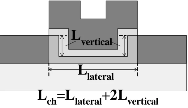
L
lateral
L
vertical
L
ch
=L
lateral
+2L
vertical
-20 -10 0 10 20 30 40 10-14 10-13 10-12 10-11 10-10 10-9 10-8 10-7 10-6 10-5 10-4
Wch/Lch = 10/9.9
(µm/
µm
)No hydrogenation
Vds = 0.1 VDr
ain Cu
rr
ent, (
A
)
Gate Voltage,(V)
Conv. coplanar
D-SAGRSD
Vds = 5 VFig. 2-3 I
ds– V
gstransfer characteristics of the proposed D-SAGRSD TFT and the
(a)
(b)
Fig. 2-4 Simulation current flow lines of (a) the conventional co-planar TFT; (b) the
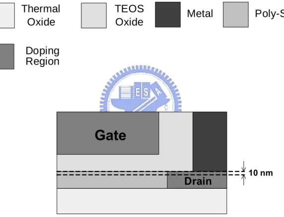
Gate
Drain
10 nmThermal
Oxide
TEOS
Oxide
Metal
Poly-Si
Doping
Region
Fig. 2-5 Simulation position of the lateral electric field of the conventional co-planar
Drain
Thermal
Oxide
TEOS
Oxide
Metal
Poly-Si
Doping
Region
B:
130 nmA:
10 nmC:
10 nmGate
Fig. 2-6 Simulation positions of the lateral electric field of the proposed D-SAGRSD
Table 2-1 Maximum lateral electric field of the conventional and proposed
TFT structures in the ON-state.
0.421
0.108
0.082
0.110
Max. Lateral Electric Field
(MV/cm)
D-SAGRSD
C
D-SAGRSD
B
D-SAGRSD
A
Conventional
co-planar
ON-state
@V
gs
= 30 V; V
ds
= 20 V
0.421
0.108
0.082
0.110
Max. Lateral Electric Field
(MV/cm)
D-SAGRSD
C
D-SAGRSD
B
D-SAGRSD
A
Conventional
co-planar
ON-state
@V
gs
= 30 V; V
ds
= 20 V
10.6 10.8 11.0 11.2 11.4 11.6 11.8 12.0 12.2 12.4 0.0 0.5 1.0 1.5 2.0 2.5 3.0 3.5 4.0 4.5 5.0 Oxide
Gate Thicker Channel Drain
La
te
ra
l El
ec
tr
ic
Fi
eld
(MV
/c
m
)
X-axis distance (
µ
m)
Conv.coplanar
D-SAGRSD
Channel Drain 1.0044 MV/cm 1.1097 MV/cm Vgs = - 10 V; Vds = 5 V; Lch = 10 µmFig. 2-7 Simulated lateral electric field distribution of the proposed D-SAGRSD
TFT and the conventional co-planar TFT in the OFF-state.
Table2-2 Maximum lateral electric field of the conventional and proposed
TFT structures in the OFF-state.
0.338
0.366
1.00
1.11
Max. Lateral Electric Field
(MV/cm)
D-SAGRSD
C
D-SAGRSD
B
D-SAGRSD
A
Conventional
co-planar
OFF-state
@V
gs
= -10 V; V
ds
= 5 V
0.338
0.366
1.00
1.11
Max. Lateral Electric Field
(MV/cm)
D-SAGRSD
C
D-SAGRSD
B
D-SAGRSD
A
Conventional
co-planar
OFF-state
@V
gs
= -10 V; V
ds
= 5 V
0 5 10 15 20 25 0 200 400 600 800 1000 0.0 0.2 0.4 0 2 4 6 8 10 12 Vgs= 30 V D rai n Cu rr en t, ( µ A) Drain Voltage, (V) Conv. coplanar D-SAGRSD Vgs= 35 V
W/L = 10/9.9
(µm/
µm
)No hydrogenation
Vgs= 30 V
Vgs= 35 V
Conv. coplanar
D-SAGRSD
Dr
ain Cu
rre
nt, (
µ
A)
Drain Voltage, (V)
Fig. 2-8 I
ds– V
dsoutput characteristics of the proposed D-SAGRSD TFT and the
conventional co-planar TFT. The insert plots are the I
ds– V
dsoutput
characteristics of the proposed D-SAGRSD TFT and the conventional
Chapter 3
A Novel Four-Mask Step Low-Temperature Polysilicon
Thin-Film Transistors with Self-Aligned Raised Source/Drain
(SARSD)
3.1. I
NTRODUCTIONLow-temperature polycrystalline silicon (LTPS) TFTs appear to be one of the most promising technologies for the ultimate goal of building large area electronic systems on glass substrate [3.1]. In flat panel liquid crystal, electroluminescent, and plasma displays, as well as other applications such as high-speed printers and page width optical scanners, poly-Si TFTs can be used to integrate peripheral driver circuits on glass for system integration [3.2]. In order to integrate peripheral driving circuits on the same glass substrate, both a large current drive and a high drain breakdown voltage are necessary for poly-Si TFT device characteristics. It has been previously reported that the use of a thinner active channel film is beneficial for obtaining a higher current drive [3.3],[3.4].The use of thin active channel layer, however, inevitably results in poor source/drain contact and large parasitic series resistance. An ideal TFT device structure, therefore, should consist of a thin active channel region, while maintaining a thick source/drain region. The thick source/drain region serves on not only to reduce the lateral electric field, thus maintaining the breakdown voltage [3.5],[3.6],
but to reduce the source/drain series resistance. Pervious methods used to fabricate such ideal structures with thin active channel and thick source/drain region, however, are not self-aligned in nature, and require additional masks [3.5],[3.6], when compared to the conventional co-planar TFTs.
In chapter 2, the D-SAGRSD TFT has been proposed. However, this structure has a slightly low ON-state drain current and a low ON/OFF current ratio, even the OFF-state leakage current can be suppressed. In this chapter, a novel TFT with self-aligned raised source/drain (SARSD) structure is proposed. The new device features a thin, wider active channel region and a thick source/drain region. This new device also has a higher ON-state drain current and a higher ON/OFF current ratio than those of the D-SAGRSD TFT. Moreover, the OFF-state leakage current of the SARSD TFT is as low as that of the D-SAGRSD TFT. The RSD regions of this new device are self-aligned and no additional mask is needed.
3.2. D
EVICEF
ABRICATIONThe fabrication processes of the novel n-channel poly-Si SARSD TFT were as follows: A 350-nm thick α-Si layer for active region was deposited by low pressure chemical vapor deposition (LPCVD) system using SiH4 at 550°C on 500-nm thermal oxidized silicon wafers. After patterning, the thin α-Si (50 nm) regions and the thick α-Si (350 nm) regions were formed using reactive ion
etching (RIE) at this mask step, as shown in Fig. 3-1(a). The widths of the thick α-Si (350 nm) regions were 5 µm. Then the deposited α-Si film was annealed in nitrogen ambient at 600°C for 24 h to become the poly-Si film. After recrystallization, the etching damages of the channel surface were recovered and the surface roughness is approximately 3 nm. A 50-nm plasma enhanced chemical vapor deposition (PECVD) gate oxide layer was deposited at 350 °C, and then a 300-nm LPCVD poly-Si gate was deposited. After defined the undoped gate region (gate mask area = Lch
x
Wch, as shown in Fig. 3-2), the remnant 50-nm oxide film and 50-nm poly-Si film would be further removed using the RIE system to form an isolated active region, as shown in Figs. 3-1(b) and 3-1(c). After the photoresist was removed, Gate, Source and Drain regions were formed by ion implantation of Phosphorous (Dose = 5 x 1015 cm-2 at 50 keV) and then activated in nitrogen ambient at 600 °C for 24 h, as shown in Fig. 3-1(c). It is worth pointing out that the gate region width (Wch) is larger than that of the source/drain region (Wsd). Therefore, a thin and wider active region would be formed below the whole of gate region, as shown in Fig. 3-2. After the source, drain and gate activation, the 500-nm passivation oxide was deposited by PECVD. Contact holes were opened using wet etching of the passivation oxide layer. A layer of aluminum was then deposited by thermal coater system with a thickness of 600 nm. After metal patterning, a forming gas anneal is performed at 400°C for 30 min. The total masks of our fabrication processes are four masks, which are less than those of conventional processes in a RSD poly-Si TFT [3.5],[3.6]. For comparison, the conventional co-planar poly-Si TFTs with 50-nm channel thickness were also
fabricated in the same run.
3.3
R
ESULTS ANDD
ISCUSSIONFig. 3-3 shows SEM photograph of the proposed SARSD TFT structure. To ensure that current flow of the proposed SARSD structure would be as shown in Fig. 3-2, the 2-D numerical simulator MEDICI was used. Fig. 3-4 shows the simulated current flow lines of the conventional co-planar and proposed SARSD poly-Si TFT structures in ON-state. The channel length and width of the simulated conventional co-planar structure are 15 µm and 5 µm, respectively. From the simulation results in Fig. 3-4(a), the simulated current flow lines of the conventional structure are uniform distribution in the channel region and source/drain regions. However, for the proposed SARSD structure as shown in Fig. 3-4(b), the current flow paths are different from the conventional sample in ON-state. It is because that the channel width is wider than source/drain width, and wide channel width would obtain a high drain current. Therefore, it can be convinced that the proposed RSD structure would obtain a higher drain current than that of conventional co-planar one.
As shown in Fig. 3-5, the proposed SARSD TFT has a higher ON-state current (Vgs = 30V) and a lower OFF-state leakage current (Vgs = -15V) than those of the conventional TFT. In ON-state, the main reasons of high ON-state current are due to wide channel width (Wch = 33 µm) and small source/drain parasitic resistances [3.6]. On the contrary, in OFF-state, the minimum
OFF-state leakage current of the proposed SARSD TFT is only slightly larger than that of the conventional TFT. It is because that the leakage current is determined by the electron-hole pair generation rate in the depletion region at the drain edge. The pair generation rate is strongly dependent on the number of trap-states in the forbidden gap, lateral electric field and a generation volume of the depletion region [3.7]-[3.9]. Although a thick drain region causes the generation volume of the SARSD TFT (must be approximately Wsd
x thickness of the depletion region) to
increase, the maximum lateral electric field near the drain region of the proposed SARSD TFT is largely dropped from 2.13 MV/cm to 1.57 MV/cm due to thick source/drain region [3.10]. At high drain and reverse gate bias (Vds = 5 V, Vgs = -15 V), the leakage current would be due to the thermionic field emission via grain boundary defects [3.11]. Therefore, the proposed SARSD TFT has a lower OFF-state leakage current than that of the conventional TFT because the maximum lateral electric field near the drain region is largely dropped, even though the generation volume would be increased. As shown in Fig. 3-6, the proposed SARSD TFT has a higher saturation current and a lower parasitic resistance than those of the conventional one for different gate bias.Fig. 3-7 shows the Ids - Vgs transfer characteristics of the proposed SARSD TFT with different channel width. Fig. 3-8 shows maximum ON-state current and minimum OFF-state leakage current of the proposed SARSD TFT with various the side channel width, and the conventional co-planar TFT. It is obvious that the ON-state current is increased with increasing the channel width. However, as shown in Fig. 3-8, the minimum OFF-state leakage current is also
increased with increasing the channel width. Fig. 3-9 shows the OFF-state leakage current of the proposed SARSD TFT with various the side channel width, and the conventional co-planar TFT measured at Vgs = -15 V and Vds = 5 V. In Fig. 3-9, it is obvious that the OFF-state leakage current of the proposed SARSD TFT is significant lower than that of the conventional co-planar TFT for different channel width. Moreover, as shown in Fig. 3-10, the optimum condition of the SARSD TFT for the case of Lch /Wsd = 15 µm/ 5 µm is Wsc = 2 µm.
3.4. S
UMMARYIn this chapter, a novel four mask steps n-channel low-temperature poly-Si TFT with a self-aligned raised source/drain region and a thin channel was proposed and investigated. The gate mask was used to form a large area thin-channel region below the gate region, and the self-aligned raised source/drain region can be formed without the additional mask step. A lower off-sate leakage current and a higher ON/OFF current ratio can be obtained for the proposed SARSD TFT. The TFT fabrication processes are fully compatible with the conventional four-mask ones. This new TFT structure may be an attractive device structure for future high-performance large-area device applications.
References
[3.1] Anish. Kumar K.P. and Johnny K. O. Sin, “Influence of lateral electric field on the anomalous leakage current in polysilicon TFT,” IEEE Electron Device Letters, vol. 20, no. 1, pp. 27-29, Jan. 1999.
[3.2] M G Clark, “Current status and future prospects of poly-Si devices,” IEE Proc.-Circuits Devices Syst, vol. 141, no. 1, pp. 3-8, Feb. 1999.
[3.3] Takashi Noguchi, Hisao Hayashi, and Takefumi Ohshima, “Low Temperature Polysilicon Super-Thin-Film Transistor(LSFT),” Jpn. J. Appl. Phys., vol. 25, no. 2, pp. L121-L123, Feb. 1986.
[3.4] Mitsutoshi Miyasaka, Takahiro Komatsu, W. Itoh, A. Yamaguchi, and H. Ohashima, “Effects of channel thickness on poly-crystalline silicon thin film transistor,” Ext. Abstr. SSDM, pp. 647-650, 1995.
[3.5] Makoto Yoshimi, Minoru Takahashi, Tetsunori Wada, Kouichi Kato, Shigeru Kambayashi, Masato Kemmochi, and Kenji Natori, “Analysis of the drain breakdown mechanism in ultra-thin-film SOI MOSFETs,” IEEE Trans. Electron Devices, vol. 37, no. 9, pp. 2015-2021, Sept. 1990.
[3.6] Shengdong Zhang, Chunxiang Zhu, Johnny K. O. Sin, and Philip K. T. Mok, “A Novel Ultrathin Elevated Channel Low-temperature Poly-Si TFT,” IEEE Electron Device Letters, vol. 20, no. 11, pp. 569-571, Nov. 1999.
[3.7] O. K. B. Lui, M. J. Quinn, S. W-B. Tam, T. M. Brown, P. Migliorato and H. Ohshima, “Investigation of the Low Field Leakage Current Mechanism in Polysilicon TFT’s,” IEEE Trans. Electron Devices, vol. 45, no. 1, pp. 213-217, Jan. 1998.
[3.8] O. K. B. Lui and P. Migliorato, “A new generation recombination model for device simulation including the Poole-Frenkle effect and phonon-assisted tunneling,” Solid-State Electronics, vol. 41, no. 4, pp. 575-583, 1997.
[3.9] S. D. Brotherton, J. R. Ayres and M. J. Trainor, “Control and analysis of leakage currents in poly-Si thin-film transistors,” J. Appl. Phys., vol. 79, issue 2, pp. 895-904, Jan. 1996. [3.10] Anish. Kumar K.P., Johnny K. O. Sin, Cuong T. Nguyen, and Ping K. Ko, “Kink-Free
Polycrystalline Silicon Double-Gate Elevated Channel Thin-Film Transistors,” IEEE Trans. Electron Devices, vol. 45, no. 12, pp. 2514-2520, Dec. 1998.
[3.11] Chul Ha Kim, and Ki-Soo Sohn, “Temperature dependent leakage currents in polycrystalline silicon thin film transistors,” J. Appl. Phys., vol. 81, no. 12, pp. 8084-8090, June. 1997.
Ion Imp.
(c)
Thermal Oxide
G
S
50 nmD
350 nm 300 nmThermal Oxide
R. I. E.
(b)
50 nm 300 nm 50 nm 50 nmThermal Oxide
(a)
350 nm 50 nmP. R. Poly-Si Gate Oxide Doping Region
Thicker Channel Region
Fig. 3-1 (a)-(c) Schematic cross section of the major fabrication steps of the
L
ch
D
W
sd
W
ch
I
main
I
add
I
add
I
ds
= I
main
+ I
add
S
W
sc
W
sc
Poly-Si
Doping Region
Thicker Channel
Region
Fig. 3-2 Schematic diagram of the current flow lines of the proposed SARSD
DRAIN
GATE
SOURCE
Fig. 3-4 Current flow lines simulated by MEDICI in (a) the conventional co-planar
structure with L
ch= 15 µm and W
ch= W
sd= 5 µm; (b) the SARSD
-20 -10 0 10 20 30 10-12 10-11 10-10 10-9 10-8 10-7 10-6 10-5 10-4 Lch = 15 µm; Wsd = 5 µm @ Vds = 5 V No hydrogenation Drain C u rrent ( A ) Gate Vlotage (V) Prop. SARSD (F) Prop. SARSD (R) Conv. co-planar
Fig. 3-5 I
ds-V
gstransfer characteristics of the proposed SARSD TFT in both forward
mode (F) and reverse mode (R) and the conventional co-planar TFT, in
0 10 20 30 40 0 20 40 60 80 100 120 140 160 180 200 Vgs= 15 V Lch = 15 µm; Wsd = 5 µm No hydrogenation Dr ain Cur re n t ( µ A) Drain Voltage (V) Conv. co-planar Prop. SARSD Vgs= 20 V
Fig. 3-6 I
ds-V
dsoutput characteristics of the proposed SARSD TFT and the
-20 -10 0 10 20 30 10-12 10-11 10-10 10-9 10-8 10-7 10-6 10-5 10-4 Lch = 15 µm; Wsd = 5 µm @ Vds = 5 V No hydrogenation
Gate Voltage (V)
Drain Current
(
A
)
W ch= 5 µm 9 µm 13 µm 17 µm 25 µm 33 µm SARSD TFTFig. 3-7 I
ds-V
gstransfer characteristics of the proposed SARSD TFT with different
-6 -4 -2 0 2 4 6 8 10 12 14 16 18 0.1 1 10 100 1000 Wsd = 5 µm; Lch = 15 µm @ Vds = 5 V
Wsc=(( Wch- Wsd)/2), (
µm)
Maxi mu m ON-state cu rr ent ( µ A ), measu re d at V gs = 30 V conv. co-planar TFT SARSD TFT 0.1 1 10 100 1000 Mi n imum OF F -state l eakag e cu rr en t ( pA )Fig. 3-8 Maximum ON-state current and minimum OFF-state leakage current of the
proposed SARSD TFT with various the side channel width, and the
-6 -4 -2 0 2 4 6 8 10 12 14 16 18 10-8 10-7 10-6 Wsd = 5 µm; Lch = 15 µm @ Vds = 5 V OFF -state leak ag e cu rrent ( µ A ), me asured at V gs = -15 V Wsc=(( Wch- Wsd)/2), (µm) SARSD TFT conv. co-planar TFT
Fig. 3-9 OFF-state leakage current of the proposed SARSD TFT with various the
side channel width, and the conventional co-planar TFT measured at
-6 -4 -2 0 2 4 6 8 10 12 14 16 18 0.75 1.00 1.25 1.50 1.75 2.00 2.25 SARSD TFT Wsd = 5 µm; Lch = 15 µm @ Vds = 5 V conv. co-planar TFT
Wsc=(( Wch- Wsd)/2), (
µm)
O N /O FF Ra ti o ( x1 07 ) Optimum condition (Wsc= 2)Fig. 3-10 ON/OFF current ratio of the proposed SARSD TFT with various the
Chapter 4
Effect of Channel Width Widening on a Poly-Si Thin-Film
Transistor Structure in the Linear Region
4.1 I
NTRODUCTIONLow-temperature polycrystalline silicon thin-film transistors (LTPS TFTs) are one of the most promising technologies for the ultimate goal of building large area electronic systems on glass substrates [4.1]. In flat panel liquid crystal, electroluminescence, and plasma displays, as well as other applications such as high-speed printers and page-width optical scanners, Poly-Si TFTs can be utilized to integrate peripheral driver circuits on glass for system integration [4.2]. To integrate peripheral driving circuits on the same glass substrate, a large current drive and a high drain breakdown voltage are necessary for poly-Si TFT devices. Previous studies reported that use of a thin active channel film is beneficial for obtaining a high current drive [4.3],[4.4]. However, use of a thin active channel layer typically results in poor source/drain contact and large parasitic series resistance. A thick source/drain region not only reduces the lateral electric field, thus maintaining the breakdown voltage [4.5],[4.6], it also reduces the source/drain series resistance [4.6]. Therefore, an ideal TFT device structure should consist of a thin active channel region while maintaining a thick source/drain region.