J. Electrochem. Soc., Vol. 140, No. 9, September 1993 9 The Electrochemical Society, Inc.
2645
P b - r u t h e n a t e i n t e r l a y e r due to intermixing at high temper-atures reduces the compositional g r a d i e n t between the electrode and the ferroelectric and thereby the tendency for defect migration is less. In effect, RuO~ electrodes in PZT thin film capacitors reduce the tendency for defect m i g r a - tion and e n t r a p m e n t at the interface t h a t m a y result in structural damage to the interface and eventual loss of po- larization.
H i g h e r dc leakage current levels were observed in PZT films on P t electrodes when compared to RuO2 electrodes. Films on RuO~ electrodes also showed b e t t e r TDDB c h a r a c - teristics under an ac field. Improvement in d e g r a d a t i o n properties were observed w i t h decreasing thickness of the films. The reason for this observation is a t t r i b u t e d to the b e t t e r adhesion of the thinner films on the b o t t o m electrode.
Acknowledgment
This w o r k was supported in p a r t b y DARPA through a project from ONR. This w o r k was supported also by Center for A d v a n c e d Ceramic Materials, The Virginia Center for Innovative Technology. The authors t h a n k Dr. I. K. Yoo, Dr. C. K. Kwok, Dr. N. R. Parikh, and Mr. E. A. Hill for their useful contributions.
Manuscript s u b m i t t e d Jan. 6, 1993; revised m a n u s c r i p t received A p r i l 1, 1993.
The Virginia Polytechnic Institute and State University
assisted in meeting the publication costs of this article.
REFERENCES
1. D. W. Chapman,
J. Appl. Phys., 40, 2381 (1969).
2. R. B. Atkin, Ferroelectrics, 3, 213 (1972).3. T. N a k a g a w a , J. Yamaguchi, T. Usuki, Y. Matsui, M. Okuyama, and Y. H a m a k a w a , Jpn, J. Appl. Phys., 18, 897 (1979).
4. M. Sayer, Proceedings of the Sixth Symposium on Ap-
p
lied Ferroelectricity,
p. 559,IEEE,
New York1986).
5. J. T. Evance and R. Wormack, IEEE J. Solid State Cir-
cuits,
23, 1171 (1988).6. J. E Scott and C. A. Paz De Araujo, Science, 246, 1400 (1989}.
7. A. Tasch and L. Parker, Proc.
IEEE,
77, 374 (1989). 8. D. B. F r a s e r and J. R. Maldonado,J. Appl. Phys.,
41,2172 (1970).
9. I. S. Zheludev, Physics of Crystalline Dielectrics, Elec-
trical Properties,
Vol. 2, p. 474, Plenum, New York(1971).
10. A. Y. Kudzin, T. U. Panchenko, and S. P. Yudin,
Sov.
Phys. Solid State,
16, 1589 (1975).11. G. Rohrer, S. Narayan, L. McMillan, and A. Kulkarni,
J. Vac. Sci. Technol.
A, 6, 1756 (1988).12. H. M. Duiker, E D. Beale, and J. F. Scott,
Bull. Am.
Phys. Soc.,
33, 539 (1988).13. I. K. Yoo and S. B. Desu,
Mater. Sci. Eng.,
B13, 319 (1992).14. N. R. Parikh, J. T. Stephen, M. L. Swanson, and E. A. Myers, Mat. Res. Soc. Symp. Proc., 200, 193 (1990). 15. L. K r u s i n - E l b a u m and M. Whittmer, This Journal, 13~,
2610 (1988).
16. M. L. Green, M. E. Gross, L. E. Kappa, K. J. Schnoes, and D. Barsen,
ibid.,
132, 2677 (1985).17. S. Saito and K. Kuramasu, Jpn. J. Appl. Phys., 31, 135 (1992).
18. G. Yi and M. Sayer,
Ceram. Bull.,
70, 1173 (1991). 19. R. D. Standley and U. Ramaswamy, J. Appl. Phys., 46,4887 (1975).
20. S.B. Desu and C. K. Kwok, Mat. Res. Soc. Symp. Proc., 200, 267 (1990).
21. J. M. Longo, E M. Raccah and J. B. Goodenough,
Mat.
Res. Bull.,
4, 191 (1969).22. Anonymous,
Microprocessors and Microsystems,
13, 291 (1989).23. J. E Scott~ C. A. Araujo, B. M. Melnick, L. D. McMillan, and R. Zuleeg, J. Appl. Phys., 70, 383 (1991).
Characterization of Semi-Insulating Polycrystalline Silicon
Prepared by Low Pressure Chemical Vapor Deposition
Tien Sheng Chao
National Nano Devices Laboratory, Hsinchu 300, Taiwan, China
Chung Len Lee* and Tan Fu Lei
Department of Electronics Engineering and Institute of Electronics, National Chiao Tung University, Taiwan, China
ABSTRACT
We employed the multiple angle incident ellipsometer to study the growth mechanism and optical properties of semi-insulating polycrystalline silicon (SIPOS) films deposited b y the low-pressure chemical vapor deposition (LPCVD) technique. A significant difference of the i m a g i n a r y p a r t of the refractive index between film at the edge and those in the central region of the wafer was observed. Our analyses showed t h a t it was consistent with the N20 depletion model. This N20 depletion phenomenon was confirmed b y Auger analysis. Moreover, we found t h a t spatial N20 depletion at the edge of the wafer was greatly influenced b y the flow rate of Sill4 to N20 gases. Excessively high N20 flow r a t e suppressed the silicon microcrystal formation, resulting in a t h i n n e r SIPOS film.
Semi-insulating polycrystalline silicon (SIPOS) has been used as a passivation m a t e r i a l to replace oxide in high voltage semiconductor devicesJ -3 This replacement is be- cause oxide films fail to overcome three challenging p r o b - lems to meet the requirements of modern i n t e g r a t e d - c i r c u i t p l a n a r technology; (i) the existence of fixed charges, usu- ally positive ions, in oxide films. These fixed charges in- duce and accumulate electrons n e a r the silicon/oxide inter- face, which makes it difficult to produce a high voltage p l a n a r transistor; 4 (it) oxide films are not able to keep the
* Electrochemical Society Active Member.
accumulated electron charges or ionic contaminations, such as sodium, from the passivation layer; 5'6 (iii) the hot carrier, once injected into oxide, stays long in it resulting in a w a l k - o u t phenomenon of b r e a k d o w n voltage in the p - n junction. These three problems l e a d to charges t r a p p e d in oxide films and subsequent inducement of charges 7 of op- posite p o l a r i t y n e a r the surface. Therefore, the stability and r e l i a b i l i t y of the circuit passivation b y oxide films are not achievable in high voltage semiconductor devices.
In contrast to oxide, SIPOS films are semi-insulating and almost n e u t r a l for its deep level centers pinning the F e r m i - level n e a r midgap. 8'9 Therefore, SIPOS can be used for sur-
) unless CC License in place (see abstract).
ecsdl.org/site/terms_use
address. Redistribution subject to ECS terms of use (see
140.113.38.11
2646
J. Electrochem. Soc.,
Vol. 140, No. 9, September 1993 9 The Electrochemical Society, Inc.face passivation on both p- a n d n-type silicon. When a sili- con surface is passivated by SIPOS, the contaminating ions drift into the passivation layer. Momentarily, the induced opposite polarity charges either neutralize the charges or form a space-charge region w i t h i n the SIPOS layer. Conse- quently, a shielding effect in the silicon surface region is achieved, a n d this copes with the problem of the injected hot carrier at high fields.
SIPOS film usually has been deposited by low-pressure chemical vapor deposition (LPCVD) technique using mix- ture of silane (Sill4) a n d nitrous oxide (NfO) at 650~ TM This
material has been reported as an excellent passivation film for high voltage transistors 1'2'n a n d carrier injector in elec- trically erasable a n d programmable read-only memories (EEPROMs). TM It, instead of polysilicon, was used also as an
emitter because of its larger b a n d gap, which offers better minority carrier blocking properties t h a n that of the con- ventional diffused emitter33 The chemical composition of SIPOS is SiO=, where x ranges from 0.48 to less t h a n 2, a n d the oxygen concentration increased with the partial pres- sure of N20. From the results of transmission electron mi- croscopic (TEM) analysis, Hamasaki et al.3 found that the SIPOS consisted of silicon microcrystals, silicon oxide, a n d disordered silicon. The size of silicon microcrystals i n SIPOS decreased as the oxygen concentration increased,
i.e., increasing the partial pressure of N20.
Multiple angle incident (MAI) ellipsometry measure- ment, for its high sensitivity and nondestructiveness, has been used in m a n y fields. It has been applied to character- ize the optical coating, 14 the oxygen-ion-implanted silicon- on-insulator (SOI), 15 multiple-layer heterostructure. ~6 MAI ellipsometry is used here to study the growth mechanism and optical properties of SIPOS. The Auger analysis was employed to characterize the oxygen concentration in the SIPOS film.
Experimental
Silicon wafers, n-type (100), 4-5 ~-cm, were used a n d cleaned by the RCA process. Wafers then were dipped in buffered HF solution followed by a DI water rinse. Subse- quently, a SiO3 film of 220A thickness was grown on those wafers in a dry oxygen a m b i e n t at 1000~ for 17 min. The samples then were p u t into an LPCVD system to deposit SIPOS films. Different flow rate ratios of Sill4 (45 sccm) to N20 (10, 15, 20, 30, and 35 sccm) were used to deposit the SIPOS film at 650~ for 30 min. Samples were measured by MAI ellipsometry with the incident angles varying between 65 and 72 degrees at the wavelength of 632.8 nm. A sum of the least squares error fitting method was used to fit the optical constant ( N = N - i K ) a n d thickness (T) of SIPOS, where N and K are the real and the imaginary part of the refractiv e index N of SIPOS, respectively. I n the fitting pro- cess, a reasonable range of values of N, K, a n d T is given. Then, the simulated values of (h, @) can be calculated for a corresponding set of (N, K, T). The sum of the error of the best fit case between the measured and the simulated ellip- sometric angle h a n d @ was always less t h a n 1 degree in our measurements.
Results and Discussion
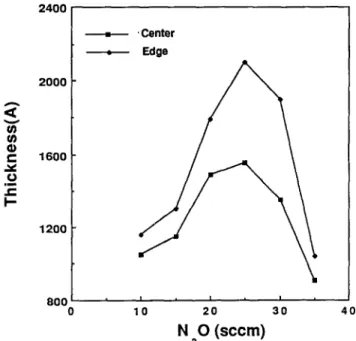
Figure 1 s h o w s the thickness of S I P O S films deposited w i t h different m i x i n g flow rates of Sill4 a n d N f O . T h e flow rate of Sill4 w a s fixed at 45 s c c m while the flow rate of N f O w a s varied b e t w e e n i0 a n d 35 sccm. A s seen in Fig. i, the thickness of S I P O S increases rapidly w i t h N f O flow rate a n d then decreases m o n o t o n o u s l y as the N f O flow rate ex- ceeds 25 sccm. Initially, as the N f O flow w a s varied, the partial pressure of N f O at the surface increased corre- spondingly, w h i c h resulted in a n increase of S I P O S film thickness. H o w e v e r , as the flow rate of N 2 0 e x c e e d e d 25 sccm, the w a f e r surface is m o s t l y saturated w i t h NfO. This N f O saturation suppressed surface reaction o n Si sur- face a n d further nucleation of Si microcrystal. Similar sur- face reactions w e r e observed for the S i H J O 2 system. ~7 A t high o x y g e n concentration, the surface w a s m e r e l y satu- rated w i t h a b s o r b e d o x y g e n a n d further deposition reac- tion w i t h silane w e r e blocked. Therefore, w e conclude that
the silane-oxygen reaction is dominated by gas species near the wafer surface. We also note in Fig. 1 that the SIPOS film thickness at the edge of the wafer (3 cm from the center of a 3 in. wafer) is thicker t h a n that i n the center. This deple- tion effect, TM which resulted from preferential reactant gas
concentration also has been observed for m a n y conven- tional end-feed LPCVD systems. Deposition rates were greater on wafers near the inlet of gas t h a n the center of the wafer. As a result, the thickness of SIPOS films at the edge of the wafer was thicker t h a n that at the center. The top view of the wafer deposited at a N20 flow rate of 20, 25, a n d 30 sccm were examined also. Circular rings of various col- ors were evident, indicating a thickness variation across the wafer. As seen in Fig. 1, the thickness difference be- tween the edge a n d the central region is m i n i m a l for N20 flow rate of either 10 or 35 sccm. Correspondingly, colorful rings were not observed on wafers with SIPOS film de- posited u n d e r these conditions.
Figure 2 shows the measured real part, N, of the refrac- tive index of SIPOS as a function of the N20 flow rate. For N20 flow rate less t h a n 20 sccm, the N of the wafer center region is slightly larger t h a n that of the edge. As the flow rate of N20 exceeds 20 sccm, the N v a l u e of the edge and the center reaches a same value. Figure 3 shows the measured imaginary part, K, of the refractive index of SIPOS v s . the N20 flow rate. The K value decreases steadily with increas- ing N20 flow rate. This decrease indicates that the absorp- tion properties of the SIPOS films decreased with increase of the oxygen concentration. For a wavelength of 632.8 rim, the silicon dioxide is almost transparent, and, hence, K is zero. The absorption of the amorphous silicon is larger t h a n single-crystalline silicon. As reported previously, 3 SIPOS films consist of Si microcrystal, disordered St, a n d Si oxide. Therefore, as the oxygen concentration in the SIPOS film increases, the adsorption of the SIPOS decreases. In Fig. 3, it is clearly evident that the adsorption coefficient K of the edge region is lower t h a n that of center. This result is be- cause the N20 gas was consumed more at the edge t h a n in the center, resulting in a higher oxygen concentration at the edge. This result is consistent with the depletion effect ob- served in Fig. 1.
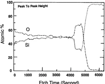
To further confirm the model of the N~O depletion in SIPOS film deposition, some samples were characterized by Auger analyses. A 1000~ thick thermal oxide film was analyzed and used as a standard. Figures 4 and 5 show the atomic ratio % of SIPOS film at the edge a n d the center of
,<
v u) (n 4) t- o e- l - 2400 2000 1600 1200 800 9 ' Center = Edge 10 20 30N 0
(sccm)
2 40Fig. 1. The measured thickness (A) of SIPOS deposited in on LPCVD system at 650~ for 30 min. The flow rate of Sill4 is 45 sccm and the mixing N20 flow rate is 10 to 35 sccm. The thickness of the edge is measured at a point 3 cm from center region.
) unless CC License in place (see abstract).
ecsdl.org/site/terms_use
address. Redistribution subject to ECS terms of use (see
140.113.38.11
2647 3.25 3.00 9 Center
Z
2.75 ~ J...
2.50 o m 4 - ) ~ J 2.25 2.00 1.75J. Electrochem. Soc.,
Vol. 140, No. 9, S e p t e m b e r 1993 9 The Electrochemical Society, Inc.I , I , I , 10 20 30
N=O ( s c c m )
40 o o100 j Peak To Peak Height ." ...
o. 80~- :i
o
60 I':""~'--~ . - ! ! .: ...si
\ :i
I'
I. 2O ~. t \ o , I , I , I ,I'\--.
0 1000 2000 3000 4000Etch Time (Second)
Fig. 4. Auger analysis of the atomic ratio of Si and O of the SIPOS film (Sill4 : N20 = 45 : 25 sccm) at the edge of the wafer.
Fig. 2. The measured real port of the refractive index of SIPOS by
MAI ellipsometry for 45 sccm Sill4 and for different N20 flow rates changing from 10 to 35 sccm. The edge point is measured from the center at a distance of 3 cm.
100
80
. ~ . . . ~
Peak To Peak Height .-"
a wafer, respectively. These films w e r e d e p o s i t e d w i t h 45 ~ o s c c m SiH~ a n d 25 s c c m N20. The o x y g e n c o n c e n t r a t i o n at .o 60 t h e e d g e of t h e w a f e r is l a r g e r t h a n t h a t of t h e center, espe- E cially n e a r t h e s a m p l e surface. This c o n f i r m e d o u r N20 de- o p l e t i o n m o d e l as m e n t i o n e d above. F i g u r e 6 shows t h e ~" 40 a t o m i c r a t i o % of Si a n d O of a d i f f e r e n t s a m p l e d e p o s i t e d
w i t h N20 f l o w r a t e of 15 sccm a n d a f i x e d Sill4 f l o w r a t e of
45 sccm. T h e o x y g e n c o n c e n t r a t i o n is o n l y 30% a n d is u n i - 2 0
f o r m across t h e e n t i r e film. F r o m t h e results of A u g e r a n a l - ysis a n d t h e e l l i p s o m e t r y m e a s u r e m e n t , w e c o n c l u d e t h a t a u n i f o r m t h i c k n e s s S I P O S f i l m is a c h i e v a b l e w i t h N20 f l o w 0 r a t e less t h a n 15 sccm. A s l o w e r f l o w r a t e of N20 also w o u l d r e s u l t in a u n i f o r m S I P O S f i l m w i t h a c o n s t a n t S i / O ratio.
Conclusion
In this w o r k , t h e MAI e l l i p s o m e t e r w a s u s e d to s t u d y t h e g r o w t h m e c h a n i s m a n d o p t i c a l p r o p e r t i e s of t h e S I P O S films g r o w n b y an L P C V D t e c h n i q u e . F o r a N20 f l o w r a t e, o
:
I-
.~..~7;.
...
.-.:::.~.<>-,~-v::.
~~ "'"'~
~l
Si
:~
... 9 ...: ~ t,
I
,
I
, I, ... 4 -
1000
2000
3000
4000
sooo
6000
Etch Time (Second)
Fig. 5. Auger analysis of the atomic ratio of Si and O of the SIPOS
film (Sill4 : N20 = 45 : 25 sccm) at the center of the wafer.
fl} "0 e- > 0 x - - q . . 1 . 0 0 . 8 0 . 6 0 . 4 0 . 2 0.0 0 4 0 9 Center . Edge = lO 2 0 30
N=O ( s c c m )
Fig. 3. The measured imaginary port of the refradive index of SIPOS by MAI ellipsomeh'y for 45 sccm Sill4 and for different N20 flow rates changing from 10 to 35 sccm. The edge point is measured
from the center at a distance of 3 cm.
less t h a n 25 sccm, t h e t h i c k n e s s of t h e S I P O S f i l m i n c r e a s e d w i t h N20 f l o w rate. As N20 f l o w r a t e w a s r a i s e d b e y o n d 25 sccm, t h e e x i s t e n c e of e x c e s s i v e N20 n e a r t h e w a f e r sur- face, w h i c h s u p p r e s s e d t h e s u r f a c e r e a c t i o n f o r silicon m i - 100 80 o 60
E
o~.
4o
2 0Peak To Peak Height
Si
%. O
0 , I , I , I ,
0 1000 2000 3000 4000 5000 6000 7000
Etch Time (Second)
Fig. 6. Auger analysis of the atomic ratio of Si and O of the SIPOS
film (Sill4 : N20 = 45 : 15 sccm) at the center of the wafer.
) unless CC License in place (see abstract).
ecsdl.org/site/terms_use
address. Redistribution subject to ECS terms of use (see
140.113.38.11
2648
J. Electrochem. Soc.,
Vol. 140, No. 9, September 1993 9 The Electrochemical Society, Inc.crocrystal formation. T h e N 2 0 depletion effect b e c a m e greater for N 2 0 flow rates in the range of 20 to 30 secm. This depletion effect w a s confirmed b y both A u g e r analyses a n d the ellipsometry m e a s u r e m e n t . W e observed that lower flow rates resulted in a S I P O S film of better thickness uni- formity a n d m o r e constant Si/O ratio.
Acknowledgment
This work is supported by the National Science Council of the Republic of China through Contract No. NSC81- 4040-E009-138. The authors t h a n k Dr. P. J. Wang for his helpful discussions.
Manuscript submitted Nov. 4, 1992; revised manuscript received May 12, 1993.
The National Nano Devices Laboratory assisted in meet- ing the publication costs of this article.
RREFERENCES
1. M. Okayama a n d Y. Kawana, IEEE Trans. Electron Devices, ED-23, 826 (1976).
2. A. Mimura, M. Oohayashi, S. Murakami, a n d N. Momma, IEEE Electron Device Lett., EDL-6,189 (1985).
3. M. Hamasaki, T. Adachi, S. Wakayama, a n d M. Kikuchi, J. Appl. Phys., 49, 3987 (1978).
4. B. E. Deal, IEEE Trans. Electron Devices, ED-27, 606 (1980).
5. D. R. Kerr, J. S. Logan, P. J. Burkhardt, and W. A. Pliskin, IBM J. Res. Dev., 8, 376 (1964).
6. E. H. Nicollian a n d J. R. Breuws, MOS Physics and Technology, Wiley, New York (1982).
7. C. A. Neugebauer, Appl. Phys. Lett., 19, 287 (1971). 8. T. Aoki, T. Matsushita, H. Yamoto, H. Hayashi, M.
Okuyuma, and Y. Kawana, Abstract 148, p. 352, The Electrochemical Society Extended Abstracts, Vol. 75-1; Toronto, ON, Canada, May 11-16, 1975. 9. T. Matsushita, in Seventh Conference Solid State
Devices Digest Technical Papers, p. 9, Tokyo (1975). 10. W. R. Knolle a n d H. R. Maxwell, This Journal, 127,
2254 (1980).
11. H. Hayashi, T. Mamine, and T. Matsushita, IEEE Trans. Electron Devices, ED-28, 246 (1981).
12. P. Pan, L. A. Nesbit, R. W. Douse, and R. T. Gleason,
This Journal, 132, 2013 (1985).
13. Y. H. Kwark a n d R. M. Swanson, Solid-State Electron.,
3@, 1121 (1987).
14. K. Memarzadeh, J. Appl. Phys., 64, 3407 (1988). 15. P. Dutta, ibid., 64, 2754 (1988).
16. P. G. Snyder, M. C. Rost, H. Bu-Abbud, and J. A. Wool- lam, ibid., 60, 3293 (1986).
17. C. Cobianu and C. Pavelescu, Thin Solid Films, 117, 211 (1984).
18. S. Wolf and R. N. Tauber, Silicon Processing for the VLSI Era, Vol. 1, 170,' Lattice Press, California (1986).
Improving Metal Oxide Semiconductor Device Performance
Through the Use of Ion Exchange-Purified HF
Vikram Doshi and Lindsey Hall
Texas Instruments, Dallas, Texas 75265
Thomas Wear
SEMATECH, Austin, Texas 78741
John Davison*
Athens Corporation, Oceanside, California 92056
ABSTRACT
I o n - e x c h a n g e purification systems w e r e e m p l o y e d at t w o different semiconductor metal oxide semiconductor ( M O S ) w a f e r fabs to purify the dilute hydrofluoric acid solutions used in cleaning silicon wafers. O n e lab p e r f o r m e d the H F cleans in i m m e r s i o n baths while the other lab used a spray cleaner. B o t h labs observed i m p r o v e m e n t s in device performance, as m e a s u r e d in split-lot gate oxide integrity tests, after they b e g a n using the ion exchange-purified H E O n e lab also observed a significant i m p r o v e m e n t in refresh characterization time, a n d a 5 % yield i m p r o v e m e n t at multiprobe. These i m p r o v e - m e n t s are believed d u e to the lower levels of metallic impurities in the ion exchange-purified HF. Impurity levels of over 30 elements in the treated H F are routinely b e l o w 1 ppb.
In 1989, the first hydrofluoric acid reprocessor, or HFR, was tested successfully at Texas Instruments 1 Mbit DRAM lab, DMOS IV, in Dallas, Texas. I The HFR used filters and ion exchangers to remove particulate a n d ionic impurities from dilute HE The first HFR was designed ~o recycle and repurify the HF solutions used to clean furnace tubes and other quartz parts. Analysis of the reprocessed acid soon indicated that ion exchange technology had the ability to product ultrapure HF solutions. 2
About the same time the first HFR began reprocessing the used quartz-cleaning HF in DMOS IV, the lab experi- enced severe problems in the wafer cleaning process. The problems were related to the purity of the dilute HF. These problems were corrected by switching to high purity HF from Japan, a n d implementing some process modifications. Importing HF was expensive, so, in late 1990, another HFR
* Electrochemical Society Active Member.
was installed by TI's Chemical Operations Department to manufacture high purity dilute HF solutions at low cost. The HFR proved capable of making high purity HF solu- tions reliably and consistently. The next step was to qualify the HF for use in the wet-clean process. The qualification took place in DMOS IV since they had a demonstrated need for high purity dilute HE The ion exchange (IE) purified HF from the HFR was compared directly to the high purity HF from J a p a n then in use in a series of split-lot tests car- ried out simultaneously in identical wet-process hoods. No changes to the equipment, and only minor changes to the chemical distribution systems, were required. Thus, the only variable in the tests was the HE The results of these tests indicate with a high degree of certainty that the IE purified HF gives cleaner wafer surfaces, fewer defects, and higher yields.
Also in late 1990, an HFR was installed at SEMATECH in Austin, Texas. For some time after its initial qualification, 3
) unless CC License in place (see abstract).
ecsdl.org/site/terms_use
address. Redistribution subject to ECS terms of use (see
140.113.38.11