ELSEVIER Materials Chemistry and Physics 51 ( 1997) 75-79
Chemical mechanical polishing for selective CVD-W
M.T. Wang ‘T*, W.K. Yeh, M.S. Tsai b, W.T. Tseng b, T.C. Chang b, L.J. Chen ‘, M.C. Chen a
Received 18 December 1996; revised 15 May 1997; accepted 15 May 1997
Abstract
This work investigates chemical mechanical polishing (CMP) for W-filled contact holes, vias, and trenches by selective chemical vapor deposition. A novel process that combines the CMP technique with selective chemical vapor deposition of tungsten (CVD-W) was employed to remove nail heads due to overgrowth and W-particles on the surface of dielectric due to selectivity loss. The overfilled nail heads and the
selectivity loss can be completely removed with very low down-pressure (3 psi) in a very short polishing time (30 s). This indicates that the novel process is very promising for ULSI multilevel interconnection application. The removal rate selectivities of W to thermal oxide. PECVD- TEOS, and BPSG were found to be 47:1, 30: 1 and 15:1, respectively, while the selectivities of W to the barrier metals of TiW, Ti and Ta were determined to be 0.6: 1, 6: 1 and 28: 1, respectively. 0 1997 Elsevier Science S.A.
Kqlvords: Selective tungsten chemical vapor deposition; Chemical mechanical polishin g; Removal rxe selectivit>
1. Introduction
As device dimensions in integrated circuits are continually reduced, the requirements imposed on the advanced metalli- zation become increasingly stringent. These include improved photolithographic margin, increased process win- dow, and reduced defect density. Chemical mechanical pol- ishing (CMP) has been proposed as a viable technique to meet the above requirements [ 1,2]. For industrial applica- tion, poor productivity is the main disadvantage of the W- CMP planarization process. The low throughput of W-CMP results in high process cost per wafer.
The selective chemical vapor deposition of tungsten (CVD-W) is in principle much simpler than the blanket approach for contact holes or vias filling, because no adhesion layer and etch back process is needed [ 3-51. However, the selective-w approach is not adequate for contacts and vias with different heights which occur in many applications. Thus, an appropriate post-deposition treatment is necessary to eliminate the selectivity loss, and to remove the nail heads formed due to overfilled deposition and depth variation of the contacts.
In this study, CMP was employed to eliminate the selec- tivity loss and to remove the nail heads. A novel process that combines the CMP technique with the selective CVD-W
* Corresponding author.
0254-0584/97/$17.00 0 1997 Elsevicr Science S.A. All rights reserved PZZSO254-0584(97)01965-2
process was developed to protnote the productivity of W- CMP. Removal rate selectivities of W to dielectrics (thermal oxide, PECVD-TEOS, and BPSG) and barrier metals (TiW, Ti and Ta) were also investigated.
Z-Experimental
Three types of samples were prepared on 6 inch Si wafers in this work: blanket tungsten, selective CVD-W on contact ~~ holes, and selective CVD-W on vias/trenches. Blanket tung- sten films were directly deposited on bare Si wafers for the purpose of determining the optimal deposition condition as well as the proper W-CMP process. For the contact holes samples, contact holes with sizes ranging from 0.4 to 1 .O p,m were patterned on 5000 P\ thick thermal oxide using the con- ventional photolithographic and dry etching technique. For the vias/trenches samples, a four-layer structure of Ti/TiN/ AlSiCu/TiN was sputter-deposited on thermally oxidized Si wafers to the thicknesses of 500/ 1000/5000/400 A. The samples were then patterned with reactive ion etching (RIE) and subsequently covered, in sequence. with dielectric layers of 2000 A plasma-enhanced chemically vapor-deposited (PECVD) oxide, 3000 A spin-on-glass (SOG), and 3000 A PECVD oxide. Vias with sizes ranging from 0.4 to 1.0 pm were patterned using dry etching technique and the 400 A
76 M.T. IVmg et al. /Materials Chemistry and Physics 51 (1997) 75-79
Table i
General specifications of the slurry for W-CMP SllttTy
Oxidizer pH value Abrasive material Solid content
Mean abrasive particle size
W-A355iFElO WNW3 1.7 403 6% 100 nm Table 2
Experimental parameters used for ‘IV-CMP Platen/carrier speed
Down-pressure Back-pressure Slurry flow rate Temperature Pad 32128 rpm 3.0 psi 2.0 psi 150 ml min- ’ 29-30°C IC-lOOO/SUBA IV
TiN layer was removed during the RIE. Trenches with widths ranging from 0.6 to 1.2 km were also patterned by RIE.
Prior to the CVD-W, precleaning of the wafers was care- fully performed. The blanket and contact hole samples were dipped in dilute HF solution (50: 1) to remove the native oxide. The vias/trenches samples were dipped in a 0.1 M solution of hydroxylamine sulfate [ (NH20H)2.HzS0,] at 60°C for 2 min with in situ ultrasonic agitation [ 41. The wafers were loaded into a load-locked cold wall CVD system within 5 min of precleaning. The selective CVD-W process was used to deposit W on the contact holes and vias/trenches samples. For the contact holes filling, selective CVD-W was performed at 300°C and a total pressure of 100 mTorr, while for the vias/irenches filling, the deposition was carried out at 250°C and a pressure of 8 mTorr. Tungsten was overfilled to ensure that the W-plugs and vias/trenches were stuffed completely.
After selective CVD-W, the overfilled W and the selective loss were removed by W-CMP using a commercially avail- able CMPpolisher [ Westech-372M]. Table 1 shows the gen- eral specifications of the slurry for W-CMP, and Table 2 shows the experimental parameters of W-CMP used in this work.
A scanning electron microscope was employed to charac- terize surface morphology, step coverage, and deposition rate of W. The tungsten films’ crystalline phase was examined by X-ray diffraction analysis. To evaluate removal rate selectiv- ities of W for various dielectrics (thermal oxide, PECVD- TEOS, and BPSG) and barrier metals (TiW, Ti and Ta), CMP was performed under the conditions shown in Table 2. An ellipsometer was used to measure the thickness of the dielectrics. For barrier metals, a four-point probe was used to measure the sheet resistance ar 13 points across the wafer, and the change of sheet resistance before and after CMP was used to determine the removal rate of metals.
3. Results and discussion
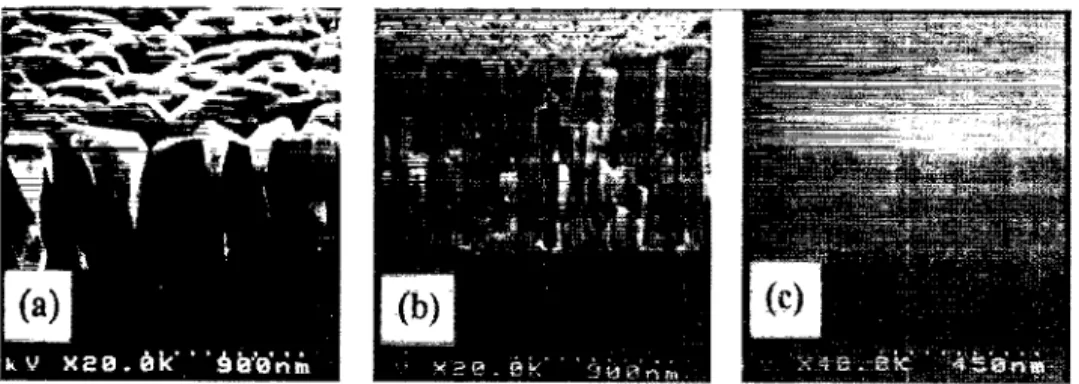
The resistivity and deposition rate of the blanket W-film varies with WF,/SiH, flow rates. Fig. 1 shows that both the resistivity and the deposition rate increase with increasing SiH, flow rate at a constant WF, flow rate of 20 seem. The larger amount of Si incorporated into the W-film is presum- ably responsible for the higher resistivity [ 6]. Grain struc- tures of the blanket W films deposited with different WF,/ SiHj flow rate ratios are fairly different, as shown in Fig. 2. The X-ray diffraction patterns of the W films deposited on bare Si with different WF,/SiH, flow rates are illustrated in Fig. 3. The Q-W signals were detected on the films deposited with lower the SiH, flow rate of 10 seem (Fig. 3(a) ) , while the 0-W signals were detected on the films deposited with the higher SiH, flow rate of 30 seem (Fig. 3(b) ) . The LY-W phase, which has the b.c.c. type-A2 lattice, is desirable for ULSI application because it is thermodynamically stable and exhibits the lowest resistivity among all crystalline phases of tungsten [7]. The 0-W phase has a cubic, type-Al5 lattice, and is metastable below 630°C IS]. For the WF6/SiH, flow rate ratio less than I/2, amorphous WSi, film was obtained (Fig. 3(c)) and the deposition selectivity was lost com- pletely [ 91.
Fig. 4 shows the half-filled and overfilled contact holes of 1.0 pm size using selective CVD-W technique. Excellent selectivity, good uniformity, and low resistivity W can be
30 t 25 g 20 3 6 15 $ 10 5 +Dcposltloa Rate 1200 1200 1 1 s s 900 900 8 8 w w 600 600 T$ T$ 300 300 s- s- B B 3 0 5 10 15 20 25 30 35 35 5 1500 g 1500 g
SiH, flow rate ( seem )
Fig. 1. Resistivity and deposition rate of blanket CVD-W vs. SiH, flow rate at a lixed WF, flow rate of 20 seem.
J
20 30 40 50 60 70 80
28
Fig. 2. XRD spectra of tungsten films deposited on bare Si substrate with WF,/SiH, Aow rates of (a) 20110, (b) 20/30 and (c) 2/30 seem, respectively.
I Marerids Chemisr~ and Physics 51 (I 997) 75-79 77
Fig. 3. Scanning electron micrographs showing different structures of blanket tungsten films deposited with WF,/SiH, flow rates of (a) 20110 seem, (b) 20/ 30 and (c) 2/30 seem, respectively.
Fig. 4. (a) Half-filled and (b) overfilled contact holes with size of 1.0 km using selective CVD-W process.
obtained with the WF,/SiH, flow rate of 20/ 10 seem. Thus, the WF6/SiHS flow rate of 20110 seem was used to deposit tungsten for CMP study in this work. Compared with the blanket W, the total volume of W that needs to be removed during the W-CMP process is very small for the selective CVD-W, as shown in Fig. 5. Only a small volume of the nail heads due to overgrowth and some W-particles on the surface of dielectric due to selectivity loss need to be removed. The belly-shaped vias were formed as a result of the different etching rate between SOG and PECVD oxide during the via etching [ 41.
CMP was firstly applied to polish the blanket tungsten films with a thickness of 8000 A. A very smooth surface can be obtained at a down-pressure of 3 psi and a back-pressure of 2 psi with a removal rate of 1400 A min- ‘. Before CMP, the tungsten film has a rough surface, as shown in Fig. 6(a) ; the
surface roughness was flattened and a scratch-free surface was obtained after the CMP process, as shown in Fig. 6(b)
Fig. 7 shows the results of a processing series of pattern definition (Fig. 7 (a) ) , selective CVD-W (Fig. 7 (b) ) , W- CMP (Fig. 7(c) ) , and post-CMP cleaning (Fig. 7(d) ) in sequence performed for 0.6 p,m trenches. The overgrowth of CVD-W on the trenches was completely removed after a 30 s W-CMP process; however, some abrasive particles ( A1203) remained, as shown in Fig. 7 (c) . A dilute ammonia solution (0.6%) was used to remove the contamination from slurry and/or from dirty CMP environments. With such a post-CMP cleaning step, no abrasive particle residues can be observed, as shown in Fig. 7(d) [ 10,l l] . Increased ammonia content in the solution tends to induce corrosion of tungsten; Fig. 8 shows a serious corrosion of tungsten following a 120 s post- CM-Pcieaning in a 5% ammonia solution.
Fig. 5. The total volume of tungsten films needs to bc removed during W-CMP process is smaller for (a) selective CVD-W, as compared with (b) blanket
MT. Wcmg et (11. /Mc&v+ais Chemistry awl Phgics 51 (1997) 75-79
Fig. 6. Scanning electron micrographq showing the surface of a blanket tungsten film (a) before, and (b) after a CMP process.
Fig. 7. Scanning electron mtcrographs showing the results of a series of processing in sequence: ia) pattern definition, (b) selective CVD-W, (c) W-CMP process, and (d) post-CMP cleaning. The pattern contains 0.6&m trenches.
Fig. 8. Scanning electron micrographs showing a serious corrosion of tung- sten resulting from a 120 s post-CMP cleaning in a 5% ammonia solution.
The overfilled nail heads of selective CVD-W and the tungsten particles deposited on the surface of dielectric due to selectivity loss can be removed effectively even using a very low down-pressure of 3 psi in a very short polishing
time of 30 s. The lower down-pressure of W-CMP reduces surface roughness and extends pad lifetime, and the shorter
wafer edge center edge
Fig. 9. Removal rate selectivities of W to barrier metals.
polishing time promotes throughput of CMP and reduces consumption of slurry; thus, the process cost of W-CMP can be reduced effectively. The removal rate selectivities of W to various dielectrics and barrier metals were also evaluated with the CMP process performed under the conditions shown in Table 2. The removal rates of thermal oxide, PECVD-TEOS, and BPSG were found to be 30,4.5 and 95 A min-‘, respec- tively: thus the removal rate selectivities of W to thermal oxide, PECVD-TEOS, and BPSG were determined to be
79
47:1, 3O:l and 1.5: 1, respectively. The removal rates of the barrier metals of TiW, Ti and Ta were found to be about 2300, 240 and 5OA min-‘, respectively. These removal rates together with those of W measured at various positions across a 6 in substrate are illustrated in Fig. 9. The removal rate selectivities of W to TiW, Ti, and Ta were determined to be 0.6:1, 6:l and 28: 1, respectively, in the center part of sub- strate. The results of this study indicate that this novel process is very promising for ULSI multilevel interconnection application.
4. Conclusions
A novel process that combines selective CVD-W with the W-CMP technique was developed. This novel process not only improves the throughput of W-CMP dramatically, but also extends the pad lifetime and reduces the consumption of slurry; thus, the process cost of W-CMP can be reduced. Overfilled nail heads and selectivity loss can be removed effectively using a very low down-pressure of 3 psi in a very short polishing time of 30 s. The lower down-pressure of W- CMP reduces surface roughness and extends pad lifetime, and the shorter polishing time promotes throughput of CMP and reduces consumption of slurry; thus, the process cost of W-CMP can be reduced effectively. Furthermore, the removal rate selectivities of W to thermal oxide, PECVD- TEOS, and BPSG were found to be 47:1, 30: 1 and 15:1, respectively. These results indicate that the novel process
developed in this study is very promising for ULSI multilevel interconnection application.
Acknowledgements
This work was supported by the National Science Council (ROC) under Contract No. NSC85-2215-E-009-068.
References
[ 11 F.B. Kauffman, D.B. Thompson, R.E. Broadie, M.A. Jaso, W.L. Guthrie, D.J. Pearson and M.B. Small, J. Electrochem. Sot., 138 (1991) 3460.
[2] M.A. Fury, Solid StateTechnol., 38 (April 1995) 37; 38 (July 1995) 81.
[3] W.K. Yeh. M.C. Chen andM.S. Lin, J. Electrochem. Sot., 142 (1995) 3582.
[4] W.K. Yeh,T.C. Chang, K.Y. Chan andM.C. Chen, Jpn. J. Appl. Phys., 35 ( 1996) 1115.
[5] W.Y. Yeh, M.C. ChenandM.S.Lin,J.Vac. Sci.Technol.B, 13 (1996) [ 61 J.E.J. Schmitz, Chemical Vapor Deposition of Tungsten and Tungsten Silicides for VLSI/ULSI Applications, Noyes, Park Ridge, NJ, 1991, p. 63.
[ 71 W.B. Pearson, Handbook of Lattice Spacings and Structures of Metals and Alloys, Pergamon, London, 1958, p. 883.
[8] C.J. Smithella, Metals Reference Book, London, 1955, p. 195. [9] M.L. Yu and B.N. Eldridge, J. Vat. Sci. Technol. A, 7 (1989) 1441. [lo] S.R. Roy, I. Ali, G. Shim, N. Furusawa. R. Shari, S. Peterman, K. Witt
and S. Eastman, J. Electrochem. Sot., 132 (1995) 216.
[ 111 T.L. Myers, M.A. Fury and W.C. Krusell, Solid State Technol., 38 (October 1995) 59.