Develop a novel thermal switch through CMOS
MEMS fabrication process
You-Liang Lai1, Lei-Chun Chou2, Ying-Zong Juang1, Hann-Huei Tsai1, Sheng-Chieh Huang2, Jin-Chern Chiou2 1. National Chip Implementation Center (CIC), Hsinchu, Taiwan 300, R.O.C
2. Dept. of Electrical Control Engineering, National Chiao Tung University, Hsinchu, Taiwan 300, R.O.C E-mail: [email protected]
Abstract- This paper focuses on implementing two novel CMOS-MEMS type switches: buckling type and thermal type, by using commercially available TSMC 0.35 μm two-poly four-metal (2P4M) CMOS process. There are two novel designs in these two type switches: first, the soft contact structure with post-processing fabrication; second, using residual stress to achieve large structural deformation in buckling type and thermal type switches. To create the soft contact structure, residual gradient stress effect has been utilized to make bending-down curvatures. According to the experiments, the layer Metal1 has the largest negative residual gradient stress [1] effect that can achieve the largest negative deflection in z-axis. Because the structure will bend down after post-processing release, larger lateral contact area are set up to gain the lower contact miss ability. In the post-processing fabrication, 0.3μm thickness gold will be deposited on the contact tips. Due to the essence of gold, comparing with aluminum, has no oxidation issue, gold also has the advantage of higher conductivity to reduce the electrical power loss. In the buckling type design, the switch uses residual stress to achieve lateral buckling effect to solve long distance problem. In the thermal type design, this paper design a folded-flexure [2, 3] with the electro-thermal excitation to turn the switch on or off. In the prototype, the device size is 500 μm × 400 μm and the gap between two contact pads is 9 μm in off-state. on the experimental results, the switch can work stably at 3 volts, and the displacement of the thermal type switch can achieve 2.7μm, which is sufficient for the mechanism of switching-on or switching-off.
I. INTRODUCTION
CMOS MEMS utilizes the CMOS stacked layers to form the micro-sensors and the micro-actuators. It has great potential for commercial production. However, stacked CMOS layers are composed of compound materials like metal, via, poly-silicon, and oxide layers. There is stress in and between these layers. The extraction for individual layer in CMOS spends large chip area. And the simulation time for microstructure with the complicated multi-layers is much longer by using this method. The efficient method is to extract the effective mechanical properties of some basic metal/oxide combination structures. It not only costs less testing area and simulation time but also includes the stress of interlays. This paper used the effective mechanical properties extracted from eight combinations of CMOS metal/oxide stacked structures to simulate and predict the static and dynamic behavior of MEMS device. The problem of the lateral contact switch has been solved in this study by depositing gold on the Aluminum layer.
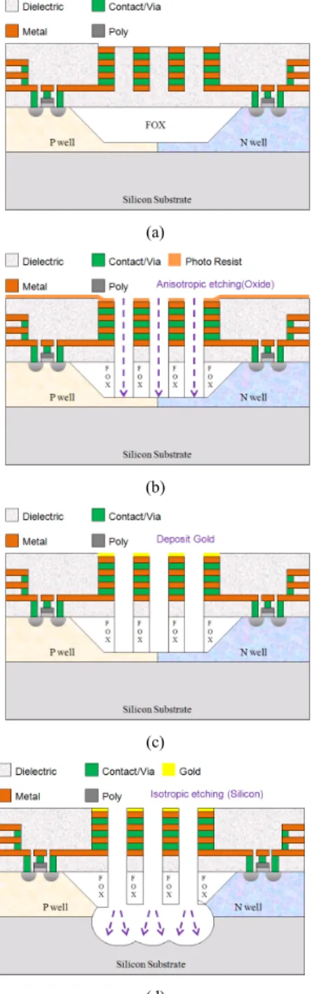
II. FABRICATION
The CMOS MEMS multi-project wafer (MPW) was fabricated by TSMC 0.35 μm two-poly four-metal (2P4M) CMOS process and CIC micromachining post process. The major materials of metallization and dielectric layer in this CMOS process are respectively aluminum and silicon oxide. Fig. 1 shows the cross-section views of the MPW with post-CMOS micromachining steps. By the way, in this study we use Bio CMOS MEMS process, a gold layer is deposited on top layer.
For alleviating the dry etching process on dielectric layers, as Fig. 1(a) shows, the CMOS passivation layers on etching selective regions are removed during the CMOS process. Before the anisotropic dry etching, an additional photo-resist layer is spun and lithographed on the wafer for the post-process. This lithography enables the definition of the protective region of photo-resist layer over the metal of the inductor. The thickness of the photo-resist requests at least 5μm to avoid the RIE etching directly on the top meal. The anisotropic RIE etching with CF4, CHF3 and O2 is subsequently used to remove the exposed dielectric oxide in Fig. 1(b). In this step, most photo-resist layers would exhaust with the RIE gas. When all metal layers are done, a gold layer is deposited on the top layer, as seen in Fig. 1(c). As Fig. 1(d) indicates, the following isotropic dry etching with SF6 and O2 is then included to remove the underlying silicon substrate and release the microstructures.
(a)
(b)
(c)
(d)
Figure 1 Post-CMOS micromachining steps: (a) after completion of CMOS, (b) protective photo-resist layer and anisotropic dry oxide etching, (c) a gold layer is deposited on top layer, and (d) the isotropic dry silicon etching and structural release.
III. DEVICE DESIGN
In this paper, there are two types novel CMOS-MEMS switches by using commercially available CMOS process (TSMC, 2P4M) [4] has been proposed. There are two designs should be discussed: the unique soft contact structure and post-processing fabrication, a buckling actuator design in buckling type and a new thermal actuator design in thermal type.
A. The soft contact structure
In a normal switch design, the contact area is so small as to make a poor contact (Fig. 2). To solve this problem, we design a new contact profile which used negative residual gradient stress effect and the different configurations of the contact tip.
Figure 2. Cross-section view of normal contact profile.
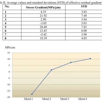
Every metal used in the TSMC 0.35 μm 2P4M CMOS process has different effective residual stress. Combine different metal layer also can get different residual gradient stress. Table 1 shows eight combinations of CMOS metal/oxide stacked structures [1]. Table 2 is the average values and standard deviations of effective residual gradient stress.
Table I. Eight combinations of CMOS metal/oxide stacked structures.
No. Metal 1 Metal 2 Metal 3 Metal 4 1 ● ● ● ● 2 ● ● ● 3 ● ● ● 4 ● ● ● 5 ● ● 6 ● ● 7 ● ● 8 ●
Table II. Average values and standard deviations (STD) of effective residual gradient stress.
No. Stress Gradient(MPa/μm) STD
1 4.35 3.83 2 21.92 7.48 3 2.90 3.84 4 -3.05 3.03 5 20.48 7.83 6 12.45 6.00 7 -5.42 3.90 8 10.39 4.85
Figure 3. Effective gradient stress vs. metal layer.
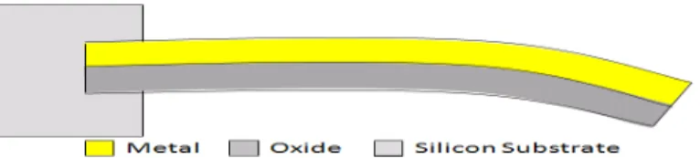
By comparing Table II, only the layer metal 1 has the negative residual gradient stress (Table 2, Fig. 3). Therefore, with metal 1 in contact structure, the contact profile will bend down after release (Fig. 4). With this profile, it provides
lager lateral contact area than the normal design. However, this method also increases the distance between two contact areas, therefore, large lateral displacement in contact area is needed when designing the switch.
Figure 4. Cross-section view of proposed contact profile.
This study also designs different configurations of the tip with different contact profile which can get more lateral contact area than normal design (Fig. 5a, 5b).
Figure 5(a). Cross-section view of normal contact tip.
Figure 5(b). Cross-section view of proposed contact tip.
In the post-processing, 0.3μm thickness gold will be deposited on the surface of the element as shown in Fig.1(c). Since gold is non-active, it has more reliability on avoiding the problem of oxidation and increasing the conductivity at contact area.
B. New design of switched
Type I. A new design of thermal actuator
In the new thermal actuator design, this paper proposed a novel folded-flexure with the electro-thermal excitation to turn the switch on or off, as seen in Fig. 6. By comparing Table III, the stress increases with the numbers of metal layers, as shown in Fig. 7. It indicated that oxide layer in CMOS process has compressive stress and the metal layer has tensile stress. This paper used a lateral bimorph beam structure, as illustrated in Fig. 6(a).After post-processing release, the beam will be lateral bending to metal side, as shown in Fig. 6(b).
When applying the voltage to make the switch turn on, there is heat generated due to electrical current pass by the switch. Because the thermal coefficient values of oxide and aluminum are 0.4 * 10-6/K and 23 * 10-6/K individually. [5] The folded-flexure of the thermal type switch will pull back when applying voltage. Thus the switch will turn off, as shown in Fig. 6(c). Therefore, the folded-flexure structure is designed to control the switch turn on or turn off.
Figure 6(a). Top view of micro-cantilever beam before release.
Figure 6(c). Top view of micro-cantilever beam. Due to different thermal Coefficient, the structure will pull back with applying voltage. Table III. Average values and standard deviations (STD) of effective gradient stress property.
No. Stress Gradient(MPa/μm) STD
1 64.27 4.43 2 27.79 4.74 3 40.45 7.33 4 38.88 4.79 5 13.23 1.26 6 7.97 2.67 7 20.35 1.45 8 -20.96 3.07
Figure 7. Effective residual stress vs. numbers of metal layer. Type II. A new design of buckling actuator
In the new buckling actuator design, this paper proposed a novel switch design by using buckling effect. By
comparing Table III [1], the stress increases with the numbers of metal layers, as shown in Fig. 7. Thus the oxide layer is compressive stress and metal layer is tensile stress. But buckling effect can cause the structure deform in two directions, as shown in Fig. 8(a). Thus this paper uses another way to make sure the deformation is the same as expectation after the structure was released, as seen in Fig. 8(b).
Figure 8(a). Top view of buckling effect after release. Figure 8(b). Top view of proposed design by using buckling effect. P is the compressive stress. P is the compressive stress
In order to control the switch turning on or off, the beam of the buckling type switch bends down when applying voltage, as shown in Fig. 9 (a) and Fig. 9(b).
Figure 9(a). Cross-section view of the switch at initial time, the switch turns on without applying voltage.
Figure 9(b). Cross-section view of the switch after applying voltage, the beam bends down and the switch turns off.
IV. EXPERIMENTAL RESULT
The Fig. 10(a) is the layout of buckling type switch and the Fig .10(b) is the layout of thermal type switch.
The right red square in Fig .10(a), is the beam using buckling effect used to get large displacement after the structure was released. The switch is initial at on state after post-processing. The white square, as shown in Fig. 10(a), is the thermal beam. This part is used to control the switch turn on or off. The beam of the buckling type switch will bend down when applying voltage. Thus the switch will turn off.
In Fig. 10(b), the top right red square is the folded-flexure used to get large displacement after the structure was released. The switch is also initial at on state. The folded-flexure part is also used to control the thermal type switch turn on or off. When applying voltage, the folded-flexure pulls back and the switch turns off.
These switches were fabricated by using TSMC 0.35 μm 2P4M CMOS process and CIC post micromachining process. In the prototype, device size is 1300 μm * 1300 μm in buckling type and 500 μm * 400 μm in thermal type. In the measurement, we use MEMS motion analyzer (MMA), scanning electron microscope (SEM) and Optical Microscope (OM) to measure the profile and characteristic of the device. The measurements include static state and dynamic state.
Figure 10(a). The layout of the buckling type switch. Figure 10(b). The layout of the thermal type switch.
In the static state, this paper use probes to apply voltage and control signal. Fig. 11(a) is the full view of the buckling type switch photo by SEM. The contact area of the switch bends down due to residual gradient stress, as seen in right figure in Fig .11, the tip of the contact area bends down approximately 21μm. The result shows that the residual gradient stress can successfully use to make bend down structure, therefore, lager contact area can be achieved.
Fig. 12 is the buckling type switch photo by OM. The lateral displacement in the center of buckling effect part is 16.5 μm approximately. As shown in Fig .11(b), the lager lateral displacement is achieved by using buckling effect method.
Fig. 13 is the thermal type switch by OM, the length of the gap is 21 μm. By comparing the initial layout, the lateral displacement of center gap is 15.4 μm. The experimental result shows large displacement can also be achieved by lateral bimorph beam structure.
Figure 11. Full view of the buckling type switch by SEM.
Figure 12. One side of the buckling type switch.
Figure 13. One side of the thermal type switch.
Fig. 14 is the correlation between displacement of the contact-tip and input voltage. The voltage source between the contact profiles are 0 V to 3 V, and the maximum displacement of dynamic motion is about 2.7μm.
Figure 14.Contact-tip of the thermal type switch displacement vs. voltage.
V. CONCLUSION
In this study, two new type switches, buckling type and thermal type, were proposed and implemented by using TSMC 0.35 μm 2P4M CMOS process and CIC micromachining post process. These two type switches used the residual stress effect to get two results as expectation: first, contact-tip will bend down approximately 21μm in buckling type switch; and second, large lateral displacement is achieved after structure was released. The lateral displacements of buckling type and thermal type switch are 16.5 μm and 15.4 μm individually. In the prototype, device size is 1300 μm * 1300 μm in buckling type and 500 μm * 400 μm in thermal type. According to the measurement result and the photo by OM, the switch can work stably at 3 volts, and the maximum displacement of dynamic motion is about 2.7μm.
ACKNOWLEDGMENT
The author would like to thank National Chip Implementation Center (CIC) which given a well research resource to help us developing the device.
REFERENCES
[1] Y.L.LAI,Y.Z.JUANG,S.C.HUANG,S.H.TSENG,H.H.TSAI,“Effective Mechanical Properties Measurements in Standard CMOS Process,”
Asia-Pacific Conference on Transducers and Micro-Nano Technology (APCOT2010) Perth, WA, June 2010, pp. 126.
[2] A.Oz, G. K. Fedder, “RF CMOS-MEMS capacitor having large tuning range,” in Proc. 2003 IEEE Int. Conference on Solid-State Sensors and
Actuators (Transducers ‘03) Boston, MA, June 2003, pp. 851-854.
[3] A.Oz, G. K. Fedder, “CMOS/BiCMOS Self Assembling and Electrothermal Microactutors for Tunable Capacitors, Gap-closing Structures and Latch Mechanisms,” 2004 Solid-State Sensor, Actuator and Microsystems Workshop, Hilton Head Is., SC, pp. 212-215.
[4] The CIC CMOS MEMS Design Platform for Heterogeneous Integration, Technical Report, CIC-CID-RD-08-01, V1.0, National Chip Implementation Center, Hsinchu, Taiwan, April, 2008.