This content has been downloaded from IOPscience. Please scroll down to see the full text.
Download details:
IP Address: 140.113.38.11
This content was downloaded on 28/04/2014 at 20:09
Please note that terms and conditions apply.
Characteristics of titanium silicide formed by Si/Mo/Ti trilayer metallisation
View the table of contents for this issue, or go to the journal homepage for more 1989 Semicond. Sci. Technol. 4 177
(http://iopscience.iop.org/0268-1242/4/3/007)
Semicond. Sci. Technol. 4 (1989) 177-183. Printed in the UK
Bi-Shiou Chiout, Biing-Jang Yangt and Peng-Heng ChangS t Institute of Electronics, National Chiao Tung University, Hsinchu, Taiwan, Republic of China
*
Central Research Laboratory, Texas Instruments, Dallas, TX 75265, USA Received 26 July 1988, in final form 19 October 1988, accepted for publication16 November 1988
Abstract. The Si/Mo/Ti trilayer structure exhibits good oxidation resistance. The tormed titanium silicide possesses a low resistivity of 16pQ cm after annealing for 30 min at 750 "C and good stability for wet and dry oxidation at tempera- tures above 900 "C. The barrier height of titanium silicides increases slightly a s the annealing temperature is raised above 600 "C, and is about 0.6 eV at 750 "C for both the n-type and p-type substrates. With As' (or BF;) ion implantation to increase t h e surface concentration of n-type (or p-type) substrate, t h e effective barrier height can be reduced to about 0.4 eV for an implantation dose of 1 . 0 ~ IO" cm-'. By means of As: (or BF;) ion implantation to introduce a thin inversion layer on p-type (or n-type) silicon substrate, the effective barrier
height is increased to about 0.9 (or 0.82) eV for a dose of 1 X 10'' cm-'.
1. Introduction
Refractory-metal silicides with low resistivities and high stabilities have been under active investigation as inter- connect and electrode materials for very-large-scale integration (VLSI) circuits [l-51. Among them, TiSiz is
probably the most attractive candidate for self-aligned silicide (salicide) application [4, 51. It has relatively low resistivity (15-2OpQ cm) and high thermal stability. Nevertheless, due to the high oxidation rate of Ti to some oxidants even by two-step annealing [6], the quality of the resultant TiSiz is very sensitive to oxidis- ing gases in the sintering atmosphere. The undesired oxidation results in a non-uniform silicide formation and non-uniform etching due to variations in the oxidised Ti surface across a wafer. Park et a1 [7] pro- posed a Mo/Ti bilayer structure to solve this problem. However, as oxidants may penetrate the top MO layer to react with the bottom Ti layer, it still requires some degree of ambient control. Lin er a1 [8] suggested a Si/Mo/Ti trilayer structure to overcome this problem. It is reported that a top Si layer can prevent the residual oxidants from reaching the bottom Ti layer and that an MO layer can eliminate the undesired reaction between Si layer and Ti layer.
Silicides are attractive for gate metallisation because of the possibility of forming silicides directly on polysilicon, thus preserving the basic polysilicon MOS
gate while decreasing the resistance. Hence, it is important to examine the compatibility and stability of titanium silicide as it is formed on polysilicon gate. In this work, the compatibility of TiSi, with polysilicon gate is studied on the basis of the Si/Mo/Ti structure for
TiSiz formation as mentioned above. Oxidation proper- ties of Ti silicide are examined in dry and wet oxygen atmospheres. Results of investigation on Schottky bar- rier heights for TiSiz contacting with ion-implanted silicon substrate are presented. This is aimed at poten- tial applications in using a silicide-n-p (or silicide-pn) Schottky barrier structure for solar cell and other IC
usage [9].
2. Experimental procedures
For several experiments in this study, (100) n-type wafers with resistivity of 2-4 Q cm were employed. Wafers were first oxidised to form a 500-1000
A
SiOz layer. A 2000P\
polysilicon layer was then deposited by LP CVD and doped by POCI:, diffusion. A trilayerstructure which consists of
-400
A
Ti, -500A
MO and -10008, Si films was successively deposited with an ETE CL680 Dual E-gun multiple-crucible evaporator at -1O-6 Torr. For comparison, the trilayer structure was also deposited directly on the single-crystal silicon substrate of the same type and orientation. The film thickness was controlled by a IC 2000 thicknessmonitor. Several samples were then annealed in an N2-flowing (5000 cm3 min") open-tube furnace from 550 to 1000 "C in 50 "C increments for 30 min, and other samples at 600 or 750 "C from 10 to 180 min to examine the change of sheet resistance with time.
After annealing the top Si layer of the samples was removed by CF,/Oz gas-plasma etching. The MO layer and the unreacted Ti were then etched in a solution of NH,0H:HzOz:H20= 1:15 in molar ratio for 20 min.
Bi-Shiou Chiou et a/
The sheet resistance of the samples was measured with the four-point probe. The structural and morpho- logical development of the samples was analysed with an x-ray diffractometer (Shimadzu XD-5), scanning electron microscope (Hitachi S-570), transmission elec- tron microscope (JEOL 100-CXII) and Rutherford back-scattering (RBS) technique.
Samples annealed at 750°C for 30 min were oxidised in dry or wet 0' atmosphere from 700 to 1100°C in 100°C increments for 1 h after the removal of the Si/Mo layer. The sheet resistance of these sam- ples was then measured again with the four-point probe, and microstructures were analysed with SEM, TEM and x-ray diffractometer.
In some other experiments, both (100) n-type (4-7 S2 cm) and (100) p-type (6-20 S2 cm) wafers were used. Wafers were first oxidised to form an Si02 layer of -4200
A
for passivation. The oxide on the back side was then removed. POC13 diffusion was performed on the n-type wafers to improve the ohmic contact on the back side. The front side of the SiOz layer was pat- terned into circles with a diameter of 350pm.Before ion implantation, a 620A S O 2 layer was grown on the patterns as the barrier layer. Arsenic was implanted through the barrier layer on the n-type wafers at an energy of 140 keV with a dose ranging from 1.0
x
1OI2 to 1.0 x 10'' As+ cm-'. The same energy was applied on the p-type wafer, but with a dose in the range of 1 . 0 ~ 10" to 1.0 x lO"As+ cm-2. Boron implantation was performed on the n-type wafers at an energy of 90 keV with a dose ranging from 1.0 X 10" to1.0 X 10l2 BF'cm-'. On the p-type wafers, the same energy was used but with a dose in the range of 1.0 X 10" to 1.0 X l O I 5 BF2 cm-'. All the wafers were then annealed at 900 "C for 30 min in O2 ambient to activate the dopants. The active area of the diodes was defined again by aligning to the original patterns and the SiOz barrier layer was removed by buffer oxide etching (BOE). The trilayer structure was deposited and patterned by the lift-off technique. In this scheme,
7n'6;L-"
c"
-
12g
8- 0 Ln m -c -- ? c 111;
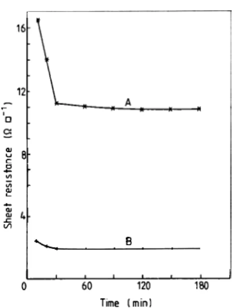
4 - t, B 1 I 0 60 120 180 Tlme lminlFigure 1. Sheet resistances of titanium polycide as a function of sintering time in N2 atmosphere at temperatures of: A, 600 "C; B, 750 "C.
positive photoresist was used as mask material, and the trilayer structure was deposited in a vacuum chamber at a temperature of about 20°C by a dual e-gun. The sintering of the samples was performed in an Nz-flowing (5000 cm3 rnin") open-tube furnace at tem- peratures from 600 to 900 "C in 50 "C increments and then the Si and MO layers were removed as described above.
Finally, an aluminium film of about
6OOOA
was deposited onto the back side of the wafers and sintered at 400°C for 20min. Current-voltage (I-V) measure- ments were performed on these diodes with a semicon- ductor parameter analyser (Hewlett Packard HP4145). 3. Results and discussionFigure 1 shows the plot of the sheet resistance R, for titanium polycide after the top Mo/Si layers were removed as a function of sintering time at 600 and
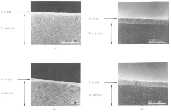
Figure 2. SEM micrographs of titanium silicides formed by sintering the SilMolTi trilayer structure on silicon at 600 "C for ( a ) 10 min, ( b ) 20 min and (c) 30 min in N2 ambient.
Characteristics of titanium silicide
Figure 3. SEM cross-section micrographs of titanium silicides formed by sintering the Si/Mo/Ti trilayer
structure on silicon at 600 "C i n a N2 atmosphere for ( a ) 10 min, ( b ) 20 min, (c) 30 min. ( d ) 120 min.
750°C. At both temperatures, R, decreases with time and eventually reaches a minimum value after sintering for longer than 30 min. This is similar to that reported by Murarka and Fraser. For less than 20 min sintering at 600°C. neither silicide formation nor grain growth is observed, as shown in figures 2 ( a ) and ( h ) . After 30 min annealing, the grain becomes larger a s pre- sented in figure 2(c). and TiSi crystalline phase is detected by the x-ray diffraction [6]. The formation of
silicide causes the low sheet resistance as shown in figure 1 . Figure 3 presents a cross-sectional view of titanium silicide film annealed at 600°C for different times. I t is interesting to note that the thickness of the titanium silicide seems to be the same for samples annealed for longer than 30 min. as shown in figures 3(c) and ( d ) . This implies that after 30min annealing at
6OO"C,
the reaction between the Ti film and the silicon is nearly accomplished. This is consistent withFigure 4. TEM cross-section of TiSiz polycide gate. The silicide was formed by sintering the trilayer structure Si/Mo/Ti on doped polysilicon at 750 "C for 30 min in a N2 atmosphere.
Bi-Shiou Chiou et a/
600 700 800
Temperature PC)
Figure 5. Plots of sheet resistances of titanium silicides as a function of the sintering temperature for 30 min in a N2 atmosphere by depositing a trilayer structure Si/Mo/Ti on: A, single-crystal silicon; B, doped polycrystalline silicon.
the trend in sheet resistance as presented in figure 1. Besides, it can be seen that the microstructure of the silicide consists of columnar grains.
The TEM cross section of TiSiz polycide gate is
represented in figure
4.
The silicide was formed by sintering the trilayer structure Si/Mo/Ti on doped poly- silicon (18 S2 0") at 750 "C for 30 min in N2 atmos- phere. The polysilicon layer has a columnar structure which is a typical characteristic observed in the as- deposited polysilicon film. This suggests that the annealing treatment, i.e., 750°C for 30min, does not induce any grain growth in the polysilicon layer. A silicide film of about 8008,
is formed at the surface of poly-Si with a wavy polysilicon interface. TEM investi-gation of this sample indicates that there is a weak diffraction contrast in this layer, which is believed to be
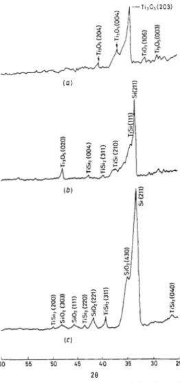
l I , l , I / 0 800 1600 2400 3200 4000 6800 A : SiO, -Tetragonal 0 ' MoSi,-Tetragonal o : MosSi3-Tetragonal x : Tisi, -Orthorhombic t I 60 50 4 0 30 2 8
Figure 6. X-ray diffraction pattern for the sample derived from the Si/Mo/Ti trilayer structure on doped polysilicon gate sintered at 850 "C for 30 min in a N2 atmosphere.
the result from the partial crystallisation of titanium silicide after annealing.
The crystallisation of titanium silicide depends on the annealing temperature. For samples annealed at a temperature lower than 600°C, no crystalline tita- nium silicide that can withstand the etching of (NH,OH+H,O,) is formed. On the basis of x-ray diffraction patterns, it is seen that from 600 to 700 "C, TiSi is the dominant phase along with a small amount of TiSiz present, while from 750 to 800 "C the TiSi phase disappears and only TiSiz exists [6]. The sheet resist- ance as a function of sintering temperature by deposit- ing the trilayer structure Si/Mo/Ti on the single-crystal silicon and doped polycrystalline silicon is given in
I I I G?
I
* ' M O ! ""0° 0 8- "000 I o : T i0
A m : O o o o o o o o o o ~ o ~ Q Q ~ 1 0 0 0 01 I 1 0 1 00 l 0 6-o l l " O 0 " 0.Lt
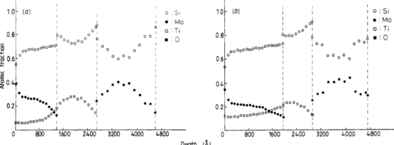
Depth ( h )Figure 7. Depth profiles of the elements Si, MO, Ti and 0 calculated from corresponding FIBS
spectra for the sample derived from the Si/Mo/Ti trilayer structure on doped polysilicon gate sintered for 30 min in a N2 ambient at ( a ) 900 "C and ( b ) 1000 "C. The vertical lines are the original boundaries between different layers. The discontinuities in atomic fraction are attributed to the different initial concentrations in the deposited layers.
Characteristics of titanium silicide TI305 Ti30S: hexagonal IQ1 A : SiO, -Tetragonal o : TiSi,+Orthorhombic Si(211) SiOI 1 1 1 ' ) I ' I M) 50 40 30 28
Figure 8. X-ray diffraction patterns of titanium disilicide
oxidised in dry O2 for 1 h at ( a ) 700 "C, ( b ) 800 "C and
(c) 1000 "C. The TiSi2 is formed on doped polysilicon at
750 "C annealing for 30 min.
figure 5 . The sheet resistance decreases as the sintering temperature is raised above 600 "C, and a constant R, is obtained at temperatures higher than 750 "C. R, of silicide deposited on doped polysilicon is smaller than that on single-crystal silicon. This may be caused by the leakage current of the low-resistance polysilicon film during four-point probe measurements. It is argued that the formation of TiSi2 at the expense of TiSi results in the decrease of the sheet resistance [lo]. The resis- tivity calculated from R, (=2 S2
0"
in figure 5 ) and sample thickness (-800A)
is about 16pQ cm, which is comparable with the value, 13-16pS2 cm, reported by Murarka et a1 [1,10].When samples are sintered at higher temperatures, i.e., 850°C or above, interdiffusion of MO and Ti results in a mixed layer of MO silicide and Ti silicide on the titanium silicide layer as indicated by x-ray diffrac- tion and RBS analysis results presented in figures 6 and
7, respectively. On the basis of the depth profiles of the elements Si, MO, Ti and 0 calculated from corre- sponding RBS spectra for samples annealed at 900 "C,
and 100O"C, as shown in figures 7 ( a ) and ( b ) , respec- tively, it is found that the out-diffusion of Ti atoms into the MO layer increases as the sintering temperature
L
60 55 50 65 40 35 30 25
28
Figure 9. X-ray diffraction patterns of titanium disilicide oxidised at ( a ) 700 "C, ( b ) 800 "C and ( c ) 900 "C in wet
O2
for 1 h and then etched in BOE for 1 min. The TiSi2 is formed on doped polysilicon a t 750 "C annealing for 30 min.increases. However, since Ti silicide with optimum properties can be obtained at a sintering temperature as low as 750 "C [ l , 2, lo], the interdiffusion of MO and Ti will not come into effect during practical applications.
One important test of the compatibility of a poly- cide structure with VLSI interconnect fabrication is the
ability to grow a self-passivating oxide layer without degrading the polycide or the underlying gate oxide integrity. Figures 8 and 9 are the x-ray diffraction patterns of titanium disilicide after dry and wet oxi- dation from 700 to 1100 "C, respectively, for 1 h. It is found that titanium disilicide decomposes and titanium oxides are formed after both dry and wet oxidations at 700 "C for 1 h as shown in figures 8(a) and 9(a). For wet oxidation at 800 "C, parts of the TiSi2 either reduce to TiSi and form SiOz or decompose to form Si02 and titanium oxides as indicated in figure 9(b). At 900"C, Si02 can be produced on the silicide film without changing the stoichiometry of the titanium disilicide as presented in figure 9(c). It is presumed that at higher temperatures (>900 "C) silicon can diffuse from the Si substrate through the TiSiz to the surface where it reacts with oxygen, and dominates the oxidation mechanism before TiSi2 dissociates [11,12]. Hence, the
Bi-Shiou Chiou er a/
stoichiometry of titanium disilicide is thus preserved. At low temperatures, silicide dissociation dominates to form titanium oxides.
Both wet and dry oxidation seem to induce the grain growth of the TiSi, at higher temperature (>WO "C), as shown in figure 10. Mochizuki et uf [ 131 also reported similar phenomena in molybdenum silicide oxidation. The rough silicide-silicon interface may be caused by different silicon diffusion rates through the silicide layer.
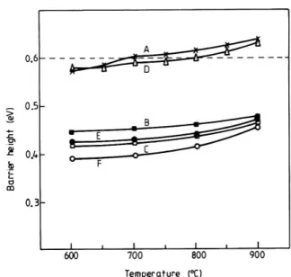
Forming good contact is essential to the operation of the devices. Small barrier height ensures small speci- fic contact resistance. The Schottky barrier height and the ideality factor are obtained from the current-
voltage characteristic of a Schottky diode. Figure 11 is the Schottky barrier height as a function of sintering temperature for titanium silicide formed on n-type and p-type substrates. For the n-type substrate, from 600 to 750 "C, the values of barrier heights are below 0.6 eV, which is comparable with that reported by Cowley et ul [ 1, 141. The slight change with temperature may be attributed to the change of the crystalline phase at the silicide-silicon interface o r due to the associated phase transformation. Above 750 "C, the barrier heights
Figure 10. SEM cross-section micrographs of titanium
disilicide formed on silicon at 750 "C sintering for
30 min: ( a ) before oxidation, ( b ) dry oxidation at 1000 "C for 2 h and (c) wet oxidation at g00 "C for 2 h. 182
Temperature K )
Figure 11. Plot of the Schottky barrier height cpB of
titanium silicide a s a function of sintering temperature. The silicide was formed on: A, unimplanted n-type (100) Si substrate; B n-type (100) Si substrate, As' implanted, dose: 1 x 1014 cm-'; C, n-type (100) Si substrate, As' implanted, dose: 1 x 1015 cm-2; D,
unimplanted p-type (100) Si substrate; E, p-type (100) Si substrate, BF; implanted, dose: 1 x 1014 cm-'; and F, p-type (100) Si substrate, BF; implanted, dose: 1 x
1015 cm-'. The cpe values were calculated assuming the
effective Richardson constant to be equal to the standard value of 120 A cm2 K-*. The average values of
ideality factors n were 1.08 and 1.09 for n-type samples and p-type samples, respectively.
become larger than 0.6 eV and even reach 0.63 eV at 900 "C. It is argued that during sintering a doping level change occurs in the silicon near the silicide-silicon interface [ 151. A similar result is also observed for titanium silicide formed on p-type substrate as demon- strated in curve A of figure 11.
As the Schottky barrier height depends on the doping level at the silicide-silicon interface [16], it can be varied by controlling the doping level in the surface layer of the silicon substrate. Several samples are ion- implanted with As+ (or BF,) ions to study the effect of doping level on Schottky barrier height, and the results are plotted in figure 12. It is observed that the effective barrier height are reduced by 'shallow' implantation of As' into an n-type substrate or by BF, into a p-type substrate. The effective barrier heights of the implanted diodes also vary slightly with the sintering temperatures as shown in curves B , C, E and F in figure 11. This could be explained on the basis of arguments similar to that of the unimplanted diode, in which the dopant concentration changes in the silicon near the silicide-silicon interface during sintering.
The effective barrier height in a TiSi,-p-type (or TiSi,-n-type) silicon Schottky diode is increased by ion implantation to introduce a thin inversion layer on
silicon substrate. Experimental results in figure 12 show that the effective barrier heights increase from 0.6eV for the TiSi?-p-Si (or TiSirn-Si) Schottky diode to 0.9 (or 0.82) eV for a TiSirn-pSi (or TiSi,-pn-Si)
10'2 1013 1 0 1 ~ 10'5
Dose ( c r n - ' ~
Figure 12. Plot of the effective Schottky barrier height
qB of titanium silicide formed on: A, As+-implanted n-type (100) Si wafer; B, BFi-implanted p-type (100) Si wafer; C, As+-implanted p-type (100) Si wafer; D, BFi-implanted n-type (100) Si wafer as a function of dose concentrations. The TiSi2 is formed at 750 "C annealing for 30 min. The
vs
values result from /-V measurement with average ideality factor n being 1.09.Schottky diode with an As+-implanted (or
BF,-implanted) layer and a dose of 1 X 10" cm-'. These data fall in the same range as those of Ti metal-psi (or Ti metal-n-Si) reported by Li et a1 [9].
4. Conclusions
Titanium silicide formed by depositing the SilMolTi trilayer structure on silicon or polysilicon exhibits a resistivity of -16pQ cm when annealed at tempera- tures higher than 750°C. TiSi' is observed to be the phase present to lower the sheet resistance in the Ti-Si system.
For self-passivation and compatibility with polysili- con gate, it is found that at temperatures above 900 "C, a self-passivating oxide layer can be grown without degrading the polycide or the underlying gate oxide
Characteristics of titanium silicide
integrity if the polysilicon beneath the silicide is suffi- ciently thick. At lower temperatures, some titanium disilicide decomposes or reduces to TiSi and titanium oxides are formed for both dry and wet oxidation. Diffusion of Si from the polysilicon layer through TiSiz to the surface to react with oxygen is believed to be the dominant mechanism for SiOz formation at elevated temperatures.
As the titanium silicide contacts with n- or p-type substrates, the barrier height increases slightly as the annealing temperature increases. The barrier height can be controlled by varying the dose concentration. Higher doping by ion implantation can be employed to reduce the barrier height. Enhancement of the effective barrier height in a TiSiz-p-type (or TiSi,-n-type) silicon Schottky diode is achieved by using As' (or BF2) implantation to introduce a thin surface inversion layer between TiSiz and p-Si (or n-Si) substrate.
References
[l] Murarka S P 1983 Silicide for VLSI Applications (New [2] Muraka S P 1980 J . Vac. Sci. Technol. 17 775
[3] Chiou B S, Rau H L, Chang P H and Duh J G 1987
J . Electron. Mater. 16 251
[4] Alperin M
E,
Holloway T C, Haken R A, Gosmeyer C D , Karbavay R V and Parmantie W D 1985IEEE. Trans. Electron Devices ED-32 141
J . Electrochem. Soc. 133 2621
University, Taiwan
Yamahuchi T 1984 J . Vac. Sci. Technol. A 2 259 Soc. 133 2386
Electron Devices ED-27 1310
342
Lett. 42 361 Lett. 40 263
Soc. 127 1128 Jersey: Murray Hill)
[5] Ting C Y, d'Heurle F M, Iyer S S and Fryer P M 1986 [6] Yang B J 1987 M S Dissertation National Chiao Tung [7] Park H K, Sachitano J, Eiden G, Lane E and
[8] Lin M Z, Yu Y C S and Wu C Y 1986 J. Electrochem. [9] Li S S, Kim J S and Wang K L 1980 IEEE Trans. [lo] Murarka S P and Fraser D B 1980 J . Appl. Phys. 51 [l11 d'Heurle F, Irene E A and Ting C Y 1983 Appl. Phys. [l21 Chen J R, Liu Y C and Chu S D 1982 Appl. Phys. [l31 Mochizuki T and Kashiwagi M 1980 J. Electrochem. [l41 Cowley A M 1970 Solid-State Electron. 12 403 [l51 Mochizuki T , Kashiwagi M and Nishi Y 1979 [l61 Sze S M 1981 Physics of Semiconductor Devices 2nd
J. Electrochem. Soc. 126 457C