S0013-4651(98)04-036-1 CCC: $7.00 © The Electrochemical Society, Inc.
As device dimensions in integrated circuits are continuously re-duced, the requirements imposed on advanced metallization become increasingly stringent. These include reducing electrical resistivity, improving electromigration resistance, and avoiding interdiffusion between metal and Si substrate. Copper (Cu) has a very low resis-tivity and excellent electromigration resistance,1,2 and can be de-posited conformably using electroplating as well as chemical vapor deposition (CVD) methods.3–5Therefore, Cu has been regarded as a potential substitute to replace the widely used Al and Al-alloys for advanced metallization. Unfortunately, Cu diffuses fast in Si and forms Cu–Si compounds at temperatures as low as 2008C.6,7In addi-tion, Cu has poor adhesion to interlevel dielectrics and drifts through oxide under field acceleration.8–10Therefore, the use of diffusion barriers between Cu and its underlying layers becomes essential to the successful application of Cu in silicon integrated circuits.
Sputter-deposited refractory metals (such as W, Ta, Mo, and Cr) and their nitrides have become more and more attractive in micro-electronic applications as diffusion barrier materials because of their high thermal stability, good electrical conductivity, and excellent capability of suppressing reactions between Cu and Si substrate.11–25 However, it is difficult to deposit barrier layers with excellent barrier properties in contact holes of submicron dimensions using the sput-tering technique because of potential step coverage problems. In this respect, selective CVD of tungsten (selective CVD-W) is one of the most attractive techniques for filling deep submicron contact holes in ultralarge-scale integrated (ULSI) interconnect applications.26,27The selective nature of the selective CVD-W produces a self-aligned structure and provides a more planar surface for the subsequent met-allization process. Thus, it offers a number of potential advantages, including process simplification and possible cost saving.27
It was reported that a 73 nm thick selective CVD-W film acted as an effective diffusion barrier between Al and Si substrate at 4508C for 30 min.28It was also reported that no discernible reaction took place at the Al/W interface at temperatures up to 5008C for W films de-posited by CVD; however, a reaction occurred at the Al/W interface at 4508C for sputtered W and a WAl12compound was formed.4In a previous study, we found that a selective CVD-W film of 450 nm thickness was able to retain its barrier capability between Al and Si substrate at 5758C for 30 min, and the barrier capability was effec-tively improved to 6258C by an in situ N2plasma treatment on the surface of the selective CVD-W film.30Although these studies have provided much valuable information of selective CVD-W films as a
barrier between Al and Si substrate, little study has been made on the barrier capability of selective CVD-W films against Cu diffusion. In one other previous study, we also found that a very thin WSiN layer can be formed on the surface of chemical vapor deposited WSix (CVD-WSix) layer using an in situ N2plasma treatment, and the re-sultant WSiN/WSixbilayer was found to possess a much better barri-er capability against Cu diffusion than the WSixlayer itself.31Thus, the use of WSiN layers as a Cu barrier is of great interest.
In this study, the barrier capability of selective CVD-W films as well as WSiN/WSix/W stacked layers used as a diffusion barrier be-tween the Cu and Si substrate was investigated. The CVD-W films were selectively deposited to a thickness of about 450 nm using the SiH4WF6 reactant gases, while the WSiN/WSix/W stacked layers were formed by depositing a thin layer of WSix on the CVD-W films by CVD, followed by an in situ N2plasma treatment to form a surface layer of WSiN. We found that the WSiN/WSix/W stacked layer possesses a barrier capability far superior to the single layer of CVD-W film.
Experimental
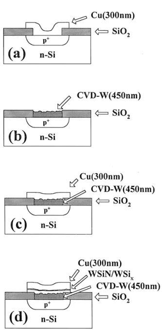
The barrier properties of selective CVD-W films and WSiN/ WSix/W stacked layers were investigated using a structure of Cu/W/ p1-n as well as Cu/WSiN/WSix/W/p1-n junction diodes. The starting material was (100)-oriented, n-type silicon wafers with 4–7V cm nominal resistivity. After RCA standard cleaning, the wafers were thermally oxidized to grow a 500 nm thick oxide layer. Diffusion areas with sizes of 500 3 500 and 1000 3 1000 mm were defined on the oxide-covered wafers using conventional photolithography. The p1-n junctions with junction depth of 0.3 mm were formed by BF12 implantation at 40 keV to a dose of 3 3 1015cm22followed by fur-nace annealing at 9008C for 30 min in N2ambient. After the forma-tion of juncforma-tions, the wafers were divided into four groups for the preparation of the following devices: Cu/p1-n, W(450 nm)/p1-n, Cu/W(450 nm)/p1-n, and Cu/WSiN/WSix(75 nm)/W(450 nm)/p1-n junction diodes. The schematic cross sections of these differently metallized p1-n junction diodes are illustrated in Fig. 1. For the lat-ter three structures of diodes, the contact holes were selectively filled with CVD-W to a thickness of about 450 nm; that is, the 500 nm deep contact holes were nearly filled. This technique offers the advantage of fully self-aligned contacts and barrier formation and also provides a more planar surface for the subsequent metallization process.
Prior to the selective CVD-W deposition, the wafers were dipped in dilute HF (50:1) solution for 30 s followed by a rinse in deionized water for 5 min. The wafers were then loaded into a load-locked coldwall multichamber CVD system (ERA-1000S) within 5 min and transferred by a robot arm to the deposition chamber without expo-sure to the atmosphere. The ERA-1000S is a fully automatic
single-Barrier Capabilities of Selective Chemical Vapor Deposited W Films and
WSiN/WSi
x
/W Stacked Layers Against Cu Diffusion
M. T. Wang,
aL. J. Chen,
band M. C. Chen
a,*
aDepartment of Electronics Engineering, National Chiao-Tung University, Hsinchu, Taiwan bDepartment of Submicron Technology Development, ERSO/ITRI, Hsinchu, Taiwan
This work investigates the barrier capability of W layers as well as WSiN/WSix/W stacked layers against Cu diffusion. The W lay-ers were selectively chemical vapor deposited (CVD) in contact holes to a thickness of about 450 nm using SiH4reduction of WF6. We found that the CVD-W layers functioned as effective barriers against Cu diffusion, and the Cu/W(450 nm)/p1-n junction diodes were able to sustain a 30 min furnace annealing up to 6508C without causing degradation in electrical characteristics. The use of WSiN/WSix/W stacked layers as diffusion layers further improved the thermal stability of Cu/WSiN/WSix/W(450 nm)/p1-n junc-tion diodes to at least 7008C. The WSixlayers were deposited by CVD to a thickness of 75 nm using SiH4/WF6chemistry, and the subsequent in situ N2plasma treatment produced a very thin layer of WSiN on the WSixsurface. This thin WSiN layer was very thermally stable and effective in suppressing Cu diffusion. Failure of barrier capability for the W films was presumably due to inter-diffusion of Cu and Si along grain boundaries of the W films, and the interinter-diffusion was probably enhanced by the formation of WSi2. The formation of WSi2consumed the W layer and Si substrate, resulting in a volume change in barrier layer, which, in turn, developed local defects, such as microcracks and stress-induced weak points, and thus provided fast paths for Cu diffusion. © 1999 The Electrochemical Society. S0013-4651(98)04-036-1. All rights reserved.
Manuscript received April 13, 1998.
wafer CVD system equipped with a cluster of multichambers, in-cluding a load/unload, buffer, and two deposition chambers. The sys-tem employs a robot unit in the buffer chamber for wafer transfer in vacuum. The reactor, made of aluminum alloy, was water-cooled and was kept at a high vacuum base pressure of 1026Torr by a turbo-pump. In this work, the CVD-W films were selectively deposited using SiH4reduction of WF6chemistry at a condition illustrated as
follows: substrate temperature 3008C, total gas pressure 100 mTorr, WF6flow rate 40 sccm, SiH4flow rate 10 sccm, and H2carrier gas
flow rate 1000 sccm; the deposition rate was about 5 nm/s. For the preparation of Cu/WSiN/WSix/W(450 nm)/p1-n junction
diodes, the samples deposited with selective CVD-W were trans-ferred to the second deposition chamber, without breaking the vacu-um, for further deposition of blanket WSixlayers to a thickness of about 75 nm. The WSixwas deposited at the following condition:
substrate temperature 2508C, total gas pressure 12 mTorr, WF6flow rate 2 sccm, and SiH4flow rate 6 sccm; the deposition rate was about
2.5 nm/s. After the CVD-WSix deposition, an in situ N2 plasma treatment was performed on the WSixsurface for 300 s. The N2
plas-ma treatment was performed at 200 W plasplas-ma power with N2flow rate of 80 sccm and a gas pressure of 25 mTorr. According to this scheme, a very thin WSiN layer was formed on the surface of the
WSixlayer (shown later in Fig. 6). Figure 2 shows the process flow
for the Cu/WSiN/WSix(75 nm)/W(450 nm)/p1-n junction diodes. Finally, Cu metallization was applied to all samples except that the group of W(450 nm)/p1-n junction diodes were left as they were without a Cu overlayer for comparison. A 300 nm thick Cu film was sputter deposited in Ar ambient at a pressure of 7.6 mTorr using a dc magnetron sputtering system with a base pressure of 1–2 3 1026Torr and with no intentional substrate heating and bias. After the deposition of Cu films, patterns were defined and Cu was etched using dilute (5 vol %) HNO3, while the WSiN/WSix layer was etched using SF6/N2plasma. To investigate thermal stability of the
diodes, samples were thermally annealed in an N2flowing furnace for 30 min at a temperature ranging from 200 to 8008C. Reverse bias leakage current measurement on the thermally annealed diodes was used to evaluate the barrier capability of various barrier layers. An HP-4145B semiconductor parameter analyzer was used for the measurement, and at least 30 diodes were measured in each case. Unpatterned samples of Cu(300 nm)/Si, W(450 nm)/Si, Cu/ W(450 nm)/Si, and Cu/WSiN/WSix(75 nm)/W(450 nm)/Si
multilay-er structures wmultilay-ere also prepared for matmultilay-erial analyses. Sheet resist-ance of the multilayer structures was measured using a four-point probe. Auger electron spectroscopy (AES) was used to determine the composition of WSixfilms. X-ray diffraction (XRD) analysis was
used for phase identification, and scanning electron microscopy (SEM) was employed to observe the surface morphology as well as the change of microstructure.
Figure 1. Schematic cross sections of (a) Cu/p1-n, (b) W(450 nm)/p1-n, (c) Cu/W(450 nm)/p1-n, and (d) Cu/WSiN/WSix/W(450 nm)/p1-n junction diodes.
Figure 2. Process flow of Cu/WSiN/WSix(75 nm)/W(450 nm)/p1-n junction diodes: (a) selective CVD-W (450 nm) deposition, (b) blanket WSix(75 nm) deposition and in situ N2plasma treatment, and (c) Cu deposition patterning.
S0013-4651(98)04-036-1 CCC: $7.00 © The Electrochemical Society, Inc. Results and Discussion
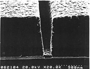
Deposition of Selective CVD-W films and blanket CVD-WSix films.—Figure 3 shows the half-filled and overfilled contact holes of 0.5 mm size using the selective CVD-W technique. Excellent selec-tivity and uniformity of W film deposition was obtained using the SiH4/WF6 chemistry with SiH4/WF6 flow rates of 10/40 sccm. Increasing the SiH4/WF6 flow rates to 20/40 sccm increased the
deposition rate of W but degraded selectivity. Thus, the SiH4/WF6 flow rates of 10/40 sccm were used to deposit CVD-W films for the barrier study in this work. Reducing the SiH4/WF6 flow rates to 6/2 sccm, we obtained blanket CVD-WSix film deposition with
complete loss of selectivity. Figure 4 shows the WSixfilms deposit-ed on submicron trenches with an aspect ratio of 4, revealing a high-ly conformal deposition of CVD-WSix. 32
N2plasma treatment.—Figure 5 shows the results of AES depth
profiles analysis for the WSix films with and without N2 plasma treatment. Without the N2plasma treatment, only a minimal amount
of nitrogen was detected near the WSixsurface (Fig. 5a), presumably due to adsorption of nitrogen gas on the WSixsurface prior to
load-ing the test sample into the AES chamber. After an in situ N2plasma treatment at 200 W for 300 s, a very thin (about 8 nm) WSiN layer was definitely formed (Fig. 5b).
Barrier capability of selective CVD-W films and WSiN/WSix/W
stacked layers.—Electrical measurements.—Barrier capabilities of selective CVD-W(450 nm) films and WSiN/WSix(75 nm)/
W(450 nm) stacked layers against Cu diffusion were investigated by evaluating the thermal stability of Cu/W(450 nm)/p1-n and
Cu/WSiN/ WSix(75 nm)/W(450 nm)/p1-n junction diodes using electrical measurements. Figure 6 illustrates the distributions of reverse bias leakage current density measured at 25 V for the Cu/p1-n, Cu/W(450 nm)/p1-n, Cu/WSiN/WSix(75 nm)/W(450 nm)/ p1-n and W(450 nm)/p1-n junction diodes annealed at various
tem-Figure 3. SEM micrographs showing (a) half-filled and (b) overfilled contact holes of 0.5 mm size using the selective CVD-W technique.
Figure 4. SEM micrographs showing the step coverage of WSixfilms de-posited on submicron trenches with an aspect ratio of 4.
Figure 5. AES depth profiles of as-deposited WSix/Si samples (a) without N2 plasma treatment and (b) with N2plasma treatment at 200 W for 300 s.
peratures. For the diodes without any barrier layer between Cu and Si substrate, the Cu/p1-n junction diodes failed about 2008C anneal-ing (Fig. 6a). With a self-aligned selective CVD-W layer of 450 nm thickness between Cu and Si substrate, the Cu/W/p1-n junction diodes were able to retain device integrity up to 6508C (Fig. 6b). Nevertheless, about a half number of diodes degraded after anneal-ing at 7008C, and all diodes were degraded upon annealing at 7508C. For the junction diodes with a WSiN/WSix/W stacked layer be-tween Cu and Si substrate, the Cu/WSiN/WSix/W/p1-n diodes re-mained stable after annealing at 7008C. Even after annealing at 7508C, about 80% of the annealed diodes retained their leakage cur-rent density less than 100 nA/cm2. This suggests that the barrier capability of the CVD-W layer can be significantly improved by adding an N2-plasma-treated WSiN/WSixbilayer on its surface. It was reported that the amorphous structure of
reactive-sputter-de-posited WSiN layers can be preserved even after annealing at 8508C.33It was also reported that a very thin (4 nm) WSiN layer can be formed on the WSixsurface by ECR N2plasma nitridation and that it functioned as an excellent barrier to dopant diffusion.34In this work, the very thin and thermally very stable WSiN layers gave a great help to suppress the Cu diffusion. Thus, the barrier capability of CVD-W layers was improved.
For comparison, the thermal stability of W(450 nm)/p1-n junc-tion diodes without a Cu overlayer were also measured. The W(450 nm)/p1-n junction diodes retained the integrity of electrical characteristics up to 7008C and revealed only slight degradation after annealing at 7508C; however, severe degradation in electrical char-acteristics was found after annealing at 8008C (Fig. 6d). The degra-dation of W(450 nm)/p1-n junction diodes at 7508C and above was presumably due to a large amount of WSi2formation, as confirmed
Figure 6. Statistical distributions of reverse bias leakage current density for (a) Cu/p1-n, (b) Cu/W(450 nm)/p1-n, (c) Cu/WSiN/WSix/W(450 nm)/p1-n, and (d) W(450 nm)/p1-n junction diodes annealed at various temperatures.
S0013-4651(98)04-036-1 CCC: $7.00 © The Electrochemical Society, Inc.
by XRD analysis (to be shown later in Fig. 7). Since each angstrom of tungsten consumed about 2.53 Å silicon for the formation of 2.58 Å thick WSi2,35the large amount of WSi2formation resulted
in a volume change of the W(450 nm) layer, consumption of Si sub-strate, and probably, a large residual stress. Because the W(450 nm)/ p1-n diodes remained stable up to 7008C, the degradation of Cu/W(450 nm)/p1-n diodes at 7008C was attributed to the presence of the Cu overlayer.
XRD analyses.—Figure 7 shows XRD spectra for the W(450 nm)/Si samples annealed at various temperatures. Only an a-W diffraction peak was detected for the as-deposited sample, as well as those an-nealed at and below 6258C. After annealing at 6508C, weak peaks belonging to the WSi2 phase were detected, indicating reaction be-tween W and Si substrate. However, the small amount of WSi2
forma-tion at the W/Si interface did not degrade the electrical characteristics of W/p1-n junction diodes (Fig. 6d). The peak intensity of the WSi2
phase increased with increasing annealing temperature and the increase in WSi2peaks was also correlated with degradation of
elec-trical characteristics for the W(450 nm)/p1-n junction diodes (Fig. 6d). After annealing at 8008C, the WSi2peaks were further strengthened,
while the a-W peak disappeared, indicating that the W(450 nm) layer might have converted into the WSi2phase completely.
Figure 8 shows XRD spectra for the samples of Cu/W(450 nm)/ Si and Cu/WSiN/WSix/W(450 nm)/Si structures annealed at various
temperatures. For the Cu/W(450 nm)/Si samples, no peak relating to the WSi2phase was observed after annealing at 6008C, indicating
integrity of the samples’ structure (Fig. 8a). After annealing at 7008C, diffraction peaks of the WSi2phase appeared along with a
weak peak of the Cu3Si phase. This indicates that Cu atoms pene-trated through the W(450 nm) layers and reacted with the substrate Si, leading to formation of Cu3Si compound and severe degradation in electrical characteristics of Cu/W(450 nm)/p1-n junction diodes (Fig. 6b). In addition, the formation of Cu3Si compound was proba-bly correlated to the large amount of WSi2 formation at the W/Si
interface. Upon annealing at 7508C, the peaks of Cu(111) and Cu(200) disappeared while the peak of Cu3Si phase was further
strengthened (Fig. 8a). This suggested that the Cu overlayer might have converted into the Cu3Si phase completely.
For the samples of Cu/WSiN/WSix/W(450 nm)/Si structure, though many diffraction peaks relating to the WSi2phase appeared,
no peak relating to the Cu3Si phase was detected, even after
anneal-ing at 7508C (Fig. 8b). This indicated that the WSiN/WSix/W stacked layer effectively suppressed Cu diffusion up to at least 7508C, regardless of the reaction at the W/Si interface. Thus, we may conclude that the barrier capability of the WSiN/WSix/W stacked
layer against CU diffusion is superior to that of a single W layer. Weak diffraction peaks of the W5Si3 phase were observed after
annealing at 650 and 7008C (Fig. 8b), but they all disappeared after annealing at 7508C.
Figure 7. XRD spectra of W(450 nm)/Si samples annealed at various temperatures.
Figure 8. XRD spectra of (a) Cu/W(450 nm)/Si and (b) Cu/WSiN/WSix/ W(450 nm)/Si samples annealed at various temperatures.
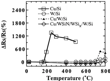
Sheet resistance measurements.—The sheet resistance change in an-nealed samples, normalized to the sheet resistance value of as-de-posited samples, is denoted as DRs/Rs% and defined as follows
Figure 9 shows the percentage change in sheet resistance vs. an-nealing temperature for the samples of Cu(300 nm)/Si, W(450 nm)/ Si, Cu/W(450 nm)/Si, and Cu/WSiN/WSix(75 nm)/W(450 nm)/Si structures. The sheet resistance of Cu/Si remained constant following anneal at temperatures up to 1758C but increased drastically after an-nealing at 2008C. The drastic increase in sheet resistance was attrib-uted to the formation of high-resistivity h0-Cu3Si precipitate and cor-related to the degradation in electrical characteristics (Fig. 6a). For the W/Si structure, the increase in sheet resistance after annealing at 7008C reflects the consumption of conductive W films due to the for-mation of WSi2, as confirmed by XRD analysis (Fig. 7). For the Cu/ W/Si and Cu/WSiN/WSix/W/Si samples, the sheet resistance slightly
decreased with annealing temperature up to 7008C, presumably due to out-diffusion of impurities atoms, grain growth of Cu films, and the heating up of sputter-induced damage in Cu films. Thermal sta-bility of the Cu/W/Si multilayer structure reached 7008C, and a dras-tic increase in sheet resistance was found after annealing at 7508C, implying failure of the Cu/W/Si structure. the drastic increase in sheet resistance was attributed to the consumption of conductive Cu layers. It was possible that Si and Cu atoms interacted with each other by dif-fusing through the grain boundaries or defects in the thermally annealed W films. The XRD spectra for the 7508C-annealed Cu/W/Si samples clearly revealed strong peaks of WSi2phase (Fig. 8a). The large amount of WSi2formation not only resulted in a net volume
change of the W layers, but also developed local defects (seams, microcracks, and stress-induced weak points) in the W layers. These defects in turn offered fast paths for Cu diffusion; thus, the Cu layers were consumed and the Cu3Si compound was formed. Since the
fail-ure of Cu/W/p1-n junction diodes occurred at 7008C, while the dras-tic increase in sheet resistance for the Cu/W/Si structure was found at 7508C, it is clear that the technique of electrical measurements is a very sensitive method for the detection of barrier failure. For the Cu/ WSiN/WSix/W/Si samples, sheet resistance remained stable up to 7508C and only a moderate degradation was observed after annealing at 8008C. The results of sheet resistance measurements further con-firmed that the thermal stability of the Cu/W/Si structure can be im-proved by inserting a WSiN/WSixbilayer between Cu and W films. SEM observation.—To clarify the failure mechanism of barriers sub-jected to thermal annealing, SEM was used to observe the surface morphology and cross-sectional structure of thermally annealed Cu/ barrier/p1-n junction diodes. Figure 10 shows the top view and cross-sectional view SEM micrographs for the Cu/W(450 nm)/p1-n junction diodes before and after thermal annealing at various
tem-∆Rs Rs
Rs Rs
Rs
%5 after anneal2 as-deposited 3
as-deposited
100%
peratures. The Cu/W/Si structure remained stable after annealing at 6508C as compared with the as-deposited samples (Fig. 10a and b). This is consistent with the results of leakage current and sheet resist-ance measurements (Fig. 6b and Fig. 9). Even after annealing at 7008C, the surface of annealed samples retained a reddish-yellow Cu color. After annealing at 7508C, cross-sectional SEM observations
Figure 9. Percentage change in sheet resistance vs. annealing temperature for the samples of Cu(300 nm)Si, W(450 nm)/Si, and Cu/WSiN/WSix/ W(450 nm)/Si structures.
Figure 10. Cross-sectional view SEM micrographs for the Cu/W/p1-n junc-tion diodes: (a) as-deposited sample, (b) sample annealed at 6508C, and (c) sample annealed at 7508C.
S0013-4651(98)04-036-1 CCC: $7.00 © The Electrochemical Society, Inc.
revealed large precipitates bounded by Si{111} planes and with an inverted pyramid shape (Fig. 10c). From the XRD spectra shown in Fig. 8a, we believe that the precipitates were Cu3Si phase.19,20
More-over, a complete color change from coppery yellow to silver gray on the samples’ surface was observed with the naked eye.
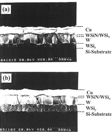
Figure 11 shows cross-sectional SEM micrographs for the ther-mally annealed Cu/WSiN/WSix/W(450 nm)/p1-n junction diodes. For the 7008C-annealed samples, a WSiylayer was formed between
the original W layer and the Si substrate (Fig. 11a), while the obser-vation with the naked eye on the Cu surface revealed no obvious change in coppery color. From the XRD spectra shown in Fig. 8b, we believe that the WSiylayer was WSi2phase. After annealing at
7508C, the WSiylayer become thicker, but Cu3Si precipitates were not observed (Fig. 11b).
Conclusion
The barrier capability of selective CVD-W(450 nm) films as well as WSiN/WSix(75 nm)/W(450 nm) stacked layers used as a
diffu-sion barrier between Cu and Si substrates against Cu diffudiffu-sion was investigated. We found that the CVD-W layers functioned as an effective barrier against Cu diffusion, and the Cu/W(450 nm)/p1-n junction diodes were able to sustain a 30 min furnace annealing up to 6508C without causing degradation in electrical characteristics. Thermal stability of the Cu/W/p1-n diodes can be significantly im-proved by inserting an N2-plasma-treated WSiN/WSix bilayer be-tween the W and Cu overlayers, and the Cu/WSiN/WSix/W/p1-n
junction diodes were able to retain their integrity in electrical
char-acteristics up to at least 7008C. Various evidences show that the thin WSiN layers formed by N2plasma treatment on the surfaces of WSix
layers efficiently suppressed Cu diffusion and thus resulted in im-provement of barrier capability. Failure of barrier capability for the W films was presumably due to interdiffusion of Cu and Si along grain boundaries of the W films, and the interdiffusion was probably enhanced by the formation of WSi2.
Acknowledgments
This work was supported by the National Science Council (ROC) under contact no. NSC87-2215-E-009-072.
National Chiao-Tung University assisted in meeting the publication costs of this article.
References
1. R. J. Gutmann, T. P. Chow, A. E. Kaloyeros, W. A. Lanford, and S. P. Murarka, Thin Solid Films, 262, 177 (1995).
2. N. Awaya, H. Inokawa, E. Yamamoto, Y. Okazaki, M. Miyake, Y. Arita, and T. Kobayashi, IEEE Trans. Electron Devices, ED-43, 1206 (1996).
3. V. M. Dubin and Y. S. Diamand, J. Electrochem. Soc., 144, 898 (1997). 4. J. C. Chiou, K. C. Juang, and M. C. Chen, J. Electrochem. Soc., 142, 177 (1995). 5. J. C. Chiou, Y. J. Chen, and M. C. Chen, J. Electron. Mater., 23, 383 (1994). 6. C. A. Chang, J. Appl. Phys., 67, 566 (1990).
7. S. H. Corn and J. L. Falconer, J. Vac. Sci. Technol., A6, 1012 (1988).
8. Y. Shacham-Diamand, A. Dedhia, D. Hoffstetter, and W. G. Oldham, J. Electro-chem. Soc., 140, 2427 (1993).
9. A. L. S. Loke, C. Ryu, C. P. Yue, J. S. H. Cho, and S. S. Wong, IEEE Electron De-vice Lett., EDL-17, 549 (1996).
10. J. C. Chiou, H. I. Wang, and M. C. Chen, J. Electrochem. Soc., 143, 990 (1996). 11. M-A. Nicolet, Thin Solid Films, 54, 415 (1978).
12. M. Wittmer, J. Vac. Sci. Technol., A2, 273 (1984).
13. H. Ono, T. Nakano, and T. Ohta, Appl. Phys. Lett., 64, 1511 (1994).
14. W. K. Yeh, T. T. Wu, M. H. Tsai, S. C. Sun, J. C. Chuang, and M. C. Chen, VMIC Proceedings, June 1996, p. 541.
15. S. D. Kim, S. G. Jin, M. R. Hong, and C. T. Kim, J. Electrochem. Soc., 144, 664 (1997).
16. S. Q. Wang, J. Appl. Phys., 73, 2301 (1993).
17. J. C. Chiou, K. C. Juang, and M. C. Chen, J. Electrochem. Soc., 142, 2326 (1995). 18. X. Sun, E. Kolawa, J. S. Chen, J. S. Reid, and M-A. Nicolet, Thin Solid Films, 236,
347 (1993).
19. K. Holloway and P. M. Fryer, Appl. Phys. Lett., 57, 1736 (1990).
20. K. Holloway, P. M. Fryer, C. Cabral, Jr., J. M. E. Harper, P. J. Bailey, and K. H. Kelleher, J. Appl. Phys., 71, 5433 (1992).
21. E. Kolawa, J. S. Chen, J. S. Reid, P. J. Pokela, and M-A. Nicolet, J. Appl. Phys., 70, 1369 (1991).
22. T. Oku, E. Kawakami, M. Uekubo, K. Takahiro, S. Yamaguchi, and M. Murakami, Appl. Surf. Sci., 99, 265 (1996).
23. M. Takeyama, A. Noya, T. Sase, and A. Ohta, J. Vac. Sci. Technol., B14, 674 (1996). 24. R. G. Schad, F. Cardone, and L. Stolt, J. Appl. Phys., 73, 301 (1993).
25. M. S. Angyal, Y. S. Diamand, J. S. Reid, and M-A. Nicolet, Appl. Phys. Lett., 67, 2152 (1995).
26. W. K. Yeh, K. Y. Chan, T. C. Chang, M. S. Lin, and M. C. Chen, J. Electrochem. Soc., 143, 2053 (1996).
27. M. T. Wang, M. S. Tsai, C. Liu, W. T. Tseng, T. C. Chang, L. J. Chen, and M. C. Chen, Mater. Chem. Phys., 51, 75 (1997).
28. B. W. Shen, G. C. Smith, J. M. Anthony, and R. Matyi, J. Vac. Sci. Technol., B4, 1369 (1986).
29. T. Hara, S. Enomoto, N. Ohtsuka, and S. Shima, Jpn. J. Appl. Phys., 24, 828 (1985). 30. M. T. Wang, P. C. Wang, L. J. Chen, and M. C. Chen, Unpublished.
31. M. T. Wang, Y. C. Lin, J. Y. Lee, C. C. Wang, and M. C. Chen, Unpublished. 32. M. T. Wang, Y. C. Lin, M. C. Chun, M. S. Chuang, L. J. Chen, and M. C. Chen,
Unpublished.
33. Y. Shimooka, T. Iijima, S. Nakamura, and K. Suguro, Jpn. J. Appl. Phys., 36, 1589 (1977).
34. A. Hirata, T. Hosoya, K. Machida, H. Takaoka, and H. Akiya, J. Electrochem. Soc.,
143, 3747 (1996).
35. S. P. Murarka, Silicides for VLSI Applications, pp. 128–131, Academic Press, New York (1983).
Figure 11. Cross-sectional view SEM micrographs for the Cu/WSiN/WSix/ W/p1-n junction diodes annealed at (a) 700 and (b) 7508C.