IEEE ELECTRON DEVICE LETTERS, VOL. 16, NO. 11, NOVEMBER 1995 SO3
The Effects of
NH3 Plasma Passivation
on Polysilicon Thin-Film Transistors
Fang-Shing Wang, Meng-Jin Tsai, and Huang-Chung Cheng,
Member, IEEEAbstract-The NH3 plasma passivation has been performed for the first time on the polycrystalline silicon (poly-Si) thin-film transistors (TFT's). It is found that the TFT's after the NH3 plasma passivation achieve better device performances, including the off-current below 0.1 pA/pm and the on/off current ratio higher than lo8, and also better hot-carrier reliability as well as
thermal stability than the Hz -plasma ones. These improvements were attributed to not only the hydrogen passivation of the grain-boundary dangling bonds, but also the nitrogen pile-up at SiOz/poly-Si interface and the strong Si-N bond formation to terminate the dangling bonds at the grain boundaries of the polysilicon films.
I. INTRODUCTION
OLYCRYSTALLINE silicon (Poly-Si) thin-film transis-
P
tors (TIT'S) are of interest for a number of applications, such as ultra-large-scale-integration (ULSI) memories and large-area electronic devices (displays, sensors, etc.) [ 11, [2]. In these devices, defects either in the bulk or at grain boundaries play a critical role [3]. To obtain high-performance poly- Si TFYs, it is necessary to reduce the trap-states of the polysilicon films. It is now well known that hydrogenation leads to tie up the grain boundary dangling bonds with hydrogen, thereby significantly improve the characteristics of the poly-Si TFT's [4]. However, it had been observed that the characteristics of the poly-Si TFT's after the hydrogen passivation suffer a low hot-carrier endurance and a low thermal stability [5], [6]. In this letter, a simpler technique, "3-plasma passivation, was employed to enhance both the electrical reliability and the thermal stability of the poly-SiT F T ' S .
11. EXPERIMENTAL PROCEDURES
The poly-Si TFT's were fabricated on thermally oxidized silicon wafers. A 110 nm thick amorphous silicon (a-Si) was initially deposited at 550°C by low-pressure chemical vapor deposition (LPCVD) using pure SiH4, and then furnace annealed at 600°C for 24 h in N2 ambient to recrystallize the silicon films. After defining the active islands, a 70 nm thick silicon-dioxide was thermally grown by dry oxidation. Another 300 nm polysilicon film was deposited at 6 2 0 T in an Manuscript received April 27, 1995; revised August 1, 1995. This work was supported in part by the Republic of China National Science Council under Contract NSC-79-0425-Em-013.
F.-S. Wang and H.-C. Cheng are with the Department of Electronics Engineering and Institute of Electronics, National Chiao Tung University, Hsinchu 300, Taiwan, R.O.C.
M.-J. Tsai is with the United Microelectronics Corporation, Hsinchu 300, Taiwan, R.O.C.
IEEE Log Number 9414969.
LPCVD system and patterned to be the gates of the devices. A self-aligned POC13 doping was performed at 900 "C for 20 min to form the source, drain, and gate electrodes. Then, the samples were subjected to the NH3 or H2 plasma treatment in a parallel-plate plasma reactor at 300°C with a power density of 0.7 W/cm2. The plasma conditions for NH3 and H2 had been optimized to obtain the optimum device performance, respectively. After a plasma-enhanced CVD (PECVD) Si02 of a thickness about
500
nm was deposited, contact holes were opened and the A1 films was deposited and then defined. The I-V curves of TIT'S were measured by an HP 4145 semiconductor parameter analyzer at room temperature. The concentration of the nitrogen atom was measured by detecting the Si-N signals using a secondary ion mass spectroscopy (SIMS) with Cs' as the primary ion.111. RESULTS AND DISCUSSION
The I d - Vg characteristics of the n-channel poly-Si TFT's with various NH3-plasma exposure times from 0 to 120 min are shown in Fig. 1. The transfer curves of the devices with a 30 min H2-plasma and without a plasma treatment are also shown for comparison. Table I lists the values of the minimum leakage current I m i n , the subthreshold swing SS, the odoff current ratio, the threshold voltage Vth, the field effect mobility FE, and the trap-state density N t . The S S and p p ~ were measured at v d = 0.1
v
forw/L
= 40 pm/10 pm devices. The Vth is defined at a fixed drain current I d = Id,, x W / L , for this work, where I d n is a normalized drain current, 10 nA [7]. The I m i n is the minimum value of the drain current measured at v d = 5 V. The Nt is obtained by extracting a straight line on the plot of l n [ I d / ( v g-
V&)] versus l/(Vg - V F B ) ~ at low source-drain voltage and high gate bias [8], [9]. It is obvious that the "3-plasma and H2-plasma treatment both can effectively promote the performance of the'IW's. In addition, it seems that the devices treated by "3- plasma for 30 min have even better performance than that treated by H2-plasma. Moreover, as the exposure time to "3- plasma increases, the TFT's performance can be enhanced increasingly, such as Imin and S S decreasing to 3.54 PA, and 200 mVIdecade and FE and ordoff current ratio increasing to 79.93 cm2Ns and 2.23 x lo8, respectively, for 120 min "3- plasma treated devices, unlike the earlier report that the TIT'S
exposed to H2-plasma exhibited saturation characteristics [lo]. The hot-carrier reliability of the "3-plasma-treated de- vices was also investigated. Fig. 2 shows the FE and I m i n variations for the devices with the NH3 and H2 plasma passivation, respectively, after they were stressed at v d = 20 0741-3106/95$04.00 0 1995 IEEE
504 IEEE ELECTRON DEVICE LE'ITERS, VOL. 16, NO. 11, NOVEMBER 1995 h W -4
2
U C 2 I.G
C.-
E
n
Fig. 1 plasma 10-2 c I lo4 lo4 10.' vd=sv -0- No plasma tnarment---o.-- m-plasma 3chnin.
-
"3-plasma 3ormn --a--NH3-plasnla60 min-
"3-plasma lzomin I I I I I -10 -5 0 5 10 15m
Gate Voltage (V)The transfer characteristics of polysilicon T I T S after applying NH3 treatments. 0 ) I.
e
B
e! a L a.
a
B 2 ld n W h 8 W 10' 10' 1 0'Stress time (sec)
Fig. 2. The field effect mobility FE and minimum drain current Imin for "3- and Hz-passivated devices as a function of stress time.
TABLE I
POLYSILICON Tm'S FOR VARIOUS PLASMA TREATMENTS THE VALUES OF Imin,
ss,
FE, t'ih, AND N t OF THEFlasmr The Li. ss wmaureat va N,
Gas (min) @A) (Vldec.) nfio(x106) 01) ( w%ec) (xlO"cm'2)
-
0 463.6 1.81 0.024 7.18 11.35 63.9 Hz 30 81.03 0.61 4.11 1.46 51.31 14.8 NH, 60 10.30 0.28 71.0 0.46 75.12 8.61 N& 30 39.50 0.34 14.2 0.72 59.92 13.9 " 3 I20 3.54 0.20 223 -0.02 79.93 5.66V, V, = 10 V for different stress durations. It is found that the FE decreases and I m i n increases with hot-carrier stress time, and the variations of the FE and Imin for "3- plasma-treated devices are less than those for Hz-plasma- treated samples. That is, the NH3-plasma passivated devices have better hot-carrier reliability than the H2-plasma ones. The performance degradation of both devices induced by hot carrier stress is thought to be due to the generation of poly- SVSiO2 acceptor-type interface states and the grain boundary states in the poly-si channel layer E519 [ I l l . The hot-carrier endurance of NH3-plasma Passivation is better than that of the H2-plasma passivation, suggesting that not only hydrogen films. From the SIMS analysis, it is found that nitrOgen atoms can even diffuse to the bottom of the channel region. It is
possible that weak Si-H bonds in POlY-si channel and at Poly- SVSiO2 interface had been replaced by strong Si-N bonds. It had been reported that with the nitrogen implantation in the poly-Si gate/SiO2/c-Si substrate MOS structure, a much smaller interface-state generation rate was obtained after high- fieldcurrent stress [12]. Momose et al. also showed that with the low concentration (< 1 atom
%)
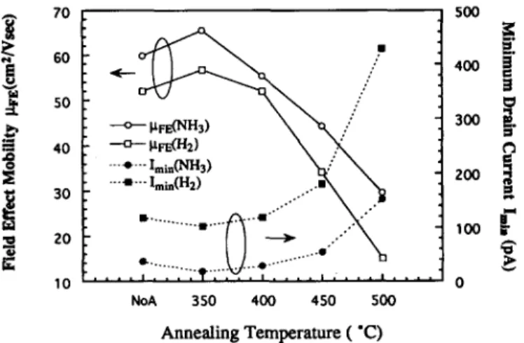
nitrogen incorporation inNoA 350 400 450 500
Annealing Temperature ( 'C)
Fig, 3. The variation of field effect mobility p F E and minimum drain current Imin for "3- and Hz-passivated devices after thermal annealing
at the temperature range from 3000c to 500 OC.
temperature continuously increases, the increase in Imin and decrease in p F E is attributed to the dehydrogenation effect since the hydrogen releases from the defect sites and causes the generation of trap states. But for the ",-treated W'S,
respect to the H 2-plasma ones. Even for 500°C annealing, the
m y s performance passivated with NH3-plasma still keeps
the relatively good electrical properties. Therefore, it suggests that the strong Si-N bonds exist in "3-passivated films and achieve superior thermal stability to weaker S ~ - H bonds. atoms but also nitrogen atoms are diffusing into the PolY-si lower degrees of p F E and Imin degradations are observed with
IV. CONCLUSIONS
the NH3 rapid thermal nitrided-oxide, both drivabiky and hot carrier reliability of MOSFET could be improved [13].
Fig. 3 shows the FE and Imin after thermal annealing for different annealing temperatures range from 350°C to 500°C. For the 350°C annealed devices, there is a slightly increase in / J F E and a slightly decrease in I m i n . This is presumably because of the annihilation of plasma induced damages and/or hydrogen and nitrogen atoms indiffusion, leading to a further passivation effect. As the annealing
The "3-plasma passivation has been used to promote the electrical properties of poly-Si TFT's. It is found that the poly-Si TFT's after NH3 plasma passivation exhibit signif- icantly superior device characteristics, hot-carrier reliability, and thermal stability to those with the conventional H2-plasma passivation. Both the nitrogen pile-up at the SiOz/poly-Si interface and the strong Si-N bond formation to passivate the dangling bonds at the grain boundaries in the channel region are surmised to be the major causes.
WANG et al.: EFFECTS OF NH3 PLASMA PASSIVATION ON TFT’s
ACKNOWLEDGMENT
The authors thank the National Nan0 Device Laboratory and the Semiconductor Research Center at National Chiao Tung University for their technical support.
REFERENCES
W. G. Hawkins, “Polycrystalline-silicon devices technology for large-
area electronics,” IEEE Trans. Electron Devices, vol. ED-33, pp. 477-48 1, 1986.
P. Migliorato and D. B. Meakin, “Material properties and characteristics of polysilicon transistors for large area electronics,” Appl. SUI$ Sci., vol. 30, p. 353, 1987.
K. Ono, T. Anoyama, N. Konishi, and K. Miyata, “Analysis of current- voltage characteristics of low-temperature-processed polysilicon thin film transistors,” IEEE Trans. Electron Devices, vol. 39, pp. 792-802, 1992.
B. A. Khan and R. Pandya, “Activation-energy of source-drain current in hydrogenated and unhydrogenated polysilicon thin-films transistors,”
IEEE Trans. Electron Devices, vol. 37, pp. 1727-1734, 1990.
S. Banerjee, R. Sundaresan, H. Schichijo, and S. Malhi, “Hot-carrier
degradation of n-channel polysilicon MOSFET’s,” IEEE Trans. Electron
Devices, vol. 35, pp. 152-157, 1988.
505
M. Hack, A. G. Lewis, and I-W. Wu, “Physical models for degrada- tion effects in polysilicon thin-film transistors,” IEEE Trans. Electron
Devices, vol. 40, pp. 8 W 8 9 7 , 1993.
A. G. Lewis, T. Y. Huang, R. H. Bruce, M. Koyanagi, A. Chiang and I-W. Wu, “Polysilicon thin film transistors for analogue circuit applications,” in ZEDM Tech. Dig., pp. 264-267, 1988.
J. Levinson, F. R. Shepherd, P. J. Scanlon, W. D. Westwood, G. Este, and M. Rider, “Conductivity behavior in polycrystalline semiconductor thin film transistors,” J. Appl. Phys., vol. 53, pp. 1193-1202, 1982. R. E. Proano, R. S. Misage, and D. G. Ast, “Development and electrical properties of undoped polycrystalline silicon thin-film transistors,” IEEE
Trans. Electron Devices, vol. 36, pp. 1915-1922, 1989.
H. N. Chern, C. L. Lee, and T. F. Lei, “The effects of HZ - 0 2 -plasma
treatment on the characteristics of polysilicon thin film transistors,”
IEEE Trans. Electron Devices, vol. 40, pp. 2301-2306, 1993. G. Fortunato, A. Pecora, G. Tallarida, L. Mariucci, C. Reita, and P. Migliorato, “Hot carrier effects in n-channel polycrystalline silicon thin- film transistors: a correlation between off-current and transconductance variations,” IEEE Trans. Electron Devices, vol. 41, pp. 34C346, 1994.
S. Haddad and M. S. Liang, “Improvement of thin-gate oxide integrity
using through-silicon-gate nitrogen ion implantation,” ZEEE Electron
Device Lett., vol. EDL-8, pp. 58-60, 1987.
H. S. Momose, T. Morimoto, Y. Ozawa, K. Yamabe, and H. Iwai, “Electrical characteristics of rapid thermal nitrided-oxide gate n- and p-MOSFET’s with less than 1% atom nitrogen concentration,” IEEE