IEEE ELECTRON DEVICE LETTERS, VOL. 28, NO. 7, JULY 2007 599
High-Performance Self-Aligned
Bottom-Gate Low-Temperature Poly-Silicon
Thin-Film Transistors With Excimer
Laser Crystallization
Chun-Chien Tsai, Hsu-Hsin Chen, Bo-Ting Chen, and Huang-Chung Cheng
Abstract—In this letter, high-performance bottom-gate (BG) low-temperature poly-silicon thin-film transistors (TFTs) with excimer laser crystallization have been demonstrated using self-aligned (SA) backside photolithography exposure. The grains with lateral grain size of about 0.75µm could be artificially grown in the channel region via the super-lateral-growth phenomenon fab-ricated by excimer laser irradiation. Consequently, SA-BG TFTs with the channel length of 1 µm exhibited field-effect mobility reaching 193 cm2/V · s without hydrogenation, while the mobility of the conventional non-SA-BG TFT and conventional SA top-gate one were about 17.8 and 103 cm2/V · s, respectively. Moreover, SA-BG TFTs showed higher device uniformity and wider process window owing to the homogenous lateral grains crystallized from the channel steps near the BG edges.
Index Terms—Bottom gate (BG), excimer laser crystalliza-tion (ELC), lateral grain growth, self-aligned (SA), thin-film transistor (TFT).
I. INTRODUCTION
L
OW-TEMPERATURE poly-silicon (LTPS) thin-film tran-sistors (TFTs) have been extensively investigated for use in matrix liquid-crystal displays (AMLCDs) and active-matrix organic light-emitting displays [1], [2]. The mobility of poly-Si TFTs fabricated by excimer laser crystallization (ELC) is generally two orders higher than amorphous-Si (a-Si) TFTs; therefore, the peripheral driving circuits and pixel elements can be integrated on the same glass substrate. In the early stage of the LTPS TFTs development, bottom-gate (BG) TFT structure was attractive because the ELC was thought as an additional process step to the a-Si TFTs. However, BG TFTs suffered from worse electrical performance than top-gate (TG) TFTs because of the smaller grain size and poor grain quality resulting from the BG metal acting as a heat sink during ELC [3], [4]. Moreover, BG TFTs exhibited significant performanceManuscript received April 5, 2007; revised April 23, 2007. This work was supported in part by the National Science Council of Taiwan, R.O.C., under Contract NSC 94-2218-E-009-027 and in part by the Nano Facility Center of National Chiao Tung University and National Nano Device Laboratories for providing process equipment. The review of this letter was arranged by Editor J. Sin.
The authors are with the Department of Electronics Engineering and Institute of Electronics, National Chiao Tung University, Hsinchu 300, Taiwan, R.O.C. (e-mail: [email protected]).
Color versions of one or more of the figures in this letter are available online at http://ieeexplore.ieee.org.
Digital Object Identifier 10.1109/LED.2007.899326
variation as the devices scaled-down owing to the misalignment effect. Although some self-aligned (SA) BG TFTs have been demonstrated, the device processes were too complicated to be utilized in the large-area fabrication [5], [6]. As a result, only a few studies have been conducted for BG TFTs with short channel length, and TG TFTs have been widely adopted in AMLCDs due to the self-alignment capability in the last decade. Although high field-effect mobility for TG-TFTs has been attained by ELC, it is difficult to make the laser-energy density hit the super-lateral-growth (SLG) regime everywhere due to the narrow laser process window [7]–[9]. Consequently, poor device uniformity and narrow process window were en-countered in TG-TFTs. Furthermore, in the applications of system-on-panel, TFTs must exhibit good uniformity of device performance. Thus, many laser-crystallization methods were proposed to solve the above problems [10]–[17]. However, most of them need complex fabrication process or are problematic for circuit layout due to the anisotropy of the grain-boundary spacing.
In this letter, an SA-BG TFT with appropriate channel length has been fabricated by the simple ELC and backside exposure. The process steps in these technologies are not only highly compatible with the conventional commercial a-Si TFT process but also with minimum parasitic capacitance for high circuit performance. Owing to the lateral grain growth and SA structure, SA-BG TFTs exhibit higher performance and better uniformity.
II. DEVICEFABRICATION
Fig. 1 illustrates the key processes for the fabrication of SA-BG LTPS TFTs and non-SA-BG ones. At first, a 1000-Å-thick phosphorus-doped a-Si layer was deposited by LPCVD at 550 ◦C on quartz wafer. After defining the BG region, a 1000-Å-thick tetraethyl orthosilicate gate oxide layer was de-posited by PECVD at 385 ◦C and a 1000-Å-thick a-Si layer was subsequently deposited by LPCVD at 550◦C. The samples were performed by KrF ELC(λ = 248 nm) at room temper-ature in a vacuum chamber of 10−3 torr. The number of laser shots per area was 20 (i.e., 95% overlapping), and the laser-energy density was varied. A SA photolithography, using the BG as an opaque mask, was applied by backside exposure through the quartz substrate [18], [19], while for the non-SA
600 IEEE ELECTRON DEVICE LETTERS, VOL. 28, NO. 7, JULY 2007
Fig. 1. Key-process procedures for fabricating small-dimension SA BG LTPS TFTs with lateral grain growth and the non-SA BG ones.
TFT, a front-side UV light exposure is used in defining the source/drain regions which result in the offset region. The offset length in non-SA TFT is about 0.45µm due to the process of masker aligner, and the offset length can be further reduced by using the I-line stepper system. It is worth mentioning that the fabrication processes of new SA TFTs and conventional non-SA ones are almost the same, except the lithography process of defining the source/drain regions. Then, a phosphorous ion implantation with a dose of 5× 1015 cm−2 was carried out to form source-and-drain regions followed by the definition of active region by reactive-ion-etching. Next, the typical passiva-tion layer deposipassiva-tion, dopants activapassiva-tion, contact holes opening, and metallization completed the fabrication of SA-BG TFTs. No hydrogenation plasma treatment was performed during the device-fabrication process. For comparison, the conventional non-SA-BG TFTs were also fabricated. In addition, for clari-fying the effect of poly-Si grain structures on electrical charac-teristics, conventional SA-TG TFTs were also fabricated using the SLG laser-annealing condition.
III. RESULTS ANDDISCUSSION
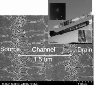
Fig. 2 displays the SEM photograph of ELC poly-Si films with BG structure after Secco etching and the length of BG is 1.5 µm. It can be observed that the grains with 0.75 µm
Fig. 2. SEM micrograph of ELC poly-Si film with BG structure after Secco etching. The inset of Fig. 2 is the cross-sectional TEM image and the diffraction pattern of laser-crystallized poly-Si thin films of BG devices.
in lateral dimension were formed in the channel region, while small and fine grains were located near the edges of the BG. For the short channel length with the proper thicknesses of gate
TSAI et al.: HIGH-PERFORMANCE SELF-ALIGNED BG LOW-TEMPERATURE POLY-SILICON TFTs WITH ELC 601
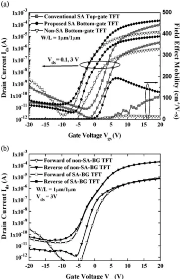
Fig. 3. (a)I–V curves of SA-BG TFT with lateral silicon grain, non-SA-BG TFT, and conventional TG TFT. (b) Experimental measured bidirectional trans-fer characteristics of SA-BG TFT and non-SA-BG TFT under the polarities of the source and drain are interchanged.
electrode, gate oxide, and channel layers using this crystalliza-tion, only single-grain boundary perpendicular to the channel direction is also observed by TEM image, shown in the inset of Fig. 2. It has been reported that lateral thermal gradient could arise from the heat generated at moving solid–melt interfaces [9], [20]. In this experiment, as a proper excimer laser irradi-ation was performed on the a-Si thin film with BG structure, the laser-energy densities could cause complete melting of 1000-Å-thick silicon thin film in the channel region but partial melting of the thicker a-Si film near the edges of the BG. Therefore, the lateral grain growth started from the unmelted silicon solid seeds near the BG corner and extended toward the completely melted region until the solid–melt interface from opposite direction impinged. If the channel region, i.e., BG plateau, were arranged in a proper distance, there were two columns of longitudinal grains colliding in the middle of the channel region without any spontaneous nucleation. Thus, the grain boundaries in the channel region could be controlled and reduced. Moreover, the process window could be broaden because the laser-energy densities, between completely melting silicon thin film in the channel but partially melting the thicker
TABLE I
MEASUREDELECTRICALCHARACTERISTICS OFSA-BG TFTSWITH LATERALGRAINGROWTH ANDCONVENTIONALONES. THETHRESHOLD VOLTAGEWASDEFINED AS THEGATEVOLTAGEREQUIRED TOACHIEVE
ANORMALIZEDDRAINCURRENT OFIds= (W/L) × 10−8A ATVds= 0.1 V. THEFIELD-EFFECTMOBILITY AND
SUBTHRESHOLDSWINGWEREEXTRACTED AT Vds= 0.1 V,AND THEION/IOFFCURRENT
RATIOWASDEFINED ATVds= 3 V
one at the corner, were easier to be controlled for the wider range from 430 to 510 mJ/cm2.
Typical transfer characteristics of SA-BG TFTs, conven-tional non-SA-BG TFTs, and SA-TG ones forW = L = 1 µm are shown in Fig. 3(a). Table I lists the average values of several important electrical characteristics of these three different TFTs. Owing to the uniformly large transverse grains grown in the channel region and SA source/drain to the BG, this proposed SA-BG TFTs exhibited better electrical characteristics with field-effect-mobility of 193 cm2/V · s. Although the poly-Si grain structure in the channel region is similar in the SA-BG and non-SA-BG TFTs after ELC. However, after the lithography process of defining the source/drain regions, the lateral grain structure is still symmetric above the gate electrode in the SA TFTs, while the grain structure becomes asymmetric in the channel region, and there is an offset region in the conventional non-SA TFTs due to the misaligment process effect. In consequence, for the non-SA TFTs, because small and fine grains are near the edges of BG and the series resistance of the offset region is large, the non-SA-BG TFTs display lower field-effect mobility, and lower on-current [21]. Fig. 3(b) shows the transfer characteristics of SA-BG TFTs and non-SA-BG ones under both the forward- and reverse-measurement modes. The symmetric electrical characteristics confirmed that the proposed TFT is a SA gate structure. Moreover, to study the uniformity of these three different TFTs performance, 20 TFTs for the optimal laser-irradiation condition are measured. SA-TG TFTs display the worst uniformity which the mobilities range from 45 to 285 cm2/V · s owing to the nonuniform grain distribution in the SLG regime. As for the BG devices, the mobilities of the SA-BG TFTs range from 170 to 210 cm2/V · s, but for the non-SA BG-TFTs, the mobilities range from 8.5 to 60 cm2/V · s. It is found that the variation range of mobility is similar about 50 cm2/V · s. But for the calculation of nonuniformity, our definition of nonuniformity is (maximum mobility − minimum mobility)/(average mobility). As a result, the non-uniformity of non-SA-BG device is worse from the lower average mobility. The standard deviation of field-effect
602 IEEE ELECTRON DEVICE LETTERS, VOL. 28, NO. 7, JULY 2007
mobility for these three different TFTs is listed in Table I. It could be concluded that SA-BG TFTs exhibit better characteristics and improved uniformity based on the lateral grain growth and SA structure.
IV. CONCLUSION
High-performance SA-BG LTPS TFTs have been fabricated by ELC with backside exposure. Consequently, besides the high field-effect mobility, symmetric electrical characteristics and good device uniformity are achieved owing to the arti-ficially controlled lateral grains with SA structure. The SA-BG TFTs are, therefore, promising for future system-on-panel applications.
REFERENCES
[1] H. J. Kim, D. Kim, J. H. Lee, I. G. Kim, G. S. Moon, J. H. Huh, J. W. Hwang, S. Y. Joo, K. W. Kim, and J. H. Souk, “A 7-in. full-color low-temperature poly-Si TFT-LCD,” in Proc. SID Tech. Dig., 1999, pp. 184–187.
[2] Y. I. Park, T. J. Ahn, S. K. Kim, J. Y. Park, J. S. Yoo, C. Y. Kim, and C. D. Kim, “Active matrix OLED displays using simple Poly-Si TFT process,” in Proc. SID Tech. Dig., 2003, pp. 487–489.
[3] Y. Mishima, K. Yoshino, M. Takei, and N. Sasaki, “Characteristics of low-temperature poly-Si TFTs on Al/Glass substrates,” IEEE Trans. Electron Devices, vol. 48, no. 6, pp. 1087–1091, Jun. 2001.
[4] I. W. Wu, “Polycrystalline silicon thin film transistors for liquid crystal displays,” Solid State Phenom., vol. 37/38, pp. 553–564, 1994. [Online]. Available: http://www.scientific.net
[5] S. Zhang, R. Han, Z. Zhang, R. Huang, P. K. Ko, and M. Chan, “Implementation of fully self-aligned bottom-gate MOS transistor,” IEEE Electron Device Lett., vol. 23, no. 10, pp. 618–620, Oct. 2002. [6] R. S. Shenoy and K. C. Saraswat, “Novel process for fully self-aligned
planar ultrathin body double-gate FET,” in Proc. IEEE Int. SOI Conf., 2004, pp. 190–191.
[7] A. Hara, F. Takeuchi, and N. Sasaki, “Mobility enhancement limit of excimer-laser-crystallized polycrystalline silicon thin film transistors,” J. Appl. Phys., vol. 91, no. 2, pp. 708–714, Jan. 2002.
[8] J. S. Im, H. J. Kim, and M. O. Thompson, “Phase transformation mech-anisms involved on excimer laser crystallization of amorphous silicon films,” Appl. Phys. Lett., vol. 63, no. 14, pp. 1969–1971, Oct. 1993. [9] J. S. Im and H. J. Kim, “On the super lateral growth phenomenon observed
in excimer laser-induced crystallization of thin Si films,” Appl. Phys. Lett., vol. 64, no. 17, pp. 2303–2305, Apr. 1994.
[10] M. A. Crowder, P. G. Carey, P. M. Smith, R. S. Sposili, H. S. Cho, and J. S. Im, “Low-temperature single-crystal Si TFT’s fabricated on Si films processed via sequential lateral solidification,” IEEE Electron Device Lett., vol. 19, no. 8, pp. 306–308, Aug. 1998.
[11] P. C. van der Wilt, B. D. van Dijk, G. J. Bertens, R. Ishihara, and C. I. M. Beenakker, “Formation of location-controlled crystalline is-lands using substrate-embedded seeds in excimer-laser crystallization of silicon films,” Appl. Phys. Lett., vol. 79, no. 12, pp. 1819–1821, Sep. 2001.
[12] L. Mariucci, R. Carluccio, A. Pecora, V. Foglietti, G. Fortunato, P. Legagneux, D. Pribat, D. Della Sala, and J. Stoemenos, “Lateral growth control in excimer laser crystallized polysilicon,” Thin Solid Films, vol. 337, no. 1/2, pp. 137–142, Jan. 1999.
[13] R. Ishihara, A. Burtsev, and P. F. A. Alkemade, “Location-control of large Si grains by dual-beam excimer-laser and thick oxide portion,” Jpn. J. Appl. Phys. 1, Regul. Rap. Short Notes, vol. 39, no. 7A, pp. 3872–3878, Jul. 2000.
[14] S. Sakuragi, T. Kudo, K. Yamazaki, and T. Asano, “High field effect mo-bility poly-Si TFTs fabricated by advanced lateral crystal growth process using double-pulsed laser annealing system,” in Proc. 12th Int. Display Workshops, 2005, pp. 965–968.
[15] C. H. Kim, I. H. Song, W. J. Nam, and M. K. Han, “A poly-Si TFT fabricated by excimer laser recrystallization on floating active structure,” IEEE Electron Device Lett., vol. 23, no. 6, pp. 315–317, Jun. 2002.
[16] A. Hara, M. Takei, F. Takeuchi, K. Suga, K. Yoshino, M. Chida, T. Kakehi, Y. Ebiko, Y. Sano, and N. Sasaki, “High performance low temperature polycrystalline silicon thin film transistors on non-alkaline glass produced using diode pumped solid state continuous wave laser lateral crystalliza-tion,” Jpn. J. Appl. Phys. 1, Regul. Rap. Short Notes, vol. 43, no. 4A, pp. 1269–1276, 2004.
[17] M. Tai, M. Hatano, S. Yamaguchi, T. Noda, S. K. Park, T. Shiba, and M. Ohkura, “Performance of poly-Si TFTs fabricated by SELAX,” IEEE Trans. Electron Devices, vol. 51, no. 6, pp. 934–939, Jun. 2004.
[18] Y. Kuo, “A self-aligned, tri-layer, a-Si:H thin film transistor prepared from two photo masks,” J. Electrochem. Soc., vol. 139, no. 4, pp. 1199–1204, 1992.
[19] Z. Xiong, H. Liu, C. Zhu, and J. K. O. Sin, “A new polysilicon CMOS self-aligned double-gate TFT technology,” IEEE Trans. Electron Devices, vol. 52, no. 12, pp. 2629–2633, Dec. 2005.
[20] M. H. Lee, S. J. Moon, M. Hatano, K. Suzuki, and C. P. Grigoropoulos, “Relationship between fluence gradient and lateral grain growth in spatially controlled excimer laser crystallization of amor-phous silicon films,” J. Appl. Phys., vol. 88, no. 9, pp. 4994–4999, Nov. 2000.
[21] R. Ishihara, “Effects of grain-boundaries on excimer-laser crystal-lized poly-Si thin-film transistors,” in Proc. AMLCD Tech. Dig., 2001, pp. 259–260.