The Influences of Contact Interfaces Between the Indium Tin
Oxide-Based Contact Layer and GaN-Based LEDs
Chin-Yuan Hsu,aWen-How Lan,b,zand YewChung Sermon Wua
a
Department of Materials Science and Engineering, National Chiao Tung University, Hsinchu 300, Taiwan b
Department of Electrical Engineering, National University of Kaohsiung, Kaohsiung 811, Taiwan
We have fabricated GaN-based light-emitting diodes共LEDs兲 using transparent indium tin oxide-based 共ITO-based兲 p contacts. The current-voltage characteristics and life tests of GaN-based LEDs have been studied. LED life tests showed that a pure ITO contact layer had poor reliability at high current stress. We also found that the GaN-based LED could achieve good reliability with a NiO/ITO contact layer. Using transmission electron microscopy and energy-dispersive X-ray spectrometer analyses, we observed In-contained metallic interface between the p-GaN layer and the pure ITO contact layer after annealing at 600°C. It revealed that ITO would react at interface or indiffuse near the interface at 600°C. The LED was degraded with unstable interfaces after life tests 共stressed by a 50-mA current injection兲. To improve the reliability of GaN-based LEDs with the ITO contact layer, we suggest that the NiO layer be used to prevent the reaction and block the leakage pathway.
© 2006 The Electrochemical Society. 关DOI: 10.1149/1.2184071兴 All rights reserved.
Manuscript submitted June 3, 2005; revised manuscript received November 25, 2005. Available electronically March 27, 2006.
GaN-based light emitting diodes共LEDs兲 operating in the green-to-violet range of the visible spectrum are commercially available and have received much attention. One of the problems in GaN-based devices is the low hole concentration of Mg-doped GaN, which makes it difficult to obtain contact resistance lower than 10−4⍀ cm2. In order to ohmic contact on p-type GaN, high work
function metals such as Ni, Pd, and Pt were applied. The specific contact resistance around 10−2–10−6⍀ cm2can be achieved in the
Ni/Au, Pd/Au, Ni/Pt/Au, Pd/Pt/Au, and Ni/Pd/Au series.1-4Among these contacts, the Ni/Au bilayer contact is commonly used as a transparent ohmic contact on p-type GaN due to its low contact resistivity and high transparency.5
A high-brightness GaN-based LED is also an interesting issue because of its important role in full-color display and lighting appli-cations. To enhance the output intensity of GaN-base LEDs, it is necessary to reduce the contact resistance and to enhance the trans-mission efficiency of the upper transparent contact layer 共TCL兲. However, the transmittance of such a conventional Ni/Au contact is only around 60–80% in the 450–550-nm wavelengths. One possible way to solve this problem is to employ transparent indium tin oxide 共ITO兲, instead of Ni/Au, as the p-contact material. ITO is a well-known transparent conducting material with resistivity in the low 10−4⍀ cm range and with transmittance higher than 90% in the
blue wavelength region at optimized conditions.6 In fact, ITO has already been used in ZnSe7 and AlInGaP-based8 LEDs as the current-spreading layer and in AlInGaAs vertical cavity lasers 共VC-SEL兲 as an interactivity contact.9,10Recently, several studies have discussed the applications of the ITO contact layer to GaN-based LEDs.11-15 Margalith et al. reported the ITO contacted with p-type GaN, but exhibited a higher operating forward voltage for practical LEDs.11 Horng et al. pointed out that Ni–ITO could form good ohmic contact on p-GaN with annealing at 600°C in air.12
However, for high-power applications such as projectors and flash lamps, high-power GaN-based LEDs with an ITO p-type con-tact layer have been studied.15 Since power dissipation across the p-GaN/metal interface generated Joule heat, failure of LEDs and laser diodes共LDs兲 was due to indiffusion of the ohmic contact ele-ments along dislocations in the GaN epi layers, leading to an elec-trical short of the p-n junction.16,17Thus, it is essential to understand the thermal stability and metallurgy of ITO–GaN contact in addition to developing a low-resistance ohmic system.
In this work, the current-voltage I-V properties of GaN-based LEDs with different TCL共ITO-based兲 conditions have been studied. The surface morphology change has been characterized by scanning electron microscopy共SEM兲 and X-ray diffraction 共XRD兲 analysis.
We also discuss the life tests of these LED samples at high current stress, such as leakage current and light output variation. Transmis-sion electron microscopy共TEM兲 and energy-dispersive X-ray spec-trometer共EDS兲 studies have been used to observe the interface be-tween TCL and p-type GaN. This study can clearly characterize the influences of the thermal stability of metal contact layers on GaN-based LEDs compared with the electrical properties and life tests.
Experimental
The blue GaN-based multiple quantum well共MQW兲 LED wafers were grown by metallorganic chemical vapor deposition共MOCVD兲 on c-plane sapphire substrate. Trimethylgallium共TMGa兲, trimeth-ylindium共TMIn兲, and ammonia 共NH3兲 were used as Ga, In, and N
precursors, respectively. The layer structure consists of a GaN buffer layer, followed by a 1.5-m undoped GaN layer, a 3-m Si-共n兲 doped GaN layer 共n ⬇ 1 ⫻ 1018cm−3兲, the active layer, a 0.12-m-thick Mg-共p兲 doped AlGaN cladding layer 共p ⬇ 5 ⫻ 1017cm−3兲, and a Mg-共p兲 doped GaN contact layer 共p ⬃ 7
⫻ 1017cm−3兲. The active region, consisting of seven 5-nm/15-nm
InGaN/GaN quantum wells, is embedded in the region between p-type and n-type layers.
The LEDs were fabricated using standard lithography. In the first process step, a mesa was defined with standard photolithography and etched down into the n-type region by inductively coupled plasma reactive ion etching 共ICP-RIE兲 technology. The TCL was deposited by E-beam evaporation and defined on the p-GaN region. Table I gives the various TCL conditions of the samples. The Ni/Au 共4/3.5 nm兲 and Ni 共4 nm兲 on LED-C and -D were preannealed at 550°C in air for 15 min, respectively. Then, ITO film共250 nm兲 was deposited by E-beam evaporation at 300°C in O2atmosphere, fol-lowed by the annealing process at 600°C in air for 15 min. For n-type GaN, low-resistance ohmic contacts around 10−5–10−8⍀ cm2 range have been obtained using Ti/Al metals series.18The Ti/Al/Ti/Au共10 nm:400 nm/150 nm/800 nm兲 metals for the n-contact and bonding pad were then deposited with E-beam
z
E-mail: [email protected]
Table I. Various TCL conditions of the LED samples.
LED
sample TCL condition
LED-A Ni/Au共4/3.5 nm兲 → annealed at 600°C in air for 15 min LED-B ITO共250 nm兲 → annealed at 600°C in air for 15 min LED-C Ni/Au共4/3.5 nm兲 preannealed at 550°C in air for 15 min+
ITO共250 nm兲 → annealed at 600°C in air for 15 min LED-D Ni共4 nm兲 preannealed at 550°C in air for 15 min + ITO共250 nm兲
→annealed at 600°C in air for 15 min Journal of The Electrochemical Society, 153共5兲 G475-G478 共2006兲
0013-4651/2006/153共5兲/G475/4/$20.00 © The Electrochemical Society G475
) unless CC License in place (see abstract). ecsdl.org/site/terms_use
address. Redistribution subject to ECS terms of use (see 140.113.38.11
evaporation, followed by the annealing process at 300°C with con-tinuous nitrogen flow for 5 min. All the annealing processes were performed in a furnace.
The wafers were then cut into chips, which were packaged onto a transverse optical共TO兲 can. During the life testing, these chips with TO-can form were stressed by a 50-mA current injection at 25°C and a relative humidity of 40%. The electrical characteristics were measured at room temperature with a HP-4155 I-V analyzer. The SEM surface images were taken with a Hitachi S-4000 instru-ment. For TEM measurements, the specimens were carried out by JEOL JEM-2010 microscope operated at 200 kV.
Results and Discussion
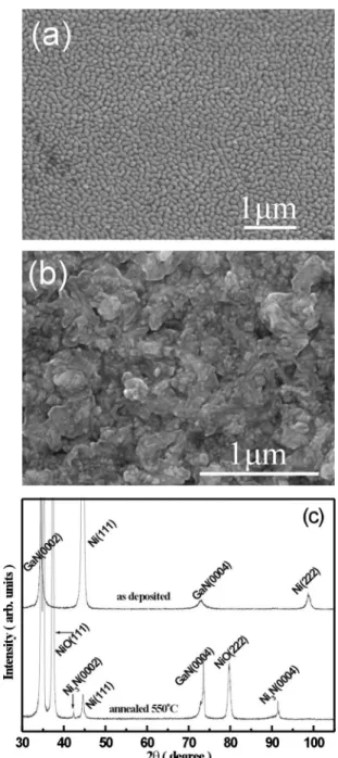
The I-V characteristics of the GaN-based LEDs with various TCL conditions are plotted on a semilogarithmic scale in Fig. 1. In the forward bias region, similar I-V characteristics with the ideality factor共n兲 around 3.0 can be seen under different TCL conditions. The ideality factors observed are 3.0 for LED-A, 3.3 for LED-B/C, and 3.6 for LED-D. This indicates that the injected carrier recombi-nation current in the space-charge region is a major mechanism of the current transport.19 For comparison, the dotted line shows a slope with the ideality factor n = 3 for room temperature. Thus, similar electron-hole recombination behavior can be expected in these LEDs. From I-V curves, the LEDs 共A, B, and C兲 showed almost the same operating voltage of 3.2 V at a forward current of 20 mA. In the LED-D curve, an increase of the parasitic series re-sistance and higher operating voltage共approximated 3.6 V兲 was ob-tained, which can be attributed to degradation of the TCL ohmic contact on top of the p-type GaN. Figure 2 shows the SEM images and XRD spectra of Ni film on the GaN surface. From Fig. 2a and b, the different surface morphology between as-deposited Ni film and after annealing at 550°C in air can be observed. According to Fig. 2c, the surface morphology change was mainly due to the Ni film being transformed to NiO. This reveals that the TCL of LED-D consisted of a NiO/ITO bilayer, and Ni film preannealed at 550°C in air is transformed to NiO, resulting in increasing contact resistance. In the reverse bias region, the leakage currents共⬍1 A兲 at −5 V were slightly different with various TCL conditions.
Figures 3 and 4 show the results of reliability tests by stress at 50 mA and 25°C, conducted on LEDs of the four types shown in Table I. The life tests of reverse leakage current共at −5 V兲, as shown in Fig. 3, showed that initial leakage currents observed from these LEDs were about the same, consistent with Fig. 1. It was also found that leakage current increased rapidly after 168 h for LED-B. Small increases of leakage currents for LED-A and LED-C were obtained after life tests. In contrast, a slight increase in leakage current could be found from LED-D even with an 840-h burn-in test. In Fig. 4, the life tests of light output variation共at 50 mA兲 were consistent with
the life tests of reverse leakage current. It could be observed that the optical output power was deteriorated by 10.8% for LED-B. Figures 3 and 4 show that GaN-based LEDs with ITO upper contact were unreliable after a longer burn-in test共stressed by 50 mA兲. Compared with only an ITO contact layer共LED-B兲, the NiO/ITO contact layer 共LED-D兲 was stable even with an 840-h burn-in test. These results are probably due to the NiO barrier layer that blocks the leakage pathway. Recently, Weidemann et al. have demonstrated that prefer-ential oxidation of threading dislocations共TDs兲 causes selective pas-sivation of leakage current paths.20Thus, the NiO thin film in this case may prevent metal indiffusion along defects or dislocations.
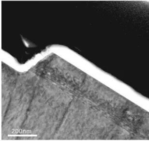
To further understand and confirm the influences of the contact interfaces between contact layers and the p-type GaN layer, we car-ried out TEM and EDS studies. Figure 5 shows the cross-sectional micrograph of the LED structure before coating contact metal 共TCL兲. The straight TDs were definitely seen in the LED structure. Figure 1. I-V characteristics of GaN-based LEDs with various TCL
condi-tions.
Figure 2. SEM images and XRD spectra of Ni film on GaN surface:共a兲
surface morphology of as-deposited Ni film on GaN,共b兲 after annealing at 550°C in air for 15 min, and共c兲 XRD spectra of as-deposited Ni film and after annealing.
G476 Journal of The Electrochemical Society, 153共5兲 G475-G478 共2006兲
G476
) unless CC License in place (see abstract). ecsdl.org/site/terms_use
address. Redistribution subject to ECS terms of use (see 140.113.38.11
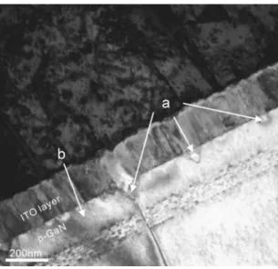
It was observed clearly that the upper p-GaN layer was flat and intact. In the image of the LED-B structure as shown in Fig. 6, ITO film contact on the p-GaN layer was obviously exhibited. In contrast with Fig. 5, the interface geometry changed substantially when it was annealed at 600°C. Numerous nanoscale dark points formed in the GaN just under the interface. It appears that the interface be-tween the ITO layer and p-GaN had been transformed after anneal-ing at 600°C. Under higher magnification, as shown in Fig. 7, the interface should be observed more clearly. The chemical composi-tions of the exposed regions, marked as “a” in Fig. 7, were analyzed by EDS. The Ga, In, and Sn peaks were detected as shown in Fig. 8a. In the p-GaN layer, marked as “b” in Fig. 7, only the Ga peak was observed, as shown in Fig. 8b. The Au and Cu signals are the background and copper ring, respectively. According to the results of EDS analyses, it is clearly indicated that ITO can react with p-GaN not only at TD 共or V-defects兲 interfaces but also at other interfacial regions. A similar phenomenon in interfacial reactions of Ti/n-GaN contacts at elevated temperature has been reported. 21 According to the above-mentioned results, we suggest that the ITO layer can react with the p-GaN layer to easily form an In–Ga solid solution near the interface due to the lower eutectic temperature 共15.3°C兲 of the Ga–In phase system. In contrast, Ni film on p-GaN was preannealed at 550°C in air to transform discontinuous NiO film. The discontinuous NiO film may prevent the ITO film from covering completely. The ITO film can also react with the p-GaN layer at partial interface, but part of the TD共or V-defects兲 interfaces may not react due to NiO protection.
In our previous study,16 it was clearly indicated that GaN was decomposed and reacted primarily on GaN dislocations with the Ni/Au contact layer at higher temperatures. It also revealed that the migration and indiffusion of Ni and Au along the TDs cause the short-circuit characteristics of the p-n junction at high temperatures. In another study,22it was found that In and Sn diffused into the LED structure with defects such as TDs or V-pits. The defects provide leakage paths to cause short circuits in p-n junctions at high anneal-ing temperatures. Thus, we consider that In共or Sn兲 would also in-diffuse along the TDs during high current stress, resulting in degra-dation. Based on the results obtained in this study, we suggest that the LED-B was degraded with unstable interfaces after life tests 共stressed by a 50-mA current injection兲. The ITO reacts with the p-GaN layer to form an In–Ga solid solution near the interface, easily resulting in metal共In or Sn兲 indiffusion during burn-in tests. The LED-D has good reliability due to the NiO barrier layer. The barrier layer can prevent ITO film from reacting with GaN at TD positions and may block the metal indiffusion along dislocations. Figure 3. Life tests of reverse leakage current共at −5 V兲 from GaN-based
LEDs with various TCL conditions.
Figure 4. Life tests of light output variation from GaN-based LEDs with
various TCL conditions.
Figure 5. Cross-sectional bright-field TEM micrograph of the LED structure
before coating contact metal共TCL兲.
Figure 6. Cross-sectional bright-field TEM micrograph of the LED-B
struc-ture.
G477
Journal of The Electrochemical Society, 153共5兲 G475-G478 共2006兲 G477
) unless CC License in place (see abstract). ecsdl.org/site/terms_use
address. Redistribution subject to ECS terms of use (see 140.113.38.11
Conclusions
We have investigated the influences of contact interfaces be-tween the ITO-based layer and GaN LEDs. In-containing metallic interfaces were observed between the p-GaN and the pure ITO con-tact layer by TEM and EDS analyses. The GaN-based LED with a pure ITO contact layer had poor reliability at high-current-injection life tests. Furthermore, we also found that the GaN-based LED could achieve good reliability with the NiO/ITO contact layer. These results imply that the ITO would react at interface or indiffuse near the interface at 600°C. The indium共or Sn兲 would diffuse into an active region along the TDs easily during high-current-injection life tests. To improve the reliability of GaN-based LEDs with the ITO contact layer, a NiO layer could be used to prevent the reaction and block the leakage pathway.
Acknowledgments
This work was partially supported by Formosa Epitaxy, Incorpo-rated, Taiwan, Republic of China, and the National Science Council of Taiwan, the Republic of China, under contract no. NSC 93-2215-E-390-004.
National University of Kaohsiung assisted in meeting the publication costs of this article.
References
1. J. K. Ho, C. S. Jong, C. C. Chiu, C. N. Huang, and K. K. Shih, Appl. Phys. Lett., 74, 1275共1999兲.
2. J. K. Kim, J. L. Lee, J. W. Lee, H. E. Shin, Y. J. Park, and T. Kim, Appl. Phys. Lett., 73, 2953共1998兲.
3. J. S. Jang, K. H. Park, H. K. Jang, H. G. Kim, and S. J. Park, J. Vac. Sci. Technol. B, 16, 3105共1998兲.
4. C. F. Chu, C. C. Yu, Y. K. Wang, J. Y. Tsai, F. I. Lai, and S. C. Wang, Appl. Phys. Lett., 77, 3423共2000兲.
5. S. N. Mohammad, Philos. Mag., 84, 2559共2004兲.
6. J. W. Bae, H. J. Kim, J. S. Kim, N. E. Lee, and G. Y. Yeom, Vacuum, 56, 77 共2000兲.
7. M. Hagerott, H. Jeon, A. V. Nurmikko, W. Xie, D. C. Grille, M. Kobayashi, and R. L. Gunshor, Appl. Phys. Lett., 60, 2825共1992兲.
8. Y. H. Aliyu, D. V. Morgan, H. Thomas, and S. W. Bland, Electron. Lett., 31, 2210 共1995兲.
9. M. A. Matin, A. F. Jezierski, S. A. Bashar, D. E. Lacklison, T. E. Benson, T. S. Cheng, J. S. Roberts, T. E. Sale, J. W. Orton, C. W. Foxton, and A. A. Rezazadeh, Electron. Lett., 30, 318共1994兲.
10. C. L. Chua, R. L. Thornton, D. W. Treat, V. K. Yang, and C. C. Dunnrowicz, IEEE Photonics Technol. Lett., 9, 551共1997兲.
11. T. Margalith, O. Buchinsky, D. A. Cohen, A. C. Abare, M. Hansen, S. P. DenBaars, and L. A. Coldren, Appl. Phys. Lett., 74, 3930共1999兲.
12. R. H. Horng, D. S. Wu, Y. C. Lien, and W. H. Lan, Appl. Phys. Lett., 79, 2925 共2001兲.
13. S. Y. Kim, H. W. Jang, and J. L. Lee, Appl. Phys. Lett., 82, 61共2003兲. 14. C. S. Chang, S. J. Chang, Y. K. Su, Y. Z. Chiou, Y. C. Lin, Y. P. Hsu, S. C. Shei,
H. M. Lo, J. C. Ke, S. C. Chen, and C. H. Liu, Jpn. J. Appl. Phys., Part 1, 42, 3324 共2003兲.
15. Y. C. Lin, S. J. Chang, Y. K. Su, C. S. Chang, S. C. Shei, J. C. Ke, H. M. Lo, S. C. Chen, and C. W. Kuo, Solid-State Electron., 47, 1565共2003兲.
16. C. Y. Hsu, W. H. Lan, and Y. S. Wu, Appl. Phys. Lett., 83, 2447共2003兲. 17. S. Nakamura, M. Senoh, S. I. Nagahama, N. Iwasa, T. Yamada, T. Matsushita, Y.
Sugimoto, and H. Kiyoku, Jpn. J. Appl. Phys., Part 2, 36, L1059共1997兲. 18. S. N. Mohammad, J. Appl. Phys., 95, 7940共2004兲.
19. J. M. Shan, Y. L. Li, T. Gessmann, and E. F. Schubert, J. Appl. Phys., 94, 2627 共2003兲.
20. O. Weidemann, E. Monroy, E. Hahn, M. Stutzmann, and M. Eickhoff, Appl. Phys. Lett., 86, 083507共2005兲.
21. C. J. Lu, A. V. Davydov, D. Josell, and L. A. Bendersky, J. Appl. Phys., 94, 245 共2003兲.
22. C. Y. Hsu, W. H. Lan, and Y. S. Wu, Jpn. J. Appl. Phys., Part 1, 44, 7424共2005兲.
Figure 7. Cross-sectional bright-field TEM micrograph of the LED-B
struc-ture with higher magnification image.
Figure 8. EDS spectra obtained from different regions:共a兲 at “a” of Fig. 7
and共b兲 at “b” of Fig. 7.
G478 Journal of The Electrochemical Society, 153共5兲 G475-G478 共2006兲
G478
) unless CC License in place (see abstract). ecsdl.org/site/terms_use
address. Redistribution subject to ECS terms of use (see 140.113.38.11