IEEE PHOTONICS TECHNOLOGY LETTERS, VOL. 19, NO. 11, JUNE 1, 2007 849
Light–Output Enhancement of Nano-Roughened
GaN Laser Lift-Off Light-Emitting Diodes
Formed by ICP Dry Etching
Chih-Chiang Kao, H. C. Kuo, Senior Member, IEEE, K. F. Yeh, J. T. Chu, W. L. Peng, H. W. Huang, T. C. Lu, and
S. C. Wang, Life Member, IEEE
Abstract—In this paper, we report the fabrication and
charac-teristics of nano-roughened GaN laser lift-off (LLO) light-emitting diodes (LEDs) with different scale surface roughness. The surface roughness of devices was controlled by inductively coupled plasma reactive ion etching. Using this fabrication method to form nano-scaled roughness, the electrical property was almost not degraded. Furthermore, the light–output power and wall-plug efficiency of LLO LED could be both significantly enhanced about two times using this simple method.
Index Terms—GaN, laser lift-off (LLO), light-emitting diode
(LED), light extraction efficiency, nano-roughened surface.
W
IDE bandgap nitride materials have attracted con-siderable interest in optoelectronic devices such as light-emitting diodes (LEDs) and laser diodes. Recently, high brightness GaN-based LEDs have become a strong candidate for applications such as displays, traffic signals, backlight for cell phones, exterior automotive lighting, printers, medical applications, etc. [1]. At the present time, laser lift-off (LLO) LED [2], [3] was demonstrated to be one of high potential light-emitting devices to achieve high brightness operation due to its excellent thermal dissipation. Many groups [3]–[5] have demonstrated excellent performance on light–output power with high injection current. However, the external quantum efficiency of the nitride-based LEDs is often low due to the large refractive index difference between the nitride epitaxial layer and the air. Limited by the critical angle—for the light generated in the InGaN-GaN active region to escape is about , the light extraction efficiency of conventional GaN-based LEDs, even GaN LLO LED, is usually only a few percent [6]. Therefore, several methods such as surface roughening [6]–[9], inclined side wall [10], [11], and diffused mirror techniques [12] gradually have been investigated to improve their light extraction efficiency. Among these methods, surface roughening seems to have high proba-bility to provide large enhancement due to random scatteringManuscript received October 16, 2006; revised March 1, 2007. This work was supported by the MOE ATU Program, in part by the National Science Council of the Republic of China (R.O.C.) in Taiwan under Contract NSC94-2120-M009-007, and by the Academic Excellence Program of the ROC Ministry of Educa-tion under Contract NSC94-2752-E009-007-PAE.
C.-C. Kao, H. C. Kuo, K. F. Yeh, J. T. Chu, H. W. Huang, T. C. Lu, and S. C. Wang are with the Department of Photonics and Institute of Electro-Optical Engineering, National Chiao Tung University, Hsinchu 300, Taiwan, R.O.C. (e-mail: [email protected]).
W. L. Peng is with Epistar Corporation, Hsinchu 300, Taiwan, R.O.C. Color versions of one or more of the figures in this letter are available online at http://ieeexplore.ieee.org.
Digital Object Identifier 10.1109/LPT.2007.897455
from the roughened surface. Fujii et al. [7] reported a large enhancement of light–output power about 2.3 times for LLO LEDs using surface roughness formed by photoelectrochemical (PEC) etching. Kim et al. [8] also reported 100% enhancement for light intensity of LLO LED with “ball” shape roughness fabricated by using dry etching compared to conventional LLO LED. However, the size effect and control of roughness fabricated by dry etching on the LLO surface is still required to be further investigated.
In this letter, we report the fabrication and characteristics of nano-roughened LLO LED. The surface roughness was well controlled by using ICP-RIE. We mainly investigated the ef-fect of nano-scaled roughness on the light–output power of LLO LED. The light–output power could be significantly increased as the root-mean-square (rms) roughness of the top surface of the LLO LED was increased.
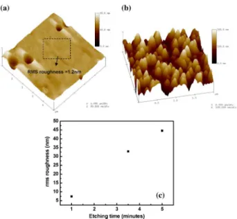
Samples used in this experiment were all grown by metal–organic chemical vapor deposition with a rotating-disk reactor (Emcore D75) on c-face sapphire (0001) substrates. The structure of the LEDs consist a 30-nm-thick low-tempera-ture GaN nucleation layer, a 4- m-thick Si-doped GaN layer, an undoped five-period InGaN-GaN multiple quantum-well (MQW) active region with emission at 470 nm at 20-mA operation, and a 0.1- m-thick Mg-doped GaN. The fab-rication process of the LLO-LEDs on Si began with the deposition of transparent contact ITO, alumina mirror, and indium bonding layer on p-GaN. The sample was then bonded onto an Cr–Au-coated Si substrate at 350 C to form a structure of sapphire–GaN LED/ITO/Al–In–Au–Cr–Si. The bonded structure was subjected to the LLO process to form a u-GaN/n-GaN/MQW/p-GaN structure on Si. A KrF excimer laser (Lambda Physick LPX200) at wavelength of nm with pulsewidth of 25 ns was used to remove the sapphire substrate. The incident laser flux was set to a value of about 0.6 J/cm . The laser beam with a size of 1.2 mm 1.2 mm was incident from the polished backside of the sapphire substrate into the sapphire–GaN interface to decompose the GaN into Ga and N . After the whole GaN LED sample was scanned by the laser beam, the sample was placed on a hot plate at Ga melting point of about 30 C to separate the GaN LED structure from sapphire substrate to form an LLO u-GaN/n-GaN/MQW/p-GaN structure on Si substrate. The details of the LLO process can be described in [4]. Then the u-GaN was etched away to expose the n-GaN layer by inductively coupled plasma reactive ion etching (ICP-RIE) (SAMCO ICP RIE 101ipH). Fig. 1(a) shows the atomic force microscopy (AFM) image of the sample sur-face. The etched sample shows a smooth surface with an rms roughness of around 1.2 nm. The etching process to form
850 IEEE PHOTONICS TECHNOLOGY LETTERS, VOL. 19, NO. 11, JUNE 1, 2007
Fig. 1. (a) AFM image of the sample surface before the nano-roughening process, (b) AFM image of roughened surface with an etching time of 3.5 min, and (c) rms value of surface roughness as a function of the etching time.
face roughness was then performed under a zero bias condition in the ICP-RIE chamber (Cl Ar sccm, 6-Pa chamber pressure, 500-W ICP power) with three different etching time (1, 3.5, and 5 min). Then, a square mesa of m was created by ICP/RIE for current isolation purpose. Finally, a Ti–Al with a diameter of 100- m circular pad was deposited as the n-type contact.
Fig. 1(b) and (c) shows the AFM image of roughened face with an etching time of 3.5 min and the rms value of sur-face roughness as a function of the etching time, respectively. The rms value of surface roughness is 7.4, 32.9, and 44.6 nm for these three conditions. Fig. 2(a) shows the scanning emis-sion microscopy (SEM) images of our fabricated device and the surface roughness. The surface roughness was made at the light-emitting region. Obviously, the “cone” shape roughness densely covered on the surface of LLO LED. From both SEM and AFM images, the height of the GaN cone was revealed to be around 50, 150, and 500 nm at the etching time of 1, 3.5, and 5 min, respectively. The transmission electron microscopy image of the GaN cone was also measured as shown in Fig. 2(b). The dislocation could be found around the bottom of the GaN cone. Besides, the angle between the side plane and basal plane of the cone is around 58 , which suggests the side plane might be plane [13]. These seem to mean the formation of this kind of roughness results from two possible reasons: one is the higher etching rate at the dislocation region than other regions and another is the etching-resistant property of plane [13].
Current–voltage ( – ) characteristics and intensity–current ( – ) characteristics of the nanoroughened LEDs with etching time of 1 min (LED I), 3.5 min (LED II), 5 min (LED III), and conventional LED were measured as shown in Fig. 3(a). It was found that the – curves were almost identical for these de-vices. The 20-mA forward voltages were all around 4.5 V for these three LEDs. The slightly high forward voltage might re-sult from the existence of the residual undoped GaN caused by slightly inaccurate etching rate in the process of removing un-doped GaN. The similarity of electrical property indicates that
Fig. 2. (a) SEM images of our fabricated device and the surface roughness, and (b) transmission electron microscopy (TEM) image of the GaN cone spreading on sample surface.
Fig. 3. (a)I–V and L–I characteristics of the LED I, LED II, LED III, and conventional LED. (b) Wall-plug efficiency and enhancement on light–output power as a function of the rms roughness of top surface we etched.
the fabrication of roughness would not result in any degrada-tion in the electrical properties of nitride-based LEDs. In the light–output power measurement, the device was put in an in-tegral sphere and detected by a calibrated large area Si photo-diode at room temperature. This detecting condition covers al-most all the power emitting from LEDs. It could be seen that EL intensity of LEDs I, II, and III were all larger than that ob-served from the conventional LED. At an injection current of 20 mA, it could be found that the light–output power of LED I, LED II, LED III, and conventional LED was about 9.98, 14.96, 16.29, and 7.67 mW, respectively. The two possible reasons
KAO et al.: LIGHT–OUTPUT ENHANCEMENT OF NANO-ROUGHENED GaN LLO LEDs FORMED BY ICP 851
Fig. 4. Intensity distribution of (a) LED II and (b) conventional LED with a 20-mA injection current.
for the light–ouput enhancement are the reduction of absorp-tion length in vertical direcabsorp-tion and the light scattering from the roughened surface. In our experiment, the thickness of full struc-ture would be varied from 3.5 to 3 m as the etching time was increased to 5 min. We evaluated the effect of the thickness on the light–output intensity using the ray tracing method. In fact, the effect seems to be small and can be neglected in our experi-ment. This also suggests the enhancement of light–output power could be mainly attributed to the much more light scattering from the nano-roughened surface. Fig. 3(b) shows the enhance-ment on light–output power, wall-plug efficiency as a function of the rms roughness of top surface we etched. The enhancement could be significantly raised from 33% to 110%, and wall-plug efficiency could be increased from 7.65% to 17.88% as the rms roughness was increased from 7.4 nm etching time min to 44.6 nm etching time min . However, the enhancement and wall-plug efficiency has shown a tendency toward satura-tion as the etching time was beyond 3.5 min although the rms roughness (44.6 nm) and cone height (500 nm) caused by 5-min etching is greatly larger than those caused by 3.5-min etching.
To further investigate the influence of nano-roughened sur-face on light–output performance of an LED chip, intensity dis-tribution measurements were performed on LED II and con-ventional LED. Fig. 4(a) and (b) shows the photos of LED II and conventional LED with injecting a 20-mA dc current in these two different devices, respectively. Each intensity distri-bution was also shown in the same figure. The EL intensities observed from LED II were obviously greater than those ob-served from conventional LED at the same injection current at the top surface area. Such an enhancement could be attributed to the nano-roughened surface that photons could have a larger probability to be emitted from the device in the top emission di-rection and, thus, achieve even brighter LEDs.
In summary, we have investigated the fabrication and charac-teristics of nano-roughened LLO LED with different rms sur-face roughness using a controllable ICP-RIE dry etching
tech-nique. Using this fabrication method to form nano-scaled rough-ness, the electrical property was almost not degraded below the etching time of 5 min. The light–output power of LLO LED could be significantly enhanced from 7.65 mW (conventional LED) to 16.29 mW (LED III), indicating a higher light extrac-tion efficiency in the structure of nano-roughened LLO-LED. Furthermore, the wall-plug efficiency was also increased from 8.6% to 17.88%. That is, a great enhancement (about two times) has been achieved on both light–output power and wall-plug ef-ficiency of LLO LED using this simple method.
ACKNOWLEDGMENT
The authors would like to thank Prof. K. M. Lau of Hong Kong University of Science and Technology and Prof. Pilkuhn of the University of Stuttgart, Germany, and National Chiao Tung University for useful discussions.
REFERENCES
[1] M. Koike, N. Shibata, H. Kato, and Y. Takahashi, “Development of high efficiency GaN-based multi-quantum-well LEDs and their appli-cations,” IEEE J. Sel. Topics Quantum Electron., vol. 8, no. 2, pp. 271–277, Mar./Apr. 2002.
[2] W. S. Wong, T. Sands, N. W. Cheung, M. Kneissl, D. P. Bour, P. Mei, L. T. Romano, and N. M. Johnson, “ In Ga N light emitting diodes on Si substrates fabricated by Pd-In metal bonding and laser lift-off,”
Appl. Phys. Lett., vol. 77, pp. 2822–2824, 2000.
[3] B. S. Tan, S. Yuan, and X. J. Kang, “Performance enhancement of InGaN light-emitting diodes by laser lift-off and transfer from sapphire to copper substrate,” Appl. Phys. Lett., vol. 84, pp. 2757–2759, 2004. [4] C. F. Chu, F. I. Lai, J. T. Chu, C. C. Yu, C. F. Lin, H. C. Kuo, and S. C.
Wang, “Study of GaN light emitting diodes fabricated by laser lift-off technique,” J. Appl. Phys., vol. 95, pp. 3916–3922, 2004.
[5] J. T. Chu, H. C. Kuo, C. C. Kao, H. W. Huang, C. F. Chu, C. F. Lin, and S. C. Wang, “Fabrication of p-side down GaN vertical light emitting diodes on copper substrates by laser lift-off,” Phys. Stat. Sol. (c), vol. 1, pp. 2413–2416, 2004.
[6] C. Huh, K. S. Lee, E. J. Kang, and S. J. Park, “Improved light-output and electrical performance of InGaN-based light-emitting diode by microroughening of the p-GaN surface,” J. Appl. Phys., vol. 93, pp. 9383–9385, 2003.
[7] T. Fujii, Y. Gao, R. Sharma, E. L. Hu, S. P. DenBaars, and S. Naka-mura, “Increase in the extraction efficiency of GaN-based light-emit-ting diodes via surface roughening,” Appl. Phys. Lett., vol. 84, pp. 855–857, 2004.
[8] D. W. Kim, H. Y. Lee, M. C. Yoo, and G. Y. Yeom, “Highly effi-cient vertical laser-liftoff GaN-based light-emitting diodes formed by optimization of the cathode structure,” Appl. Phys. Lett., vol. 86, pp. 052108-1–052108-3, 2005.
[9] H. W. Huang, C. C. Kao, J. T. Chu, H. C. Kuo, S. C. Wang, and C. C. Yu, “Improvement of InGaN–GaN light-emitting diode performance with a nano-roughened p-GaN surface,” IEEE Photon. Technol. Lett., vol. 17, no. 5, pp. 983–985, May 2005.
[10] D. Eisert and V. Harle, “Simulations in the development process of GaN based LEDs and laser diodes,” in Int. Conf. Numerical Simulation
of Semiconductor Optoelectronic Devices, 2002, Session 3: Photonic
Devices, invited paper.
[11] C. C. Kao, H. C. Kuo, H. W. Huang, J. T. Chu, Y. C. Peng, Y. L. Hsieh, C. Y. Luo, S. C. Wang, C. C. Yu, and C. F. Lin, “Light-output enhancement in a nitride-based light-emitting diode with 22 undercut sidewalls,” IEEE Photon. Technol. Lett., vol. 17, no. 1, pp. 19–21, Jan. 2005.
[12] J. K. Kim, H. Luo, Y. Xi, J. M. Shah, T. Gessmann, and E. F. Schubert, “Light extraction in GaInN light-emitting diodes using diffuse omni-directional reflectors,” J. Electrochem. Soc., vol. 153, pp. G105–G107, 2006.
[13] T. Palacios, F. Calle, M. Varela, C. Ballesteros, E. Monroy, F. B. Naranjo, M. A. Sánchez-García, E. Calleja, and E. Muñoz, “Wet etching of GaN grown by molecular beam epitaxy on Si(111),”