Electrically injected 1.3-
μm quantum-dot
photonic-crystal surface-emitting lasers
M
ING-Y
ANGH
SU,
1G
RAYL
IN,
1,*ANDC
HIEN-H
UNGP
AN21Department of Electronics Engineering and Institute of Electronics, National Chiao Tung University, No. 1001, University Road, Hsinchu City 30010, Taiwan
2Research and Development Division, TrueLight Corporation, Hsinchu City 30010, Taiwan
Abstract: We have fabricated electrically injected InAs/InGaAs/GaAs quantum-dot (QD)
photonic-crystal (PC) surface-emitting lasers (SELs) and successfully demonstrated room-temperature lasing emissions at 1.3-μm wavelength for the first time. The PCSEL device fabrication was greatly simplified by deposition of transparent conducting layer of indium-tin-oxide over “PC slab-on-substrate” structure. The threshold current density per QD layer was as low as 50 A/cm2/layer; however, the optical output was limited to 2 mW. The
band-edge lasing mode was identified and near-circular beam with narrow divergence angle less than 2° was achieved.
© 2017 Optical Society of America under the terms of the OSA Open Access Publishing Agreement
OCIS codes: (250.5590) Quantum-well, -wire and -dot devices; (350.4238) Nanophotonics and photonic crystals; (140.7270) Vertical emitting lasers; (140.5960) Semiconductor lasers; (140.2020) Diode lasers.
References and links
1. S. Noda, M. Fujita, and T. Asano, “Spontaneous-emission control by photonic crystals and nanocavities,” Nat. Photonics 1(8), 449–458 (2007).
2. K. Hirose, Y. Liang, Y. Kurosaka, A. Watanabe, T. Sugiyama, and S. Noda, “Watt-class power, high-beam-quality photonic-crystal lasers,” Nat. Photonics 8(5), 406–411 (2014).
3. M. Imada, A. Chutinan, S. Noda, and M. Mochizuki, “Multidirectionally distributed feedback photonic crystal lasers,” Phys. Rev. B 65(19), 165306 (2002).
4. C. H. Pan, C. H. Lin, T. Y. Chang, T. C. Lu, and C. P. Lee, “GaSb-based mid infrared photonic crystal surface emitting lasers,” Opt. Express 23(9), 11741–11747 (2015).
5. M. Kim, C. S. Kim, W. W. Bewley, J. R. Lindle, C. L. Canedy, I. Vurgaftman, and J. R. Meyer, “Surface-emitting photonic-crystal distributed-feedback laser for the midinfrared,” Appl. Phys. Lett. 88(19), 191105 (2006).
6. T. C. Lu, S. W. Chen, L. F. Lin, T. T. Kao, C. C. Kao, P. Yu, H. C. Kuo, S. C. Wang, and S. Fan, “GaN-based two-dimensional surface-emitting photonic crystal lasers with AlN/GaN distributed Bragg reflector,” Appl. Phys. Lett. 92(1), 011129 (2008).
7. M. Imada, S. Noda, A. Chutinan, T. Tokuda, M. Murata, and G. Sasaki, “Coherent two-dimensional lasing action in surface-emitting laser with triangular-lattice photonic crystal structure,” Appl. Phys. Lett. 75(3), 316– 318 (1999).
8. T. Sakaguchi, W. Kunishi, S. Arimura, K. Nagase, E. Miyai, D. Ohnishi, E. Miyai, K. Sakai, and S. Noda, “Surface-Emitting Photonic-Crystal Laser with 35W Peak Power,” in Technical Digest of Conference on Lasers
and Electro-Optics (CLEO, 2009), paper CTuH1.
9. H. Matsubara, S. Yoshimoto, H. Saito, Y. Jianglin, Y. Tanaka, and S. Noda, “GaN photonic-crystal surface-emitting laser at blue-violet wavelengths,” Science 319(5862), 445–447 (2008).
10. M. Nomura, S. Iwamoto, A. Tandaechanurat, Y. Ota, N. Kumagai, and Y. Arakawa, “Photonic band-edge micro lasers with quantum dot gain,” Opt. Express 17(2), 640–648 (2009).
11. F. Bordas, C. Seassal, E. Dupuy, P. Regreny, M. Gendry, P. Viktorovitch, M. J. Steel, and A. Rahmani, “Room temperature low-threshold InAs/InP quantum dot single mode photonic crystal microlasers at 1.5 µm using cavity-confined slow light,” Opt. Express 17(7), 5439–5445 (2009).
12. T. S. Chen, Z. L. Li, M. Y. Hsu, G. Lin, and S. D. Lin, “Photonic crystal surface emitting lasers with quantum dot active region,” J. Lightwave Technol. 35(20), 4547–4552 (2017).
13. T. Y. Chang, C. H. Pan, K. B. Hong, C. H. Lin, G. Lin, C. P. Lee, and T. C. Lu, “Quantum-dot surface emitting distributed feedback lasers using indium–tin–oxide as top claddings,” IEEE Photonics Technol. Lett. 28(15), 1633–1636 (2016).
14. X. Huang, A. Stintz, C. P. Hains, G. T. Liu, J. Cheng, and K. J. Malloy, “Efficient high-temperature CW lasing operation of oxide-confined long-wavelength InAs quantum dot lasers,” Electron. Lett. 36(1), 41–42 (2000). 15. Y. Liang, T. Okino, K. Kitamura, C. Peng, K. Ishizaki, and S. Noda, “Mode stability in photonic-crystal
surface-emitting lasers with large κ1DL,” Appl. Phys. Lett. 104(2), 021102 (2014).
#307491 https://doi.org/10.1364/OE.25.032697
16. Y. Kurosaka, K. Sakai, E. Miyai, and S. Noda, “Controlling vertical optical confinement in two-dimensional surface-emitting photonic-crystal lasers by shape of air holes,” Opt. Express 16(22), 18485–18494 (2008). 17. Y. Liang, C. Peng, K. Sakai, S. Iwahashi, and S. Noda, “Three-dimensional coupled-wave analysis for
square-lattice photonic crystal surface emitting lasers with transverse-electric polarization: finite-size effects,” Opt. Express 20(14), 15945–15961 (2012).
18. K. Sakai, E. Miyai, and S. Noda, “Coupled-Wave Theory for Square-Lattice Photonic Crystal Lasers With TE Polarization,” IEEE J. Quantum Electron. 46(5), 788–795 (2010).
19. E. Miyai, K. Sakai, T. Okano, W. Kunishi, D. Ohnishi, and S. Noda, “Lasers producing tailored beams,” Nature 441(7096), 946 (2006).
20. A. L. Korotkov, A. G. U. Perera, W. Z. Shen, J. Herfort, K. H. Ploog, W. J. Schaff, and H. C. Liu, “Free-carrier absorption in Be- and C-doped GaAs epilayers and far infrared detector applications,” J. Appl. Phys. 89(19), 3295–3300 (2001).
1. Introduction
Two-dimensional (2D) Photonic-crystal (PC) structures are widely applied in active and passive optoelectronic devices to modify spatial or spectral mode of optical light [1,2]. Surface-emitting lasers (SELs) incorporating 2D-PC emerge as promising photonic devices due to their advantages of nearly symmetric beam and narrow divergence angle for fiber coupling as well as IC-like array manufacturability and testing. One type of them is photonic defect lasers where artificial defects are engineered in 2D-PC to create localized modes in photonic bandgap. Nevertheless, they are subjected to low surface-emitted power in sub-microWatt order because of high quality factor formed in micro- or nano-cavities [1]. Another type is Photonic band-edge lasers, also known as photonic-crystal surface-emitting lasers (PCSELs), where 2D cavity mode is constructed over a large area of 2D-PC without microdefect [2,3]. Coherent light emissions from optical gain media, designed around the edge of photonic band structure, propagate with zero group velocity and strongly couple with 2D-PC structure where in-plane multidirectional distributed feedback (DFB) diffract vertically [3]. The output beam emitted in the direction normal to the 2D-PC plane has narrow beam divergence due to coherent oscillation in large area. Moreover, single longitudinal and transverse mode oscillation has been achieved with a large lasing area, enabling high-power and single-mode operation [2,3].
It is by no means easy to electrically drive PCSELs because injected current flows through unetched part of 2D-PC and is on the same path as emitted light. Therefore, optically pumped PCSELs were realized in demanding materials such as GaSb-based materials [4,5] and GaN-based materials [6]. The first electrically injected PCSEL was demonstrated in 1999 by wafer fusion bonding technique [7]. InP-based slab waveguide with InGaAsP multiple-quantum-well (MQW) active region was bonded over PC-patterned wafer, and then substrate with slab waveguide was selectively etched off. The threshold current density was estimated to be 3.2 kA/cm2 under room-temperature (RT), pulsed operation. Later in 2009, GaAs-based slab
waveguide with InGaAs MQW was bonded over PC-patterned wafer with bottom distributed Bragg reflector (DBR). Extremely high output power of 35 W with slope efficiency of 0.7 W/A was achieved under RT, pulsed operation [8]. As an alternative to wafer fusion, epitaxial regrowth over PC was developed and PCSELs were electrically injected with exciting success. In 2008, GaN-based PCSEL with InGaN MQW was operated under RT, pulsed condition. The threshold current and equivalent current density was as high as 6.7 A and 67 kA/cm2, respectively [9]. Later in 2014, GaAs-based PCSEL with InGaAs MQW was
operated under RT, continuous-wave (CW) condition and light output was as high as 1.5 W [2].
Quantum dot (QD) gain media are versatile for applications in tunable and mode-locked light sources. GaAs-based In(Ga)As QD lasers, in particular, are novel and low-cost solution for long-wavelength gap between 1100 nm and 1300 nm. PCSELs with QD gain were reported only to be optically pumped; electrical injection may not be practical because of “suspended PC slab” design used therein [10,11]. We demonstrated the first RT and optically pumped InAs QD PCSELs of 1.3-μm wavelength range using “PC slab-on-substrate” design
in the previous work [12]. Also in our previous work, electrically injected QD SELs were made possible by depositing indium-tin-oxide (ITO) over one-dimensional (1D) DFB grating or 1D-PC [13]. In this present work, we have fabricated electrically injected InAs QD PCSELs using the same “PC slab-on-substrate” design and successfully demonstrated RT lasing emissions at 1.3-μm wavelength. No complicated techniques of epitaxial regrowth or wafer fusion bonding were involved in the device fabrication. Instead, the epitaxial structure was properly doped and ITO was used for electrical current spreading as well as optical light transmission.
2. Experimental details
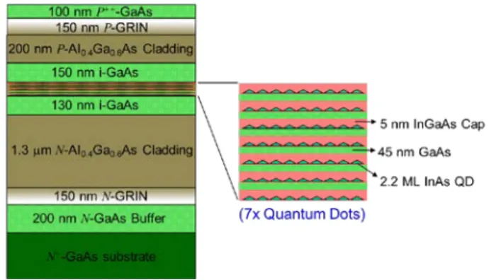
The wafer sample under investigation was grown on n-type GaAs (001) substrate by molecular beam epitaxy. Figure 1 shows the schematic layer structure along with QD active region. If not specified otherwise, silicon and beryllium were doped to 1018 cm−3 for n-type
and p-type doping, respectively. The growth started with 200-nm n-doped GaAs buffer layer, 130-nm n-doped graded-index (GRIN) layer of AlGaAs, 1300-nm n-doped bottom cladding layer of Al0.4Ga0.6As, followed by 150-nm undoped GaAs
separate-confinement-heterostructure (SCH) layer, and proceeded to undoped active region. It consisted of seven layers of 2.2-monolayer InAs QDs, which was capped by 5-nm In0.15Ga0.85As and spaced by
45-nm GaAs. Afterwards, another 150-nm undoped GaAs SCH layer was grown, followed by
p-doped 200-nm top cladding layer of Al0.4Ga0.6As, 150-nm p-doped GRIN layer of AlGaAs,
and ended with 100-nm, p+-doped (~1019 cm−3) GaAs as contact layer. The InAs QD areal
density per layer was close to 3 × 1010 cm−2. It is worth mentioning that the grown structure
incorporated thin upper cladding design so that 2D-PC fabricated afterward was sufficiently close to active region and adjacent diffraction coupling was effectively achieved.
Fig. 1. The schematic layer structure, along with QD active region, of investigated sample.
The PCSELs were designed for the transverse electric (TE) mode in 2D square lattice operated at Γ band-edge. Figure 2(a) shows schematic cross-section of electrically injected QD PCSEL. The fabrication started with 150-nm Si3N4, which was deposited at 300 °C by
plasma enhanced chemical vapor deposition (PECVD) as a hard mask. The PC pattern with circular shaped air holes was defined by e-beam lithography within area of 300 × 300 μm2
and dry etched by inductively coupled plasma. After removing hard mask, mesa of 310 × 310 μm2 was wet etched and another 120-nm Si
3N4 passivation layer was deposited at 80 °C.
Then, circular dielectric aperture of 150-μm diameter was opened by lift-off process. Next, transparent conducting layer of 225-nm indium-tin-oxide (ITO) was deposited by E-gun evaporator at 300 °C. Then, p-type metallization of Ti/Au was deposited for subsequent photoresist lift-off. Finally, n-type metalization of Ni/Ge/Au was deposited and annealed at 420 °C. Figure 2(b) shows the tilted-angle cross-sectional image from scanning electron microscope (SEM). The ITO completely covered the PC structure with small pits over air
holes. The top-view image from stereo optical microscope (SOM) is shown in Fig. 2(c). The outer and inner side-length of square metal aperture is 650 μm and 300 μm, respectively.
Fig. 2. Electrically injected PCSEL with its (a) schematic section, (b) tilted-angle cross-sectional image from SEM, and (c) top-view image from SOM
The grown sample was characterized by photoluminescence (PL) with excitation source of 1064-nm pulsed fiber laser (50 ns pulse width @ 5 KHz repetition rate). The ground-state (GS) energy of InAs QDs was around 1297 nm, and first excited-state (ES) energy was around 1205 nm. Three lattice periods of 388, 390, and 393 nm are patterned so that the design wavelength was around the gain peak of GS-QD. The air-hole filling factor, which is defined as area of unit lattice occupied by air holes, was designed to be 0.1. Based on our previous work, the etched PC depth of QD PCSELs is more than two times that of typical QW PCSELs because QD active region is optically confined tightly and peak modal gain is relatively low [12]. The etched PC depth in this work was about 550 nm. The intermediate-stage devices, right after PC etching but before metallization, were optically pumped by 1064-nm pulsed fiber laser as we performed in [12]. If pumping threshold is not low enough, one can repeat dry etching again for enhanced diffraction coupling. Final electrical characterizations were performed under pulsed current with repetition rate of 1 KHz. The duration of current pulse varied with different measurement conditions. All measurements were temperature controlled by thermoelectric cooler. The emission spectra were then collected by monochromator equipped with InGaAs detector. The spectral resolution is as low as 0.05 nm.
3. Results and discussions
The lasing wavelengths for electrically driven QD PCSELs with lattice period of 388, 390, and 393 nm were measured to be about 1291.7, 1297.6, and 1306.7 nm, respectively. The lowest threshold current was achieved for 390-nm-period PCSEL device. It was consistent with optically pumped results that lower threshold device corresponded to smaller wavelength detuning between PC resonant wavelength and GS-QD gain peak [12]. Figure 3 shows the pulsed L-I-V characteristics and lasing spectra of 390-nm-period QD PCSEL at RT of 20 °C. The 1-KHz current pulse with pulse duration of 1 μs and 5 μs were set in Figs. 3(a) and 3(b), respectively. The series resistance extracted at 100 mA was about 8~9 ohm. The joule heating, constituted 30~50% of the input power, was rather serious. It limited our PCSEL devices tp pulsed operation, and the light intensity exhibited roll over around 300 mA. Moreover, the electrical injection was spatially non-uniform and crowded around the edge of dielectric aperture as revealed in the NFP image at the end of this section. Our separate experiment shown higher annealing temperature above 450 °C was necessary to form good ohmic contact between ITO and p+-GaAs. Further improvement can be expected by
Fig. 3. (a) L-I-V characteristics and (b) lasing spectra of 390-nm period QD PCSEL.
The optical power in Fig. 3(a), measured by a calibrated Ge detector, was limited to 2 mW at injection current of 300 mA. The threshold current was 62 mA and its equivalent threshold current density, spread over circular aperture of 150-μm diameter, was about 350 A/cm2. The
threshold current density per QD layer was as low as 50 A/cm2/layer, which was compared
with the state-of-the-art QD edge emitter of 12 A/cm2/layer [14]. In spectra measurement, the
lasing linewidth in Fig. 3(b) evolved from 0.24 nm at slight above threshold to 0.36 nm at about two times the threshold. The increased linewidth was also observed in [15], where competing side-modes were excited at the longer wavelength side of the main lasing mode at higher current level. These side-modes are group of multiple resonant states which exist for each band-edge mode [15]. They originate with quantized wavevector within finite-size laser cavity and associated with fabrication imperfection and disorder [15]. Moreover, the quality (Q) factor at injection current of 65 mA was a little more than 5000. The high Q factor was associated with low threshold current of 50 A/cm2/layer and low output power.
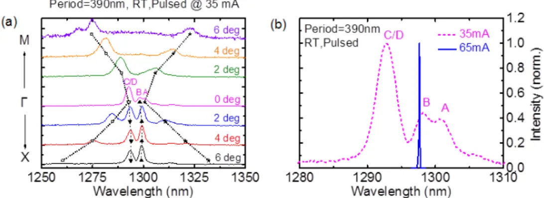
The photonic band structure of square-lattice PCSELs can be constructed from measurement of angle-dependent spectra well below lasing threshold along different in-plane directions. Figure 4(a) shows the below-threshold spectra of our square-lattice, 390-nm-period PCSEL along Γ-X and Γ-M directions with angular step of 2°. They were taken at injection current of 35 mA. The spectra were normalized and shifted in vertical axis so that, when rotated 90° clockwise, they were in the same sense as the typical band structure calculated in [16,17]. The duration of current pulse was increased to 50 μs for enhanced signal detection. Four band-edge modes in the vicinity of Γ point were designated as modes A, B, C and D in order of decreasing wavelength. Note that modes C and D were degenerate modes.
Fig. 4. (a) Angle-dependent spectra along Γ-X and Γ-M with angular step of 2°. (b) Emission spectra below and above threshold current.
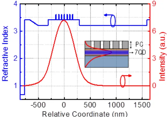
Figure 4(b) shows the emission spectra below and above threshold. The normalized frequencies of band-edge modes A, B, and C/D, in unit of lattice period over wavelength, were 0.29986, 0.30042, and 0.30167, respectively. The normalized frequency difference between modes A and B was ~5.6 × 10⁻⁴, which is about one-quarter to one-third of reported value in [2]. The small mode frequency difference indicates weak 2D feedback coupling because of low confinement factor within the PC layer [2], while QD active region is optically confined tightly [12]. Figure 5 shows the refractive index profile of investigated structure with corresponding electrical field intensity distribution along crystal growth direction. The 1D intensity overlap in QD gain media and PC region is about 15.7% and 14.8%, respectively. If QD area coverage of 0.1 is considered, the confinement factor of QD gain media is only 1.6%.
Fig. 5. The refractive index profile of investigated structure with corresponding electrical field intensity distribution along crystal growth direction.
In Fig. 4(b), the QD PCSEL was observed to lase at mode B instead of mode A. It was reported in [17] that mode A was favored with threshold-gain discrimination of over 20 cm−1 against mode B for device length of 70 μm, and this discrimination decreased with increasing device length. However, our PCSEL was with larger device length of 150 μm. Moreover, with weaker 2D coupling revealed above, we can expect even lower mode selectivity between modes A and B [18]. Since Mode-B wavelength was 2.4 nm shorter than mode-A wavelength, and both were in the long-wavelength side of GS-QD gain peak. The smaller wavelength detuning of mode B was mostly credited for the observed lasing emissions.
Figure 6 shows the near-field pattern (NFP), far-field pattern (FFP), and polarization pattern (PP) of QD PCSEL with lattice period of 390 nm. The NFP images shown in Fig. 6(a) were taken by charge-coupled-device (CCD) camera. It was clearly shown that the active PC area, where current was injected, was a circle with 150-μm diameter. The injected current indeed spread over ITO layer and then was forced to enter dielectric aperture. However, stronger light intensity around the aperture edge was observed because of current crowding effect. The FFP images shown in Fig. 6(b) were captured by Hamamatsu optics system of A3267-12 equipped with near infrared camera C5840. The near-circular and single-lobed beam was analyzed to reveal narrow divergence angle of 1.4° at 80 mA, and less than 2° at all current range. In a magnified view, the emitted beam in Fig. 6(b) was donut-like with maximum intensity not at the center, but in a ring-like region. Destructive interference at the center of far-field was observed due to anti-symmetric electric field of lasing mode B or rotational symmetry of circular lattice points [16]. The destructive interference also decreased the output efficiency and limited the output power.
Figure 6(c) shows the PP in half polar plot at injection current of 100 mA. The light intensity was taken by rotating the linear film polarizer before detector and then normalized. The lasing mode B did not have definite polarization. Since the in-plane electric field
distribution is anti-symmetric with respect to the center of circular air hole, the calculated FFP exhibit azimuthal polarization [16–19] and no noticeable intensity variation can be observed by merely rotating the linear polarizer. For applications where specific polarization is required, one can change the shape of PC holes. For example, asymmetric shape of equilateral triangular holes was adopted in [17], and almost linear polarization was demonstrated.
Fig. 6. (a) NFP, (b) FFP and (c) PP of QD PCSEL with lattice period of 390 nm.
In additional to detrimental effect from joule heating and destructive interference, the low slope efficiency in Fig. 3(a) was further addressed. Since the optical power fraction within GaAs contact layer was low (from Fig. 5) and the free-carrier absorption coefficient of p+
-GaAs was less than 100 cm−1 [20], its free-carrier loss was small. The effect of scattering loss was also believed to be insignificant as the threshold current density of PCSEL was rather low. However, ITO acts as metal-like mirror in the infrared range. We prepared separate ITO sample for optical characterization by M-2000 Ellipsometer (J. A. Woollam Co.), the complex refractive index around 1300 nm is 0.68 + i0.22. Considering 3-layer structure of semiconductor/ITO/air, the calculated power reflectance, absorptance, and transmittance at normal incidence is about 40%, 17.5%, and 42.5%, respectively. Less than a half of optical power was extracted as light output. The transmissivity can be increased to 66% if the ITO quality is enhanced to have complex index of 1.0 + i0.1 and its thickness is reduced down to 100 nm. Further improvement is required to optimize the deposition conditions and thickness of ITO.
4. Summary
In this paper, surface lasing emissions are achieved by utilizing band-edge modes of PC in QD gain media. To electrically drive devices, simple deposition of indium-tin-oxide over “PC slab-on-substrate” structure was used instead of complicated fabrication techniques such as sacrificial etching, epitaxial regrowth or wafer fusion bonding. For the first time, QD PCSELs of 1.3-μm wavelength were demonstrated under pulsed current injection at RT.
We have studied laser characteristics of QD PCSEL with 390-nm lattice period as it has minimum wavelength detuning between peak lasing wavelength and GS-QD gain peak. The threshold current density per QD layer was as low as 50 A/cm2/layer, which was credited to
high quality factor. The photonic band structure of PCSEL device was constructed by angle-dependence emission spectra below threshold and band-edge lasing mode above threshold was identified as mode B in common designation. The NFP revealed current crowding around aperture edge; however, single-lobed and donut-like beam with narrow divergence angle less than 2° was obtained from FFP. Moreover, the lasing mode B has no definite polarization
from polarization measurement. The low intensity output limited to 2 mW was discussed in terms of electrical pumping scheme as well as optical lasing mode property.
The 1.3-μm QD PCSELs in this work are promising light sources in metro/access optical fiber communication network. Besides, array manufacturability of PCSELs is also beneficial to application of wavelength-division multiplexing (WDM). In future work, we attempt to reduce the series resistance by improving the contact between ITO and semiconductor, and to increase the light output by engineering the shape of PC holes.
Funding
Ministry of Science and Technology (MOST), Taiwan (MOST 105-2221-E-009-145 and MOST 106-2221-E-009-153); Aiming for the Top University Program, Ministry of Education, Taiwan.
Acknowledgments
The deposition of ITO was credited to Electronic and Optoelectronic System Research Laboratories, Industrial Technology Research Institute (ITRI). The authors would like to appreciate the services and facilities provided by the Center for Nano Science and Technology (CNST) of National Chiao Tung University (NCTU) in Taiwan.