Smart Dielectrics of Fluorinated Silicon Glass Prepared by Liquid
Phase Deposition Method
Ching-Fa Yeh, Tien-Fu Chen, Yueh-Chuan Lee, Chien-Hung Liu, Shyue-Shyh Lin
Institute of Electronics, National Chiao Tung University, Hsinchu, Taiwan, R.O.C
Email:
[email protected] ;Tel:886-3-5712121
ext.54151 ;Fax:886-3-5724241
ABSTRACT
Fluorinated silicon glass (FSG) film prepared by using liquid-phase deposition (LPD) is very potential for use as a smart dielectric owing to its high fluorine concentration (8.6 at %),lowdielectric constant (3.46), low stress (43 Mpa),
low leakage current density (4.6E-9 A/cm2 at 2 MV/cm) and low deposition temperature (room temperature). By temperature difference and conventional water-adding methods, the LPD technologies and the key process parameters affecting the physicochemical properties and the electrical characteristics will be introduced. Furthermore, the LPD FSG has been applied as gate oxide to MOSFET's and polysilicon iTT's. Owing to its novel property of selective deposition, LPD FSG has been also employed to cap the sidewalls for degradation-free damascene trenches, and to fabricate micro contact holes for the nt/p diodes and the Schottky diodes.
Keywords: LPD FSG .
selective.
dielectric
damascene .
RIE
1. INTRODUCTION
The formation of silicon dioxide (Si02) with low-temperature process (LW) has already played an important role in microelectronic technologies, while high-temperature process can redistribute impurities and generate defects. Conventionally, CVD methods are the most typical to form LTP Si02. However, the high quality CVD SiO2 usually requires complex process control and expensive equipment. In recent years, much attention has been paid to the liquid-phase deposited (LPD) oxide technology'3 for its room temperature process and much simple process control. Since fluorine atoms are naturally incorporated into the film during deposition, the fluorinated silicon glass is named LPD FSG (SiO2F).
Liquid-phase deposition (LPD) can be a very novel process for future microelectronicllvlEMS fabrication because (i) it is a room-temperature process, (ii) it never has plasma damage on material surface or the underlying devices, and (iii) FSG can be selectively deposited on silicon or silicon oxide instead of on photoresist, SiN or metal410. In this paper, we will introduce the essential process technology, physicochemical and electrical properties of LPD FSG. And then we will also introduce the applications of LPD FSG as gate insulator to LTP poly-Si lIFT's and MOSFET's. In addition, we will introduce selective liquid-phase deposition (S-LPD) technology, and its applications to degradation-free damascene trenches for low-K Methylsilsesquioxane (MSQ), and to the formation of damage degradation-free micro contact hole.
2. PROCESS
OF LPD FSGToform FSG by using LPD method, the supersaturated silicic acid solution has to be prepared. As shown in
Fig. 1, two methods can be adopted to prepare the supersaturated silicic acid solution. The first one is conventional LPD (C-LPD). 70g of high purity (99.99%) silica powder (SiO2) is added into 1,500ml 4moIIl H2SiF6 solution. After being stirred at 25°C for 17 hrs, the solution can become saturated with silicic acid [Si(OH)4]. After removing the undissolved silica with filter and adding deionized water (H20), the originally saturated solution will become supersaturated. The second one is temperature-difference LPD (TD-LPD). Saturated silicic acid (Si(OH)4) is mainly prepared at 0°C, and then heated to 25 °C for I hr to become supersaturated.
3. PROPERTIES OF LPD FSG
3.1. PHYSICOCHEMICAL PROPERTIES:
Figure 2 shows a typical FTIR spectrum for LPD SiO7F and thermal oxide, respectively. The absorption bands around 1090 cm' and 810 cm' are due to the Si-O-Si vibration. These absorption bands, which are similar to those found in the spectra of thermal oxide, indicate that LPD SiO2F is amorphous in structure. Another main absorption
band around 930 cm1 in the spectra of LPD SiO2F is due to Si-F. As shown in Fig. 3 and Fig. 4, the comparison between TD-LPD and C-LPD FSG in fluorine concentration, dielectric constant, and stress are summarized. Fluorine concentration in TD-LPD film can achieve a value as high as 8.62 atom %, which is obviously higher than 1.8 —6.2 atom % in C-LPD film. This result also indicates that the TD-LPD method is rather effective for increasing the fluorine concentration. The dielectric constant and stress for C-LPD films are within 3.52 — 4.25and within 83 — 104 MPa, respectively. However due to high fluorine concentration, TD-LPD film demonstrates k (3.46) and low-stress (43 MPa) characteristics"'2. Obviously, TD-LPD is superior to C-LPD in preparing low-k and low-low-stress FSG. 3.2. ELECTRICAL PROPERTIES:
As shown in Fig. 5, the J-E characteristics for the TD-LPD FSG films deposited at 15 & 25t are as low as 10 9108 AJcm2. However, for the film deposited at 35t , the current density is over one order of magnitude higher than those deposited at 15 & 25t . Thisis because the film deposited at 35t is porous and contains many defects, forming electrically active traps.
Figure 6 shows the distributions of current density at 2 MV/cm for as-deposited (solid symbols) and annealed films. All the distributions for the deposited films are rather narrow in current density, indicating that the as-deposited films are uniform in electrical property. After annealing at 400t for 30 mm in N2, the median current density (J50) for the film deposited at 15t increases slightly from 6.9x10⁹ to 9.0x10⁹ A/cm2; Jso for the film deposited at 25°C increases by a factor of 5, from 4.6x10⁹ to 2.3x10⁸ A/cm2; for the film deposited at 35t , increases by a factor of 5.6, changing from 3.6x10⁷ to 2x10⁶ A/cm2. Obviously, the annealing can degrade the insulating ability. In particular, the degradation is rather pronounced for the films deposited at 35°C .Sincemore electrically active traps in the bulk can induce a substantially higher leakage current13, the increased J50 can be attributed to the increased trap density. In fact, the Si-O network is not easily decomposed in 400t annealing. In contrast, the weak terminating bonds can be easily removed in annealing with defects generated'4. According to Fig. 5 & 6, the electrical property and the thermal stability are the best for the films deposited below 25°C.
4. LPD FSG AS GATE INSULATOR
4.1. LPD FSG AS GATE INSULATOR FOR LTP POLYSILICON TFT'S
Figure 7 shows a cross-sectional view of the LTP poly-Si TFT. An under-layer of Si02 (5000 A thick) is thermally grown on a (100) silicon substrate. The polysilicon layer (1000 A thick) is prepared by the SPC'516 method. After the polysilicon layer is patterned into islands, as gate insulator, 1000 A-thick LPD oxide is deposited at 25°C with LPD method mentioned above'7. Then gate polysilicon (3500 A thick) was deposited by LPCVD at 620°C and
patterned. P (5 x 1015 cm2, 40 KeY) self-aligned implanted source and drain regions are formed by thermal annealing for 24 hrs at 600°C. After the interlayer of insulator is formed, the contact holes are opened, and an aluminum layer (5000 A thick) is evaporated and patterned. Finally, hydrogenation is performed in a plasma reactor at 300°C for 60 mm. Figure 8 shows the typical transfer characteristics (lD-VG) for W/L = 200tm/10 tm poly-Si TFT's under constant drain voltage of 5 V and 10 V. For these LTP poly-Si TFTs, the excellent characteristic parameters like ON/OFF current ratio of 4.95 x 10⁶ at VD =5V, field effect mobility of 25.5 cm2N•sec at VD =0.1V, threshold voltage of 6.9 V and subthreshold swing of 1.28 V/decade are obtained.
4.2. LPD FSG AS GATE INSULATOR OF MOSFET'S
N-channel MOSFETs with aluminum gates are fabricated on 1-5 fl-cm (100) p-type silicon substrates. A typical cross-sectional view of the MOSFET device is shown in the inset of Fig. 9. The channel length (L) and the channel width (Z) is 20 tm and 942 xm, respectively. The devices are fabricated with conventional four-mask processes without channel implantation. 1000 A-thick LPD FSG formed at 15°C is first used as gate insulator. Because the fluorine will disappear at a temperature over 700°C'7, the processing temperature has been carefully controlled to avoid affecting the LPD oxide. So in the MOSFET processes, thermal diffusion of phosphorus for the source and drain regions is performed before LPD. In addition, we adopt an aluminum gate to replace the
polycrystalline silicon gate, because aluminum evaporation has hardly any thermal effect on LPD oxide. Post-metal annealing at 400°C is the only high temperature process used after LPD oxide. Through the evaluation on electrical
characteristics, the device parameters including threshold voltage (VT), subthreshold swing (S) and mobility (m) are all analyzed.
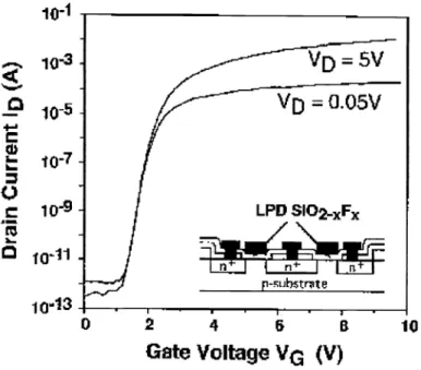
Figure 10 shows the typical ID-VD characteristics of our MOSFET with VG varied in the range from 2 V to 4 V in 0.5 V steps. The triode characteristics and current saturation phenomena well reveals a typical drain
characteristics for a long-channel MOSFET. With accurate plotting of transconductance (pm) versus VG, the 2.1 V of VT 5 obtained. The value of VT is lower than 4 V for the device with different LTP oxide8 indicates that a few oxide charges are contained in the LPD oxide. As shown in Fig. 9, the typical ID-VG characteristics at VD = 0.05 V and 5V, indicates the drain current varies exponentially with VG in the subthreshold region. The peak
transconductance at VD = 0.05 V is 3.68 x iO S. Moreover, the subthreshold slope is 134 mV/decade, which reveals superior to 170 mV/decade of others18. The peak Jteff 5 525 cm2/Vsec, while the peak is 580 cm2! V•sec. In comparison with other works, our peak jt is larger than 413 cm2fVsec but is less than 700 cm2/V•sec'8 of another works. The result shows that the interface properties of SiILPD FSG are superior to those of SiIPECVD Si02. In total the MOSFET with LPD oxide exhibits comparable performance to other low-temperature processed MOSFET.
5. NOVEL APPLICATIONS OF S-LPD FSG
5.1. SIDEWALL CAPPING FOR DEGRADATION-FREE DAMASCENE TRENCHES
As device geometry is scaled down to deep submicron region, a novel intermetal dielectric (liVID) with a low dielectric constant (k) is required to reduce the parasitic capacitance. MSQ, a spin-on organic dielecthc, is very promising as a novel IMD, due to its low k value (2.8— 1 .9) and superior thermal stability (>5OOC)'922. Therefore, damascene interconnection with MSQ dielectrics and copper (Cu) wires, which has a low resistivity, is very promising to solve the RC delay issue. In damascene process, the MSQ film must be first patterned into trenches. However, MSQ film can be easily degraded after resist asking step2123.
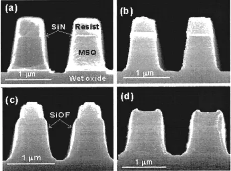
We have proposed sidewall capping technology for degradation-free damascene trenches. Four key process steps, shown in Fig. 1 1, are used to illustrate the preparation of degradation-free MSQ trenches. They are: (a) trench patterning, (b) sidewall cleaning, (c) sidewall capping and (d) resist stripping. A layer of 0.8 tm-thick MSQ was first coated on a 0.6 jtm-thick wet oxide. Next, a layer of 0.04 tm-thick SiN was deposited on the MSQ by plasma-enhanced chemical vapor deposition (PECVD). The MSQ trenches with 0.6 tm linewidth/space were then patterned by using I-line lithography and dry etching (Fig. 1 1(a)). After dry etching, the thin residual polymers left on the sidewalls and the bottoms of MSQ trenches were removed via 02-plasma cleaning,. However, the surface layer on the sidewall of MSQ would also have been slightly oxidized by the treatment, and it should be completely cleared off by wet cleaning in HF-based etching solution (Fig. 1 1(b)). Then a capping layer was selectively deposited on the MSQ sidewalls and the bottoms against the resist by using selective LPD method (Fig.! 1(c)). This selective deposition is based on the mechanism that the LPD film can be only deposited on the surface containing Si-OH bonds24. After sidewall capping, the resist on MSQ was stripped by using conventional ozone ashing (—latm, 300t ,65sec), and cleaned in H2SOIH2O2 solution, and the degradation-free MSQ trenches was finished ( Fig. 1 1 (d)). Figures 12(a)—(d) show the cross-sectional SEM images of degradation-free MSQ trenches corresponding to the four key process steps. It reveals that a thin LPD FSG film has been capped on the sidewalls. Most importantly, S-LPD FSG never caps the resist, therefore there is no problem in stripping resist. MSQ trenches with LPD FSG films on the sidewalls and nitride films on the tops were never exposed and degraded in an oxidizing ambient.
5.2. DAMAGE-FREE CONTACT HOLE FORMATION:
Reactive ion etching (RIE) is widely used to etch silicon oxide to form contact holes because of its anisotropic etching ability. However, RIE process will make surface be damaged and contaminated, resulting in the generation of interface trap at Si02/Si interface and in oxide2526. In addition, the selectivity issue of RIE will become more critical in ultra-shallow junction, because the overetch is less allowed. We have successfully employed a novel selective LPD method to prepare contact holes for the n/p diodes and the Schottky diodes.
As shown in the left side of Fig.13, for the S-LPD samples, the photoresist on the site of contact hole region are first patterned, then the LPD oxide is selectively deposited on the region without photoresist. After oxide deposition and removing photoresist, the contact holes are automatically formed. For the RIE samples, as shown in the right side of Fig. 13, LPD oxide is globally deposited all over the wafers, and the contact holes are formed by using RIE technique
through lithography photoresist patterns. To buffer the damage generation due to RIE, a partial RIE method is adopted. This means that the 85%oxideis etched by RIE, and then the rest 15% oxide is etched by wet-etching in BHF solution. After metallization, some n/p junction diodes are sintered at 400t in N2 for 30mm. For Schottky junction diodes, the N-type (100) wafers with 1—5 a-cm resistivity are adopted. Their fabrication procedures are similar to those of ni/p junction diodes except no ion-implantation process. For both nVp and Schottky junction diodes with contact holes
prepared by S-LPD or RIE method, the I-V characteristics are investigated and compared.
Figure 14(a) shows the comparison of typical I-V characteristics before/after sintering between n/p diodes with contact holes fabricated by S-LPD and RIE. Before sintering, for S-LPD sample the reverse current at 5V reverse bias one order smaller than that for RilE sample. The ideality factor r of S-LPD sample in the forward bias -O.4---O.5V approaches to 1. These results implies that very few G-R centers exist in S-LPD sample, but a lot exist in RIE sample. Besides, the S-LPD samples also exhibit larger forward current. This indicates that there is smaller series resistance in the neutral region of S-LPD diodes. It has been reported that on Si surface RIE easily induces defects, which will result in donor-like charge states. These states will play as G-R centers and increase reverse current if they locate near the band-gap center.
To further study performance of the Si near-surface region for ultra-shallow junction, Schottky diodes were first used for this investigation. Figure 14(b) depicts the performance of S-LPD and RIE Schottky diodes before/after sintering. Before sintering (dash curves), RIE sample nearly loses the rectifying characteristics of Schottky diode under reverse bias, while S-LPD sample exhibits satisfactory Schottky characteristics. However, after sintering (solid curves), the S-LPD sample still exhibits about four orders smaller than that of RIE sampe in reverse current. It is believed that the donor-like bonding defects and the polymer residues make the depletion region be thin and cause the potential barrier lowing, and thereby degrade both reverse and forward I-V characteristics. These results indicate that for the RIE Schottky diodes the sintering is essential to release some of the residues and the defects from the Si surface, but unnecessary for the S-LPD sample. Accordingly RIE process indeed becomes more critical, and requires additional post-treatment. S-LPD can avert these problems and is a good candidate as plasma-damage free, energetic-impurity free and polymer-residue free technology.
6. CONCLUSIONS
LPD FSG technology has been investigated, and its novel applications have also been developed. Using the optimized LPD conditions, the FSG film can be innovatively formed with excellent physicochemical and electrical properties. TD-LPD FSG demonstrates high fluorine concentration (8.6 %), low-k (3.46) and low-stress (43 MIPa) and low leakage current density (4.6E-9 A/cm2 at 2 MV/cm) characteristics. In practical, the applications on poly-Si TFT' s and MOSFET's devices have also proved LPD FSG is a good candidate as LTP gate dielectrics. Besides, the S-LPD technique has overcome many undesirable problems such as RIE-induced damage on contact-hole and ashing-induced degradation on MSQ. The S-LPD method indeed has the following superiorities in forming contact-holes or
degradation-free damascene trenches. From the points of (i) plasma free process, (ii) damage free process, and (iii) residue and contamination free process, the S-LPD will also replace conventional RIE. It is believed that the LPD technologies are able to supply smart dielectrics to various applications in microelectronics/MIEMS.
7. ACKNOWLEDGMENTS
This study is supported by the National Science Council (NSC 89-22 1 8-E-009-08 1).
8. REFERENCE
1. H. Nagayama, H. Honda, and H. Kawahara, J. Electrochem. Soc., 135, 2013 (1988).
2. T. Homma, K. Katoh, Y. Yamada, J. Shimizu, and Y. Murao, in Symp. in VLSI Tech., p. 3 (1990). 3. T. Homma, T. Katoh, Y. Yamada, and Y. Murao, J. Electrochem. Soc., 140, 2410 (1993).
4. CF. Yeh, Y.C. Lee, K.H. Wu, Y.C. Su, S.C. Lee, "Comprehensive Investigation on Fluorosilicate Glass Prepared by Temperature-Difference Based Liquid-Phase Deposition", J. Electrochem. Soc., 147(1), p. 330, 2000
5.CF. Yeh, Y.C. Lee, Y.C. Su, K.H. Wu, C.H. Lin, " Novel Sidewall Capping for Degradation-Free Damascene Trenches of Low-Permittivity Methylsilsesquioxane ",Jpn.J. Appl. Phys. Lell., Vol.39, No. 4B, 2000
6. T. Horiuchi, T. Homma, Y. Murao, and K. Okumura, "An Asymmetric Sidewall Process for High Performance LDD MOSFET's", IEEE Trans. Electron Devices, Vol. 41, p. 186, 1994
7. C.F. Yeh, C.H. Liu, and J.L. Su, "Application of Selective Liquid-Phase Deposition to Fabricate Contact Holes without Plasma Damage", J. Electrochem. Soc., vol. 146, p.2294, 1999
8. CF. Yeh, S.S. Lin, T.Z. Yang, CL. Chen, and Y.C. Yang, "Performance and Off-State Current Mechanism of Low-Temperature Processed Polysilicon Thin-Film Transistors with LPD-Si02 Gate Insulator", IEEE Electron Device, ED-41, No. 2, p. 173, 1994
9. T. Homma, T. Katoh, Y. Yamada, and Y. Murao, "A Selective SiO2 Film-Formation Technology Using Liquid Phase Deposition for Fully Planarized Multilevel Interconnections", J. Electrochem. Soc., vol.140, p.2410, 1993
10. C. F. Yeh et al., "Low-Temperature Processed MOSFET's with Liquid Phase Deposition SiO2F as Gate Insulator", IEEE Electron Device Lett., Vol. 16, No. 7, p. 316, (1995).
1 1. C.F. Yeh, 5.5. Lin, and W. Lur, "Characterization of Dielectric Constant for Liquid-Phase Deposited (LPD) SiOF Films", Proc. of 13th VLSI Multilevel Interconnection Conference (VMIC), p.101, 1996.
12. CF. Yeh, 5.5. Lin, and Water Lu, "Stress in Liquid-Phase Deposited Oxide Films", J. Electochem. Soc., vol. 143, p. 2658, 1996
13. T.H. Fan, 5.5. Lin and C.F. Yeh, "Leakage Current Conduction Mechanism of Liquid Phase Deposited (LPD) SiO2 Film", Extended Abstract of the 1995 International Solid State Devices and Materials (SSDM'95), p.596, 1995 14. A. Yokozawa and Y. Miyamoto, "Oxygen Vacancy with Large Lattice Distortion as an Origin of Leakage Currents
in SiO2", Appl. Phys. Lett., vol. 73, p. 1 122, 1998
15. T.Watanable, H.Watakable, K.Asada, T.Sameshima and M.Miyasaka "Characterization of Electrical and Structureal Properties of Solid Phase Crystallized Silicon Films", TFTp1-4, p1 15 AMLCD 2001.
16. Taizoh Sadoh, Isao Tsunoda, Tomohiro Nagata, Atsushi Kenjo, and Masanobu Miyao "Enhancement of Solid-Phase Crystallization of a-Si on Si02 by Si-Si Bond Modulation," TFTp4-2, p167 AMLCD 2001.
17. C.F. Yeh, CL. Chen, W.Lur, and P.W. Yen,"Bond-structure changes of liquid phase deposited oxide (SiO2F) on N2 annealing," Appl.Phys.Lett.,vol. 66p.938, 1995.
18. S.Suyama, A. Okamoto, and T. Serikawa, "Electrical characteristics of MOSFET utilizing oxygen-argon sputter-deposited gate oxide films," IEEE Trans. Electron Device., vol ED-34, p.2124, 1987.
19. M.T. Bohr, "Interconnect Scaling The Real Limiter to High Performance ULSI", in Tech. Dig. 1995 IEEE mt. Electron Devices Meeting, p.241, 1995.
20. J.F. Remenar et al., "Templating Nano Pores into Poly(Methylsilsesquioxane): New Low-Dielectric Coatings Suitable for Microelectrical Application", in Low-Dielectric Constant Materials IV, Mat. Res. Soc. Symp. Proc., 511, C. Chiang, P.S. Ho, TM. Lu, and J.T. Wetzel, Editors, p. 69, 1998.
21. J.J. Yang, SQ. Wang, L. Forester, and M. Ross, "Integration of Spin-on Low-K Dielectric Using E-Beam Curing for ULSI Multilevel Interconnects", Advanced Metallization for ULSI Application in 1997, eds. R. Cheung, J. Klein,
K. Tsubouchi, M. Marakami, and N. Kobayashi, (MRS, 1997) p. 359., 1997
22. S. Ito, Y. Homma, E. Sasaki, S. Uchimura, and H. Morishima, "Application of Surface Reformed Thick Spin-on-Glass to MOS Device Planarization", J. Electrochem. Soc., Vol. 137 ,p.1212, 1990
23. H. Aoki, S. Yamasaki, T. Usami, Y. Tsuchiya, N. Ito, T. Onodera, Y. Hayashi, K. Ueno, H. Gomi, and N. Aoto, "A Degradation-Free CU/HSQ Damascene Technology using Metal Mask Patterning and Post-CMP Cleaning by
Electrolytic Ionized Water", Tech. Dig. 1997 IEEE mt. Electron Devices Meeting, p. 777., 1997
24. T. Homma, T. Katoh, Y. Yamada, and Y. Murao, "A Selective Si02 Film-Formation Technology Using Liquid-Phase Deposition for Fully Planarized Interconnects", J. Electrochem. Soc., Vol. 140, p.2410, 1993
25. O.O.Awadelkarim, P.I.Mikulan, T.Gu, R.A.Ditizio, and S.J.Fonash, "Hydrogen permeation, Si defect generation, and their interaction during CHF3/02 contact etching," IEEE Electron Device Lett., vol. 15, p.85, 1994.
26. O.O.Awadelkanm, T.Gu, R.A.Ditizio, P.I.Mikulan, S.J.Fonash, J.F.Rembetski, and Y.D.Chan, "Electrical characteristics of the Si substrate in magnetically enhanced or conventional reactive-ion-etch-exposed SiO2/p-Si structure," IEEE Electron Device Lett., vol.14, p.167, 1993.
27. Y.Wang, S.W.Graham, L.Chan, and S.T.Loong, "Understanding of via-etch-induced polymer formation and its removal", J. Electrochem. Soc., vol.144, p 1522, 1997.
C- H2SiF6 4M 15ooj
ci
2C fr
17 1+C Silica-sathrated IjSiF
C- Sffica-supersaated
iF)
I sisub$trate1__..1,(eposition
of C-LPD SiOF at
:-
H2iF6 41i
1500 c.c.
C Stirring at
C for 24 hrsj
1
C
Filtering undissolved1 Silica-saturated
H2SiF6 at 0
[Heated to
JrL Silica-supersaturated
H 2SiF6 ):,
I Si
substrate
(Deposition of TD-LPD Film )
Fig. 1 Flow diagram of C—LPD and TD-LPD process
C,
C
E
C
1-Wavenumber (cm1)
J. C
Fig.4 The comparison of dielectric constant and stress between TD-LPD
and C.-LPD
If
Previous
study
(1
000mI H251F6)10
8
6
4
2
a
I If
UI
This studyif
I (I Without250
750
1250
Writer
QuntiIy
ofWter ( ml)
TD-LPD
C-LPD
Fig.3 The comparison offluorine concentration between TD-LPD and
C-LPD
/
4.5
4.0
3.5 3g0This
I PI'EPViOUSstudy
study
(lOOUm] 1 2SiF) A 4OtPC+. C .
J LIJ 85 50 15 .,This
study
1—U
I -+
171
Preyion
shidy
(lOflimI llSF)Ii"
1O5
15
WaterTD-LPD
250 5cW3 ma
woo Quantity ofWatLr( ml)C-LPD
Wlthovt W2tet TDIILPD :--•• : • -30 250 5XI 750 Q]Itily ofWater( ml)C-LPD
E
'1
Fig. 5
J-F
characteristics for films deposited at 15, 25,
and
35
O(
Fig.6 Distributions of current density at 2MV/cm for the ass-deposited
films (solid symbols) and the annealed films (empty symbols), with
deposition temperature as a parameter.
E (MV/cm)
LI
Fig.7 The cross-sectional view of the fabricated poly-Si 'l'FT's
ir4 W/L=2OOtm/1Otm,/
VDS5V /
—--VDS=1OV/
1011, -, I I-20 -15 -1D -5
0 5 10 15 20 25
VGS (V)
Fig.8
Trensfer characteristics of the n-channel poly-Si IFT
with
LPD
+.J a)
U
C)0
C
I-C
LJ1_J I fl-'- I _____ e101
7O5V
/
LPD SIOF
iO'11icr13
0
2
4
6
B10
Gate
Voltage V (V)
Fig.9
Id-Vg characteristics ofMOSFET's using LPD FSG as gate
insulator
1
2
3
Drain Voltage Vp (V)
Fig. 10 The typical ID-VD characteristics of our MOSFETrs with LPD FSG
(Treiwh Paflerningj
Polymer
Resist
Li L
Wet I7dde
[!ew all CIanini
Sidewall Capinng
(d)
'F
F FF'L.
E'L
Fig. 11 Cross-sectional demonstration for MSQ trenches after (a) trench
patterning, (b) sidewall cleaning, (c) sidewall capping, and (d) resist
stripping
[Resizt Sirippin
3Fig. 12 Cross-sectional SEM images for MSQ
trenches
after (a) trench
patterning, (b) sidewall cleaning, (c) sidewall capping, and (d) resist
. Field Oxide
n implant
-LPD samp/e
R!E samp/e
P. ft LPD -oxide
..
1
'
Ii
se/c cti'ie
'
owtb LPD oxide___ : R
I-,-,-
5]sabstrat
I
A I LPD -oxide
I
subtia
Fig.13
Process-FlowDiagram ofn/pjunction diode with contact hole
fabricated by S-LPD (left) or conventional RIE (right).
(•\ PIE (after)