低耗電的位址匯流排編碼方法
64
0
0
全文
(2) 低耗電的位址匯流排編碼方法 Low-Power Address BUS Encoding. 研 究 生:翁綜禧. Student:Tsung-Hsi Weng. 指導教授:鍾崇斌. Advisor:Chung-Ping Chung. 國 立 交 通 大 學 資 訊 工 程 系 碩 士 論 文 A Thesis Submitted to Department of Computer Science and Information Engineering College of Electrical Engineering and Computer Science National Chiao Tung University in partial Fulfillment of the Requirements for the Degree of Master in. Computer Science and Information Engineering June 2005 Hsinchu, Taiwan, Republic of China. 中華民國九十四年六月.
(3) 低耗電的位址匯流排編碼方法. 學生:翁綜禧. 指導教授:鍾崇斌 博士. 國立交通大學資訊工程學系﹙研究所﹚碩士班. 摘. 要. 近年來如何降低電腦系統中的耗電量已經是個非常重要的課題了。一般 而言,系統中耗用在連接處理器與記憶體之間匯流排上的電量高達 50%以 上,這些電能是被傳送資料時各個匯流排線路產生的電位變化所消耗掉 的,因此藉由資料編碼/解碼方法減少匯流排線路產生的電位變化就成了降 低匯流排耗電量最有效的方法。在此,我針對指令位址匯流排、資料位址 匯流排,以及混和指令/資料位址匯流排分別設計了編碼機制,來減少匯流 排上產生的電位變化,以減少其上的電能消耗。對於指令位址匯流排,設 計了 DAT (Discontinuous Address Table)與 T0 搭配,以同時處理連續位址 以及 branch 指令造成的不連續位址;對於資料位址匯流排,設計了一方法, 其中結合 T0 與 BI、動態改變位址跨距(Stride),以及區別讀/寫位址分別編 碼,可因應資料位址中連續位址與不連續位址混雜的特性來做處理;對於 混和指令/資料位址匯流排,利用了指令記憶體位址與資料記憶體位址之間 的關係,設計了 Stride Table 方法,並與 DAT 搭配,作為此環境的編碼設 計。實驗結果顯示,這樣的方法能夠減少指令位址匯流排上 90.5%的電位 變化、資料位址匯流排上 26%的電位變化、以及混和指令/資料位址匯流排 上 77.4%的電位變化。. -i-.
(4) Low-Power Data Address BUS Encoding Method Student: Tsung-Hsi Weng. Advisors: Dr. Chung-Ping Chung. Department of Computer Science and Information Engineering National Chiao Tung University. ABSTRACT. Reducing power consumption of computer systems has gained much research attention recently. In a typical system, the memory bus power constitute will over 50% of all system power; and this power is required due to bus signal transitions (0Æ1 or 1Æ0). Reducing the number of memory bus transitions is hence an effective way to reduce system power. I present encoding schemes to reduce instruction address bus, data address bus, and instruction/data mixed address bus power consumption. For instruction address bus, T0 with DAT (Discontinuous Address Table) is proposed to handle both consecutive addresses and the branch target addresses; for data address bus, combination of T0 and BI method, variable-stride, and SRWEC (Separated Read/Write Encoding Contents) is proposed to handle both the randomness and continuities of data address sequence; as for instruction/data mixed address bus, DAT is used for instruction address sequence and Stride-Table which can take use of the relationship between instruction address and data address is applied for data address sequence. Simulation results show that the overall bus line switching reduction is 90.5% of unencoded instruction address bus, 26% of unencoded data address bus, and 77.4% of unencoded instruction/data mixed address bus. - ii -.
(5) 誌. 謝. 感謝鍾老師與單老師兩年來的指導,實驗室各位學長同學給予的寶貴意 見,以及家中父母親給予我的關懷和支持。有了這麼多人的幫忙和支持, 我才得以順利完成這份論文。 祝所有幫助過我、關懷過我的人, 身體健康、事事順利!. 翁綜禧 2005/08/29. - iii -.
(6) Table of Contents 摘要. i. ABSTRACT. ii. Table of Contents. iii. List of Figures. v. List of Tables. vii. Chapter 1 Introduction. 1. 1.1 Power Consumption of System Bus. 1. 1.2 The Existing Methods. 2. 1.3 Thesis Organization. 2. Chapter 2 Background. 3. 2.1 How CPU request memory data?. 3. 2.2 Bus Architectures. 5. 2.3 Related Bus Encoding. 6. 2.3.1 Bus-Invert (BI). 6. 2.3.2 Zero-Transition (T0). 8. 2.3.3 Combining T0 & BI (T0_BI) 2.4 Summary & Observation. 11 14. Chapter 3 Designs. 16. 3.1 Design Overview. 16. 3.2 Instruction Address Bus Encoding: T0 with Discontinuous Address Table (T0 DAT) 3.3 Data Address Bus Encoding. 17 22. 3.3.1 Combining T0 & BI using single control line (T0_BI_1). 22. 3.3.2 T0_BI_1 with Variable-Stride capability (T0_BI_1/S). 27. - iv -.
(7) 3.3.3 Preserving Read/Write Continuities in a multiplexed data address sequence (T0_BI_1/S/RW) 3.4 Instruction/Data Mixed Address Bus Encoding. 32 35. 3.4.1 Preserving Instruction/Data Continuities in a multiplexed address sequence (I/D Selector). 36. 3.4.2 Applying different stride value on each data access (Stride-Table). 37. 3.5 Summary. 43. Chapter 4 Simulation. 44. 4.1 Simulation Environment. 44. 4.2 Simulation Results. 47. 4.2.1 Results of Instruction Address Bus Encoding. 47. 4.2.2 Results of Data Address Bus Encoding. 48. 4.2.3 Results of Inst/Data mixed Address Bus Encoding. 49. Chapter 5 Conclusions. 51. Chapter 6 References. 52. 問題討論. 53. -v-.
(8) List of Figures Figure 2.2.1: Bus Architectures-4 Buses. 5. Figure 2.2.2: Bus Architectures-2 Buses. 5. Figure 2.2.3: Bus Architectures-1 Bus. 5. Figure 2.3.1: diagram of Bus-Invert. 6. Figure 2.3.2: Example of Bus-Invert Encoding. 7. Figure 2.3.3: diagram of T0. 9. Figure 2.3.4: Example of T0 Encoding. 10. Figure 2.3.5: diagram of T0_BI. 11. Figure 2.3.6: Example of T0_BI Encoding. 13. Figure 3.1: Address Bus Encoding Architecture. 16. Figure 3.2.1: diagram of T0 DAT. 17. Figure 3.2.2: example of T0 DAT Encoding. 20. Figure 3.3.1: diagram of T0_BI_1. 22. Figure 3.3.2: Example of T0_BI_1. 24. Figure 3.3.3 Special Cases of T0_BI_1. 25. Figure 3.3.4: diagram of T0_BI_1/S. 27. Figure 3.3.5: Example of T0_BI1/S, endurance=1. 30. Figure 3.3.6 T0_BI_1/S/RW block diagram. 32. Figure 3.4.1: diagram of general instruction/data mixed address bus. 35. Figure 3.4.2: diagram of my instruction/data mixed address bus encoding. 35. Figure 3.4.3: diagram of I/D selector. 36. Figure 3.4.4: diagram of I/D selector with T0 DAT and Stride-Table. 37. Figure 3.4.5: example of I/D Selector with T0 DAT and Stride-Table, At Start. 39. Figure 3.4.6: example of I/D Selector with T0 DAT and Stride-Table, Iteration 1. 40. - vi -.
(9) Figure 3.4.7: example of I/D Selector with T0 DAT and Stride-Table, Iteration 2. 41. Figure 3.4.8: example of I/D Selector with T0 DAT and Stride-Table, Iteration 3. 42. Figure 3.4.9: diagram of Stride-Table combining with Bus-Invert. 42. Figure 4.1: Simulation flowchart. 46. Figure 4.2.1: effects of DAT size. 47. Figure 4.2.2: Results of T0 DAT. 48. Figure 4.2.3: Results of T0_BI_1/S/RW. 48. Figure 4.2.4: effects of Stride-Table Size. 49. Figure 4.2.5: Results of I/D Selector with T0 DAT and Stride-Table. 50. - vii -.
(10) List of Tables Table 1: Summary of BI, T0, and T0_BI. - viii -. 14.
(11) 1 Introduction The increase in complexity of system-on-chip (SoC) designs has led to the power consumption, hence cooling, and reliability problems. Power consumption is becoming one of the most important design issues especially for embedded systems. On the other hand, we are witnessing a dramatic market size increase for portable electronic devices such as mobile phones and personal digital assistants. While these products are battery-powered, and their functional requirements due to users are even increasing, low power design for these systems hence becomes a very important research topic.. 1.1 Power Consumption of System Bus In a digital computer system, the major power consumption comes from the off-chip processor-memory bus traffic. And it has been estimated that the capacitance driven by the I/O nodes is usually three orders of magnitude [1] that of the one seen by the internal nodes of a microprocessor. As a result, it is imperative to reduce Bus power for the purpose of low-power. How the system bus consume power? The power consumption equation of typical buses is as following: P = ½ .SBT . Cs . Vdd2 ¾ P:. Power Consumption of Bus. ¾ SBT : the # of bus bit transitions ¾ Cs :. self-capacitance. ¾ Vdd :. Bus supply voltage. Here we can find that the power consumptions of bus are dominated on three parameters: SBT, Cs, and Vdd. For achieving low-power in CMOS circuits, Cs or Vdd must be minimized. Decreasing Vdd has a quadratic effect and is a very efficient way of reducing power consumption. However, the decrease of lower Vdd -1-.
(12) is still not enough[1] as required by portable applications. As a result, lowering Vdd must be done together with other methods for decreasing more power consumption. Here, reducing the bit-transitions (0Î1 or 1Î0) on the bus, means SBT value, is a marvelous way of further decreasing power consumption.. 1.2 The Existing Methods In [4] Stan and Burleson proposed the Bus-Invert method to reduce the bit-transition number of randomly distributed bus patterns. In [5] Benini et al. proposed T0 code to reduce the bit-transition number of consecutive bus patterns, which occupy a large portion in instruction address stream. In [6], Benini et al. proposed T0_BI method. This method can handle both randomly distributed and consecutive patterns. This method can be applied on data address bus, but there are still some improvements can be done. I will show these improvements in this paper.. 1.3 Thesis Organization The rest of the thesis is organized as follows: Section 2 describes the background of low-power address bus encoding. Section 3 presents the proposed designs for reducing the bit transitions on kinds of address buses. Section 4 gives the performance results. The last section summarizes the work.. -2-.
(13) 2 Background In this section, the behaviors of how CPU requests memory data are described. After that, the Bus architecture in general systems and what happened while transmitting address/data via these Buses are introduced. And then I will show you the related low-power bus encoding techniques and some potential improvements to these existing designs. Here, my design issues are also unveiled.. 2.1 How CPU request memory data? While CPU executing programs in a general computer system, the processor will unceasingly access the memory for fetching instructions, reading input data, and write the computation results. All these transmissions have to be done by the system Buses. Following shows the needed transmissions between CPU and memory, and the behaviors of them:. 1. Instruction Address Stream The behavior of instruction address sequence is usually consecutive, and the stride of instruction address is equal to the size of instruction words. The instruction address is usually consecutive under general condition. However, when the branch instructions (goto, if, call, return, etc.) are executed, the next instruction address sequence is depend on the branch result. When branch taken, the next instruction address will not be sequential to the address of the branch instruction. Though the branch target addresses are not sequential to addresses of the branch instructions, the target addresses are seldom changed when program executed. As a result, the behavior of instruction addresses is quite regular and predictable.. -3-.
(14) 2. Data Address Stream The behavior of data address sequence may be randomly distributed at sometimes and sequential at the other time, and the stride of data address will vary with time. The data address is usually randomly distributed under general condition. However, when applications access arrays or scalar data in loops, the accessed data addresses may contain some continuity. Besides this, even if the data addresses are sequential in loop, the stride between addresses will differ with the size of accessed objects and the continuity will be contaminated for the intervention of reads and writes.. 3. Instruction Stream Generally, there are almost no continuity in two instructions, and are never changed after compilation. The behavior of instruction sequence is randomly distributed in the run-time. However, most RISC-based ISAs exhibit some regularity and can be partitioned into fixed-location fields. So many optimizations on instructions are done in the compile time.. 4. Data Stream The behavior of data sequence is randomly distributed in all times. Because the input data may vary with time, the value of data is quite irregular and non-predictable. However, there are some characteristics in data value. For example: leading with 0 or 1, repeating, etc.. This thesis will take the characteristics of instruction address stream and data address stream into consideration in later design.. -4-.
(15) 2.2 Bus Architectures The four streams discussed in previous section are all transmitted though system buses. Now the typical bus architectures are introduced following:. 4 Buses Data Memory. Instruction Address. Data Address CPU. Data. Instruction. Instruction Memory. Figure 2.2.1: Bus Architectures-4 Buses In this Bus architecture, each stream is transmitted using its dedicated bus. Streams will never inference other streams. As a result, the characteristic of the four streams will be preserved on the Bus, and it’s easy to make use of while encoding.. 2 Buses Instruction/Data Address CPU. Instruction/Data. Memory. Figure 2.2.2: Bus Architectures-2 Buses In this architecture, instruction address stream is mixed with data address stream, and instruction stream is mixed with data stream. The stream individualisms are broken because of the intervention of each other. Moreover, the offline optimization of instructions might get poor performance here.. 1 Bus CPU. Instruction/Data Address/Data. Memory. Figure 2.2.3: Bus Architectures-1 Bus In this architecture, all the four streams are mixed together. As a result, almost all characteristics of these streams are broken now. In my thesis, I study the address bus encoding. Buses focused here are instruction address bus and data address bus in “4 Buses” architecture, and instruction/data address bus in “2 Buses” architecture. I will design suitable encoding algorithms for each of the three Bus.. -5-.
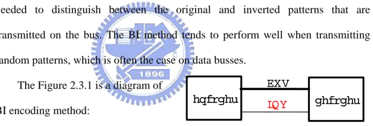
(16) 2.3 Related Bus Encoding Followings are related researches on low-power bus encoding. The Bus-Invert (BI) method is suitable for Common Buses, Zero-Transition (T0) method is design for Instruction Address Bus, and T0_BI design can be applied on Data Address Bus.. 2.3.1 Bus-Invert (BI) In [4] Stan and Burleson proposed the Bus-Invert method as explained next. Consider an N-bit bus. The idea is that if the hamming distance between two consecutive patterns is larger than N/2, then the second pattern can be inverted so as to reduce the inter-pattern Hamming distance to below N/2. One extra bit is needed to distinguish between the original and inverted patterns that are transmitted on the bus. The BI method tends to perform well when transmitting random patterns, which is often the case on data busses.. BUS. The Figure 2.3.1 is a diagram of. encoder BI encoding method:. INV. decoder. Figure 2.3.1: diagram of Bus-Invert Following is the encoding algorithm of this method BI encoding{ int INV; while (receive data address){ current address = received data address; if (transition #>bus_width/2) { INV = 1; data address bus = inverted current address; }else{ INV = 0; data address bus = current address; }}} “INV” means the control signal to be sent to the decoder, “current address” means the address value to be transferred, and the “data address bus” means the code that to be transferred via data address bus.. -6-.
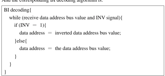
(17) And the corresponding BI decoding algorithm is: BI decoding{ while (receive data address bus value and INV signal){ if (INV = 1){ data address = inverted data address bus value; }else{ data address = the data address bus value; } } } “INV” means the control signal from the encoder, and the “data address” means the real address in this transmittion.. The Figure 2.3.2 shows an example of the Bus-Invert. N o E ncode A d d re ss to b e tra n s fe r. A d d re ss o n B U S. 0000. 0000. 0010. 0010. 7FF0. 7FF0. 7FF2. 7FF2. T o ta l T ra n s itio n s. 12. in itia l. (a): No Encoding. B u s-In v e rt (B I) A d d ress o n B U S. IN V. 0000. 0. 0010. 0010. 0. 7FF0. 800F. 1. 7FF2. 800D. 1. A d d r e s s t o b e tr a n s f e r in it ia l. 0000. T o t a l T r a n s it io n s. 9. (b): Bus-Invert Encoding Figure 2.3.2: Example of Bus-Invert Encoding. 7.
(18) The Figure 2.3.2 shows an easy example of bus transfer. The initial bus value is ‘0000’, the bus width N=16, and the addresses to be transfer with time is ‘0010’ Æ ‘7FF0’ Æ ‘7FF2’. The original non-encoded transfer is shown in Figure 2.3.2a, the total transition number is 12. The BI-encoded transfer is shown in Figure 2.3.2b . While transferring from ‘0000’ to ‘0010’, the Hamming distance is 1, which is less than N/2, so that ‘0010’ is not inverted. While transferring from ‘0010’ to ‘7FF0’, the Hamming distance is 10, larger than N/2, so that ‘7FF0’ is inverted to ‘800F’ and the INV is asserted. Here, the real transition number of this transfer is 6. Next, while transferring from ‘800F’ to ‘7FF2’, the Hamming distance is 15 (note that the real meaning is still from ‘7FF0’ to ‘7FF2’), so it is also inverted to ‘800D’ and the INV is still asserted. The real transition number of this transfer is 1. As a result, the total transition number is 9, and it is better than that of non-encoded bus.. 2.3.2 Zero-Transition (T0) In [5] Benini et al. proposed T0 code technique, which exploits data continuity to reduce the switching activity on the instruction address bus. The observation is that instruction addresses are sequential except when control flow instructions are encountered or exceptions occur. T0 adds a redundant bus line, called INC. If the addresses are sequential, the sender freezes the value on the bus and sets the INC line. Otherwise, INC is de-asserted and the original address is sent. On average 60% reduction in address bus switching activity is achieved by T0 coding.. 8.
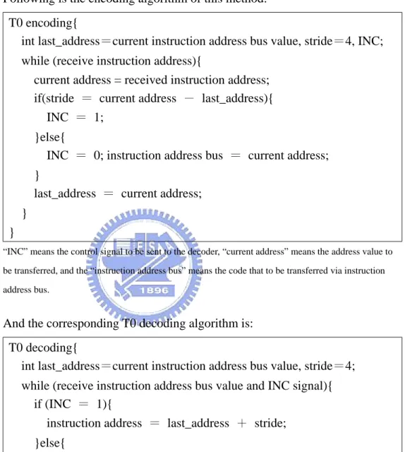
(19) BUS. The Figure 2.3.3 is a diagram of. encoder T0 encoding method:. INC. decoder. Figure 2.3.3: diagram of T0 Following is the encoding algorithm of this method: T0 encoding{ int last_address=current instruction address bus value, stride=4, INC; while (receive instruction address){ current address = received instruction address; if(stride = current address - last_address){ INC = 1; }else{ INC = 0; instruction address bus = current address; } last_address = current address; } } “INC” means the control signal to be sent to the decoder, “current address” means the address value to be transferred, and the “instruction address bus” means the code that to be transferred via instruction address bus.. And the corresponding T0 decoding algorithm is: T0 decoding{ int last_address=current instruction address bus value, stride=4; while (receive instruction address bus value and INC signal){ if (INC = 1){ instruction address = last_address + stride; }else{ instruction address = the instruction address bus value; } last_address = instruction address; } } “INC” means the control signal from the encoder, and the “instruction address” means the real address in this transmittion.. 9.
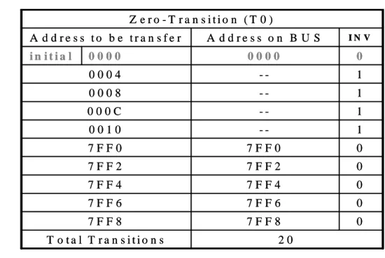
(20) The Figure 2.3.4 shows an example of the T0 Z e ro -T ra n s itio n (T 0 ) A d d re s s to b e tra n s fe r in itia l. A d d re ss o n B U S. IN V. 0000. 0000. 0. 0004. --. 1. 0008. --. 1. 000C. --. 1. 0010. --. 1. 7FF0. 7FF0. 0. 7FF2. 7FF2. 0. 7FF4. 7FF4. 0. 7FF6. 7FF6. 0. 7FF8. 7FF8. 0. T o ta l T ra n s itio n s. 20. Figure 2.3.4: Example of T0 Encoding The Figure 2.3.4 shows an easy example of T0 encoding. The initial bus value is ‘0000’, the bus width N=16, the stride applied here is 4, and the addresses to be transfer with time is listed in first column. In the first 4 transfers (‘0004’ ~ ’0010’), these values are all equal to last value plus 4, so the BUS is frozen and the INC is asserted while transferring these values in sequence. While transferring from ‘0010’ to ‘7FF0’, ‘7FF0’ must be transferred directly and INC must be de-asserted because (7FF0 – 0010)≠4. There are 12 transitions in this transfer, including 11 transitions on address bus and 1 transition on INC line. In the last 4 transfers (‘7FF2’ ~ ‘7FF8’), these value must be transferred through bus even if they are all in sequence. It is because that their stride (=2) do not equal to the stride applied by T0 in this example.. 10.
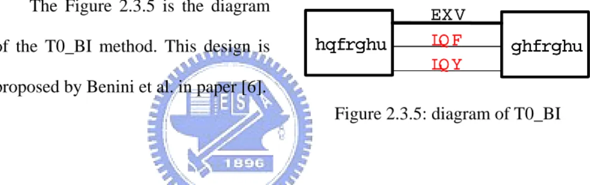
(21) 2.3.3 Combining T0 & BI (T0_BI) Thinking about the properties of BI (section 2.1) and T0 (section 2.2). The BI encoding method can only works well with randomly distributed data, and the T0 encoding method can only works well with sequential data. Because addresses on data bus may sometimes be accessed sequentially and randomly at the other time, combinations of the two encoding methods are required in order to get benefit of both the combined techniques. However, combination may result conflicts or confusions, and these problem should be resolved carefully.. The Figure 2.3.5 is the diagram of the T0_BI method. This design is. encoder. BUS IN C IN V. decoder. proposed by Benini et al. in paper [6]. Figure 2.3.5: diagram of T0_BI. The main idea of T0_BI design is using two separated control lines, INC and INV, to control the two functions, and the INC line is prior than the INV line. If the INC line is asserted, the BUS value is calculated by the INC function and the INV line is ignored. Else the INV line is treated as the control line of INV function.. 11.
(22) Following is the T0_BI encoding algorithm: T0_BI encoding{ int last_address=current data address bus value, stride=4, INC,INV; while (receive data address){ current address = received data address; if(stride = current address - last_address){ INC = 1; }else if(transition #>bus_width/2) { INC = 0; INV = 1; data address bus = inverted current address; }else{ INC = 0; INV = 0; data address bus = current address; } last_address = current address; } } Both “INC” and “INV” mean the control signals to be sent to the decoder, “current address” means the address value to be transferred, and the “data address bus” means the code that to be transferred via data address bus.. And the corresponding T0_BI decoding algorithm is: T0_BI decoding{ int last_address=current data address bus value, stride=4; while (receive data address bus value and INC, INV signals){ if (INC = 1){ data address = last_address + stride; }else if (INV = 1){ data address = inverted data address bus value; }else{ data address = the data address bus value; } last_address = data address; } } Both “INC” and “INV” mean the control signals from the encoder, and the “data address” means the real address in this transmittion.. 12.
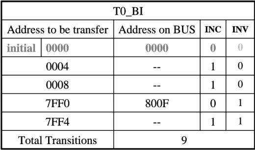
(23) The Figure 2.3.6 shows an example of the T0_BI. T0_BI Address to be transfer Address on BUS. INC. INV. 0000. 0. 0. 0004. --. 1. 0. 0008. --. 1. 0. 7FF0. 800F. 0. 1. 7FF4. --. 1. 1. initial 0000. Total Transitions. 9. Figure 2.3.6: Example of T0_BI Encoding The Figure 2.3.6 shows an easy example of T0_BI encoding. The initial bus value is ‘0000’, the bus width N=16, the stride applied here is 4, and the addresses to be transfer with time is listed in first column. In the first 2 transfers (‘0004’ ~ ’0008’), these values are all equal to last value plus 4, so the BUS is frozen and the INC is asserted while transferring these values in sequence. While transferring from ‘0008’ to ‘7FF0’, the Hamming distance from ‘0000’ to ‘7FF0’ is 11, larger than N/2, so that ‘7FF0’ is inverted to ‘800F’, the INV is asserted, and the INC is de-asserted. There are 7 transitions in this transfer, including 5 transitions on data address bus, 1 transition on INC line, and 1 transition on INV control lines. Next, while transferring from ‘800F’ to ‘7FF4’, because the real meaning is from ‘7FF0’ to ‘7FF4’ and ‘7FF4’ is equal to ‘7FF0’ plus 4, the BUS is frozen and the INC is asserted while transferring these values in sequence. Note that the INV line is still asserted because it is ignored here when the INC line is asserted. The total number of switching activities is 9.. 13.
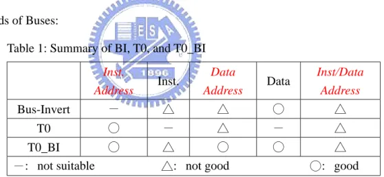
(24) 2.4 Summary & Observation Bus-Invert (BI) method inverts the transferring BUS value when it produces bit-transitions more than half of BUS width. An extra control line, called INV, is used to indicate which value is inverted. Zero-Transition (T0) method avoids the transfer of sequential addresses. An extra control line, called INC, is used to indicate which value is sequential to last address. T0_BI method, which combines both BI and T0 methods, uses two extra control signals, the INV and the INC, to control both two methods separately. However, these two control lines may result in many bit-transitions if functions switch frequently.. The following table shows the effect if applying these related works on 5 kinds of Buses: Table 1: Summary of BI, T0, and T0_BI. Bus-Invert. Inst. Address -. T0 T0_BI -: not suitable. △. Data Address △. ○. -. ○. △. Inst.. ○. Inst/Data Address △. △. -. △. ○. ○. △. △: not good. Data. ○: good. I think that there exists some improvement space in previous designs and new design issues for further study.. 1. Instruction Address Bus In T0 code, a discontinuous address breaks the consecution, and the address has to be sent explicitly to bus. This is the major restriction to the performance of T0 code. The sources of the discontinuous address are mainly come from branches, subroutine calls, and exception/interrupt handlings. Although the. 14.
(25) instructions are mostly sequential, branches still occurred frequently in common programs. The frequency of branch is ranged from about 10~20%, and strongly impact the result of T0 code. However, only few branches will change the target addresses. If the history taken branch targets are recored, it should be useful information while encoding.. 2. Data Address Bus First, the two control lines of T0_BI method may reduce to one control line to indicate both invert and sequential condition. Second, the stride value of data address may be replaced dynamically to meet the current data address stride. At last, the read and write data addresses usually have its individual continuity so as that it can be encoded separately to preserve the continuity.. 3. Instruction/Data Mixed Address Bus There are no previous design performs well on this Bus because of the continuity corruption of instruction and data address. I think that there are two design issues for encoding algorithms on this Bus: First, the instruction and data addresses own its individual continuity so that it can be encoded separately to preserve the continuity. Second, the data addresses are generated from load/store instructions. There should be some relationships between instruction and data address. The encoding method might make use of these relationships while encoding.. 15.
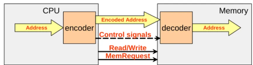
(26) 3 Designs My low-power address bus encoding schemes are described in this section. Section 3.1 will introduce the overview of my designs, section 3.2 to 3.4 will show the design details, and section 3.5 gives the design summary.. 3.1 Design Overview CPU. Memory Encoded Address. Address. encoder. Control signals. decoder. Address. Read/Write MemRequest. Figure 3.1: Address Bus Encoding Architecture Figure 3.1 shows my low-power address bus encoding architecture. The encoder gets addresses from CPU and outputs the encoded address and some control signals. Encoded addresses and control signals are transmitted to the decoder of memory. When the decoder receives encoded addresses and control signals, it converts this information into original data address. Two control lines, called Read/Write and MemRequest, are traditional memory control signals. Designs for instruction address bus, data address bus, and instruction/data mixed address bus will be explained in section 3.2~3.4. Following are brief descriptions of these designs: 1. Instruction Address Bus – recoding history branch targets as encoding information 2. Data Address Bus – using only 1 control line combining T0 and BI, adding Variable-Stride capability, and Preserving read/write continuities 3. Instruction/Data mixed Address Bus – preserving instruction/data continuities and making use of relationships between instruction and data address.. 16.
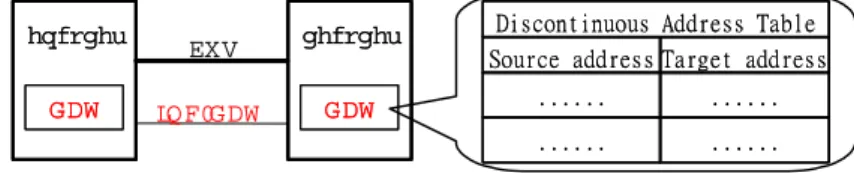
(27) 3.2 Instruction Address Bus Encoding: T0 with Discontinuous Address Table (T0 DAT) encoder DAT. BUS INC-DAT. decoder DAT. Discontinuous Address Table Source address Target address ....... ....... ....... ....... Figure 3.2.1: diagram of T0 DAT The Figure 3.2.1 shows the diagram of T0 with Discontinuous Address Table (DAT). The approach is based on T0 code, and adds a discontinuous address table (DAT) into both encoder and decoder to record the address pairs that are sent in sequence but with discontinuous values. Each entry of DAT records two values: “Source address” and “Target address”. “Source address” is equal to the address of branch instruction, and “Target address” is the target if branch taken. Afterward, this approach is called as “T0 DAT”. T0 DAT uses one control line, called INC-DAT, to control both DAT table and T0 function to transmit an instruction address sequence. First, the encoder of T0 DAT detects “DAT-hit” of the transferred address sequence. The “DAT-hit” means that the address pair (previous address, this address) exists in the DAT table. Transmission of an address with “DAT-hit” property is done with an asserted INC-DAT and a frozen address bus. If “DAT-hit” test fail, then the encoder checks to see if the to-be transferred address is consecutive to previous address and the previous address does not exist in the “Source address” field of DAT. Transmission of an address consecutive to previous address and the previous address does not exist in the “Source address” field of DAT is done with an asserted INC-DAT and a frozen address bus, too. Otherwise, the INC-DAT control line is de-asserted and the address is sent directly. Moreover, the discontinuous pair – “previous address. 17.
(28) and this address” is inserted into the DAT. After inserting into the DAT, this pair will be found in DAT in the future, and the next time the INC-DAT signal will be asserted if this address pair appears again. Following is the T0 DAT encoding algorithm: T0DAT encoding{ int last_address=current instruction address bus value, stride=4, INC-DAT; pair[] DAT; while (receive instruction address){ current address = received instruction address; if( pair(last_address, current address) found in the DAT) INC-DAT = 1; }else if(current address - last_address = stride && last_address does not exist in “Source Address” of DAT) { INC-DAT = 1; }else{ INC-DAT = 0; instruction address bus = current address; DAT.insert (last_address, current address); } last_address = current address; } } “INC-DAT” means the control signal to be sent to the decoder, “current address” means the address value to be transferred, and the “instruction address bus” means the code that to be transferred via instruction address bus.. 18.
(29) And the corresponding T0 DAT decoding algorithm is: T0DAT decoding{ int last_address=current instruction address bus value, stride=4; pair[] DAT; while (receive instruction address bus value and INC-DAT signal){ if (INC-DAT = 0){ instruction address = the instruction address bus value; DAT.insert (last_address, the instruction address bus value); }else if (last_address exists in “Source Address” of DAT){ instruction address = “Target Address” in that pair; }else{ instruction address = last_address + stride; } last_address = instruction address; } } “INC-DAT” means the control signal from the encoder, and the “instruction address” means the real address in this transmittion.. Note that the decoder interprets the meaning of the asserted INC-DAT line according to if the previous address exists in the “Source Address” field of DAT. If the encoder intends to transmit one consecutive address but the previous address happens to exist in the “Source Address” field of DAT, the decoder may erroneously interpret this as a discontinuous address pair. As a result, to avoid this error, the encoder simply sends the current address out directly. This situation might occur when leaving a loop, and the probability of this situation is much less than that of on-going loop. What have to be done is to take the precaution carefully.. 19.
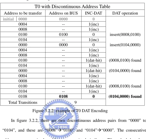
(30) Following is an example of T0 DAT. T0 with Discontinuous Address Table Address to be transfer initial 0000 0004 0008 0100 0104 0000 0004 0008 0100 0104 0000 0004 0008 0100 0104 0108 Total Transitions. Address on BUS 0000 --0100 -0000 ---------0108 9. INC-DAT 0 1(inc) 1(inc) 0 1(inc) 0 1(inc) 1(inc) 1(dat-hit) 1(inc) 1(dat-hit) 1(inc) 1(inc) 1(dat-hit) 1(inc) 0. DAT operation. insert(0008,0100) insert(0104,0000). (0008,0100) found (0104,0000) found. (0008,0100) found (0104,0000) found. Figure 3.2.2: example of T0 DAT Encoding In figure 3.2.2, there are two discontinuous address pairs from “0000” to “0104”, and these are “0008”Æ“0100” and “0104”Æ“0000”. The consecutive address sequences in the table are transmitted similar to T0 method, but these discontinuous address pairs are different treated here. While first transmission from “0008” to “0100”, “0100” is directly sent to the address bus and the INC-DAT line is de-asserted because “0100” is not sequential to “0008” and (0008, 0100) pair does not exist in DAT table. After transmission, the (0008, 0100) pair will be inserted into DAT table. When next time we meet “0008”Æ“0100” again, “0100” needn’t to be sent to the address bus because the (0008, 0100) pair is in the DAT. So the transmission of “0100” is just asserting the INC-DAT line. Similar operations will be occurred on “0104”Æ“0000”, and (0104, 0000) pair is added.. 20.
(31) Now we come to transmission from “0104” to “0108”. Thought “0108” is sequential to “0104”, “0108” has to be sent to the address bus to avoid the miss-understanding. Because the (0104, 0000) pair exists in the DAT table, if the encoder assert the INC-DAT line to mean that consecutive address is outputting, the decoder will miss-understand and get the “0000” as the transmitted address. Here, transitions of both address Bus and INC-DAT line are counted. There are totally 9 transitions in this example.. 21.
(32) 3.3 Data Address Bus Encoding Three versions of data address bus encoding scheme are proposed in this section, with the second and third built upon its predecessor version: 1. T0_BI_1 – combining T0 & BI using a single control line; 2. T0_BI_1/S – with Variable-Stride capability added; 3. T0_BI_1/S/RW – preserving read/write continuities in a multiplexed data address sequence.. 3.3.1 Combining T0 & BI using single control line (T0_BI_1) BUS. The Figure 3.3.1 shows the diagram. encoder of T0_BI_1 design.. INCV. decoder. Figure 3.3.1: diagram of T0_BI_1 T0_BI_1 design uses only one control line, called INCV, to control both INC and INV functions to transmit a data address, the encoder of T0_BI_1 first detects the continuity of the transferred address sequence. The continuity means that the current address is equal to the sum of the previous address and the stride. Transmission of an address with continuity property is done with an asserted INCV and a frozen address bus. If continuity test fails, then the encoder checks to see if the address pattern produces bus bit-transitions on more than half of the address bus lines and the inverted address pattern is not equal to the previous bus value (special cases), then the INCV is also asserted and the inverted address is sent over the address bus. Otherwise, the INCV line is de-asserted and the address will be sent directly. Upon activation, the decoder needs to identify the meaning of an asserted INCV line according to the received bus value. If the bus value is unchanged, the INCV line is interpreted as an “increment-by-stride” indicator. Otherwise, it is interpreted as an “invert” indicator. In this way, the single INCV 22.
(33) line can act as both INC and INV control signals, and address encoding still benefit from both BI and T0 schemes. Following is the T0_BI_1 encoding algorithm: T0_BI_1 encoding{ int last_address=current data address bus value, stride=4, INCV; while (receive data address){ current address = received data address; if(stride = current address - last_address){ INCV = 1; }else if(transition #>bus_width/2 && inverted address≠current data address bus value) { INCV = 1; data address bus = inverted current address; }else{ INCV = 0; data address bus = current address; } last_address = current address; } } “INCV” means the control signal to be sent to the decoder, “current address” means the address value to be transferred, and the “data address bus” means the code that to be transferred via data address bus.. And the corresponding T0_BI_1 decoding algorithm is: T0_BI_1 decoding{ int last_address=current data address bus value, stride=4; while (receive data address bus value and INCV signal){ if (INCV = 0){ data address = the data address bus value; }else if (the data address bus is frozen){ data address = last_address + stride; }else{ data address = inverted data address bus value; } last_address = data address; } } “INCV” means the control signal from the encoder, and the “data address” means the real address in this transmittion.. 23.
(34) Note that the decoder interprets the meaning of the asserted INCV line according to the received bus value. If the encoder intends to invert the bus value but the inverted value happens to equal the current bus value, the decoder may erroneously interpret this as a frozen address bus. As a result, to avoid this error, the encoder simply sends the current address out directly. I think that this is a very unlikely situation, but precaution must be carefully taken.. Following is an example of T0_BI_1. T0_BI_1 Address to be transfer Address on BUS. INCV. initial 0000. 0000. 0. 0004. 0004. 0. 0008. --. 1(inc). 7FF0. 800F. 1(inv). 7FF4. --. 1(inc). Total Transitions. 6. Figure 3.3.2: Example of T0_BI_1 The Figure 3.3.2 shows that transferring the same sequence in Figure 2.3.6. Compare with Figure 2.3.6, it is obviously that the major difference is that T0_BI uses two control signals but T0_BI_1 uses only one. The decoder of T0_BI_1 will not misunderstanding the meaning of encoder because that the T0 method always freezes the BUS while address are sequential.. 24.
(35) There are two special cases that should be concerned to avoid confusion in transfers via T0_BI_1 method. The Figure 3.3.3 shows examples of these two cases:. T0_BI_1 Address to be transfer Address on BUS. INCV. 000C. 000C. 0. 0010. --. 1 (inc). FFF3. 000C ÎFFF3. 1 (inv) Î0. (a): Special Case 1. T0_BI_1 Address to be transfer Address on BUS. INCV. 000C. FFF3. 1 (inv). 000C. FFF3 Î000C. 1 (inv) Î0. (b): Special Case2 Figure 3.3.3 Special Cases of T0_BI_1 In Figure 3.3.3a, the problem happens while transferring ‘FFF3’. In this case, if inverting ‘FFF3’ to ‘000C’, the decoder will misunderstand the meaning and use INC function to decode the value because the BUS value is un-changed. In Figure 3.3.3b, the problem happens while transferring ‘000C’. In this case, the first ‘000C’ has been inverted and transferred. If the second ‘000C’ is inverted, the decoder will misunderstand again. Both the two cases in Figure 3.3.3 have to force the value directly transferred through BUS in order not to make the decoder misunderstand the meaning of encoder, and will get the worst result, whose transition number (33) is equal to the 25.
(36) BUS width (32) plus 1, while address being transferred. Case 1 seldom happen because the probability of two sequential addresses with just inverted value is quite small. However, the Case 2 may happen easier for the reason that it will occur when two sequential addresses are equal, and here is one simple example: a[i] = a[i] + c, where a is an array and c is a constant value.. 26.
(37) 3.3.2 T0_BI_1 with Variable-Stride capability (T0_BI_1/S) Many data are structured (arrays, matrices, etc.), and accesses to such structured data have very predictable data addresses. The term “stride” is used to describe the byte offset between consecutive access addresses of this kind. Two factors affect the stride value: one is the data item size (64 bits for scientific data, 32 bits for general-purpose computing, and 16 or 8 bits for multimedia applications). The other is the access pattern (column, row, diagonal, …) interacted with the storage scheme (row-major, column-major, others). These complicate the stride value computation and identification; different stride values may even mix in the code sequence. Here the changing stride problem is dealt with. Interleaved stride problem will be tackled in next section.. encoder Last Address Applied Stride New Stride logics. decoder BUS INCV. Last Address Applied Stride New Stride logics. Figure 3.3.4: diagram of T0_BI_1/S The major goal of variable-stride capability is to make the stride applied by T0 changes with the behavior of data address sequence in order to fit the actual stride of data address. Figure 3.3.4 shows the main idea of T0_BI_1 with Variable-Stride Capability added in. First, the chosen stride is applied by T0 method while transferring addresses. Second, the candidate stride is modified when current address stride is not equal to chosen stride. After the candidate stride matures, it is used to replace the chosen stride. At last, how to make the candidate stride mature? Setting an endurance value (e) as a method parameter, which means that the candidate stride will be applied if it appears e times continuously.. Following is the T0_BI_1/S encoding algorithm, in which italic and 27.
(38) underlined contents are newly added: T0_BI_1/S encoding{ int last_address=current data address bus value; int chosen_stride=4, INCV, e; while (receive data address){ current address = received data address; if(chosen_stride = current address - last_address){ INCV = 1; }else if(transition # > bus_width/2 && inverted address≠current data address bus value) { INCV = 1; data address bus = inverted current address; }else{ INCV = 0; data address bus = current address; } If (the new stride appears e time continuously) chosen_stride = current address - last_address; last_address = current address; } } “INCV” means the control signal to be sent to the decoder, “current address” means the address value to be transferred, and the “data address bus” means the code that to be transferred via data address bus. Variable-Stride Capability uses “current_stride” and endurance “e” to dynamically change the stride value depend on the behavior of current data address sequence.. 28.
(39) And the corresponding T0_BI_1/S decoding algorithm, in which italic and underlined contents are newly added, is: T0_BI_1/S decoding{ int last_address=current data address bus value, chosen_stride=4, e; While (receive data address bus value and INCV signal){ if (INCV = 0){ data address = the data address bus value; }else if (the data address bus is frozen){ data address = last_address + chosen_stride; }else{ data address = inverted data address bus value; } If (the new stride appears e time continuously) chosen_stride = data address - last_address; last_address = data address; } } “INCV” means the control signal from the encoder, and the “data address” means the real address in this transmittion. Variable-Stride Capability uses “current_stride” and endurance “e” to dynamically change the stride value depend on the behavior of current data address sequence.. The above algorithms are very simple and straight forward methods, and work only with array accesses without any intervening data accesses. Nevertheless, with these simple ideas as the basis, many innovative schemes can be derived, such as the one to be introduced next.. 29.
(40) Following is an example of T0_BI_1/S method and the endurance=1.. T0_BI_1 Address to be transfer Address on BUS initial 0000. INCV. 0000. 0. 0004. --. 0. 0008. --. 1 (inc). 7FF0. 800F. 1 (inv). 7FF2. 800D. 1 (inv). 7FF4. 800B. 1 (inv). Total Transitions. 9 (a): T0_BI_1. T0_BI_1/S, endurance = 1 Address to be transfer. current Address INCV chosen (candidate) on BUS stride Stride. init 0000. 0. 0. 0000. 0. 0004. 0. 4. 0004. 0. 0008. 4. 4. --. 1 (inc). 7FF0. 4. 7FE8. 800F. 1 (inv). 7FF2. 7FE8. 2. 800D. 1 (inv). 7FF4. 2. 2. --. 1 (inc). Total Transitions. 7. (b): T0_BI_1/S, endurance = 1 Figure 3.3.5: Example of T0_BI1/S, endurance=1. 30.
(41) There are two additional column (‘chosen stride’ & ‘current stride’) in Figure 3.3.5b. The chosen stride means the stride that Variable-Stride ability chooses now, and the current stride is the stride value while transferring. Because the candidate stride is always replaced by current stride, they are presented in one column. The most important thing here is that the chosen stride is changed dynamically to fit the data address stride. In order to make it convenient in later discussion, there are some notations used in this paper. . FS#: meaning Fixed-Stride, whose stride is equal to # ex: FS4-Fixed-Stride with stride=4. . VS#: meaning Variable-Stride, whose endurance is equal to # ex: VS1-Variable-Stride, endurance=1, which is used in previous example.. 31.
(42) 3.3.3 Preserving Read/Write Continuities in a multiplexed data address sequence (T0_BI_1/S/RW) Data memory are read and written by the CPU, both over the same set of address and data buses. While data read sequence and write sequence each has its own stride characteristics, these stride characteristics are unfortunately torn apart and severely contaminated due to the intervention of the read/write address sequences in a single address trace. How to preserve and utilize the individual read and write stride characteristics in bus encoding hence becomes an interesting problem. As a result, if the read and write address sequences can be individually encoded , it must gain more power savings. Figure 3.3.6 shows the T0_BI_1/S/RW block diagram. In this modification, the read/write control line, which exists in all memory systems, is used to indicate the address being a read or write address. With this, each of the read and write address sequences can be separately encoded using the variable stride T0_BI_1/S method.. Data Address. R/W. CPU encoder. Encoded Address. Read Write stride stride LastAddr LastAddr. INCV Read/Write enable. endurance endurance. logic. logic. Memory decoder Read Write stride stride LastAddr LastAddr endurance endurance. logic. logic. Figure 3.3.6 T0_BI_1/S/RW block diagram. 32. Data Address.
(43) Following is the T0_BI_1/S/RW encoding algorithm, in which italic and underlined contents are newly added: T0_BI_1/S/RW encoding{ int INCV, R_e, W_e; int R_last_address=current data address bus value; int W_last_address=current data address bus value; int R_chosen_stride=4, W_chosen_stride=4; while (receive data address and RW signal){ current address = received data address; if ( (RW=1 && R_chosen_stride=current address - R_last_address) || (RW=0 && W_chosen_stride=current address - W_last_address) ){ INCV = 1; }else if(transition # > bus_width/2 && inverted address≠current data address bus value) { INCV = 1; data address bus = inverted current address; }else{ INCV = 0; data address bus = current address; } if(RW=1){ If (the new stride appears e time continuously) R_chosen_stride = current address - R_last_address; R_last_address = current address; }else{ If (the new stride appears e time continuously) W_chosen_stride = current address - W_last_address; W_last_address = current address; } } } “INCV” means the control signal to be sent to the decoder, “current address” means the address value to be transferred, and the “data address bus” means the code that to be transferred via data address bus. Terms start with “R_” or “W_” are duplicated registers needed for Preserving Read/Write Sequence.. 33.
(44) And the corresponding T0_BI_1/S/RW decoding algorithm, in which italic and underlined contents are newly added, is: T0_BI_1/S/RW decoding{ int R_e, W_e; int R_last_address=current data address bus value; int W_last_address=current data address bus value; int R_chosen_stride=0, W_chosen_stride=0; while(receive data address bus value and INCV signal and RW signal){ if (INCV = 0){ data address = the data address bus value; }else if (the data address bus is frozen){ if (RW=1) data address = R_last_address + R_chosen_stride; else data address = W_last_address + W_chosen_stride; }else{ data address = inverted data address bus value; } if(RW=1){ If (the new stride appears e time continuously) R_chosen_stride = data address - R_last_address; R_last_address = data address; }else{ If (the new stride appears e time continuously) W_chosen_stride = data address - W_last_address; W_last_address = data address; } } } “INCV” means the control signal from the encoder, and the “data address” means the real address in this transmittion. Terms start with “R_” or “W_” are duplicated registers needed for Preserving Read/Write Sequence.. 34.
(45) 3.4 Instruction/Data Mixed Address Bus Encoding CPU Inst Address Data Address. Memory M U X. Inst/Data Address. Inst/Data Address. Read/Write MemRequest. Figure 3.4.1: diagram of general instruction/data mixed address bus Figure 3.4.1 shows the diagram of general instruction/data mixed address bus. CPU multiplex the instruction address stream and data address stream into one stream, and transfer this stream via instruction/data mixed address bus. Two control lines, called Read/Write and MemRequest, are traditional memory control signals. In my design for instruction/data mixed address bus, encoder/decoder is added into CPU/memory. The encoder separately receives two address streams: instruction address stream and data address stream, and transmit the encoded address to the decoder in the memory. The decoder has to output the original addresses to the memory. Needed decoding information may be sent through some extra control signals. Figure 3.4.2 is the diagram of my instruction/data mixed address bus encoding. CPU. Memory. Inst Address. Encoded Address. encoder Data Address. Control signals. decoder. Inst/Data Address. Read/Write MemRequest. Figure 3.4.2: diagram of my instruction/data mixed address bus encoding Two versions of instruction/data mixed address bus encoding scheme are proposed in this section, with the second built upon its predecessor version: 1. I/D Selector – preserving instruction/data continuities in a multiplexed address sequence 2. Stride-Table – Applying different stride value on each data access 35.
(46) 3.4.1 Preserving Instruction/Data Continuities in a multiplexed address sequence (I/D Selector) In “2 Buses” architecture, both instruction and data transmitted over the same set of address and data buses. While instruction sequence and data access sequence each has its own stride characteristics, these stride characteristics are unfortunately torn apart and severely contaminated due to the intervention of the instruction/data address sequence in one single address trace. How to preserve and utilize the individual instruction and data access stride characteristics in bus encoding hence becomes an interesting problem. As a result, if the instruction and data address sequences can be encoded individually, it must gain more power savings. Figure 3.4.3 shows the “I/D selector” block diagram. In this modification, the extra read/write control line is used to indicate the address being a instruction or data address. With this, each of the read and write address sequences can separately be encoded using methods suitable for them. encoder I. D. DAT. ?. BUS INC-DAT I/D selector. decoder I. D. DAT. ?. Figure 3.4.3: diagram of I/D selector Here two encoding methods are needed, one for instruction address sequence and one for data address sequence. For the instruction address sequence, the “T0 DAT” proposed in section 3.2 should be good enough because it avoid the transmission of both consecutive address sequence and regular taken branch target addresses. For the data address sequence, the “T0_BI_1/S/RW”cproposed in section 3.3 could also be applied here. However, this method does not make use of the relationships between instruction and data address. I will propose one new. 36.
(47) design, called “Stride-Table”, to make use of these relationships and reduce more bus transitions.. 3.4.2 Applying different stride value on each data access (Stride-Table) Data addresses are resulted from load/store instructions, and each load/store instruction usually generates consecutive address sequence when it is executed more than once. While data access of each load/store instruction has its own stride characteristics, these stride characteristics are unfortunately torn apart and severely contaminated due to the intervention of these data accesses in a single data address trace. How to preserve and utilize the stride characteristics of data access of each load/store instruction hence becomes an interesting problem. As a result, if individual stride value is applied for data access of each load/store instruction, more power saving must be gained. How to tell which load/store instruction is executed in the instruction/data mixed address bus? The main idea is that because the data access is resulted by execution load/store instruction, the last instruction address before this data access should be the address of load/store instruction. Even if taking the pipelining effect of CPU, the real address of load/store instruction should equal to the last instruction address minus an offset value. As a result, I take the last instruction address before data access as the key information of telling which load/store instructions is executed in this design. encoder I. D. DAT Stride Table. BUS INC-DAT/ST I/D selector. decoder I. D. DAT Stride Table. Stride Table Index Address. Applied Stride. Last Address. ....... ....... ....... ....... ....... ....... Figure 3.4.4: diagram of I/D selector with T0 DAT and Stride-Table 37.
(48) The Figure 3.4.4 shows the diagram of I/D selector with T0 DAT and Stride-Table. This approach adds a “Stride Table” into both encoder and decoder. Each entry of Stride-Table records three values: “Index Address”, “Applied Stride”, and “Last Address”. The “Index Address” records the address of last instruction address before data access; the “Applied Stride” records the stride value to be applied when executing this load/store instruction; the “Last Address” records the data address accessed by the load/store instruction last time. Moreover, one control signal, called ST, is required to indicate which address is not transmitted on the bus but the decoder could calculate the address by information in the Stride-Table. Here, this control signal can be combined with the INC-DAT line of T0 DAT method. How this approach works? While transferring the instruction addresses, the I/D Selector is asserted and T0 DAT method works as if it is applied in the instruction address bus. Besides this, the encoder will memorize the latest instruction address in mind, and so do the decoder. When one data address arrives, the I/D selector will be de-asserted and the encoder uses the latest instruction address as index value to access the Stride-Table. If there is one entry whose “Index Address” is equal to the latest instruction address, the encoder will get the “Applied Stride” and “Last Address” of this load/store instruction. Depending on the to-be transferred data address is equal to “Last Address”+“Applied Stride” or not, the encoder decides to assert ST line and freeze the bus or de-assert ST line and transmit this data address directly via bus. After that, the “Applied Stride” and “Last Address” of this entry will be updated. If there is no entry whose “Index Address” is equal to the latest instruction address, the encoder has to de-assert ST line, transmit this data address directly via bus, and insert one entry (latest instruction address, default stride, this data address) into 38.
(49) Stride-Table. (The default stride is 4 in my design.) While the decoder receiving address transfer with de-asserted I/D signal, actions differ depending on the ST signal. If the ST line is asserted, the decoder uses the latest instruction address as index value to access the Stride-Table and gets the “Applied Stride” and “Last Address” for this data access. The original data address equals to “Last Address"+“Applied Stride”. Otherwise, the decoder receives data address directly from the bus. After this data address transmission, decoder has to insert one entry (latest instruction address, default stride, this data address) into Stride-Table if no entry whose “Index Address” is equal to the latest instruction address, or update the “Applied Stride” and “Last Address” otherwise. Following is an example of I/D Selector with T0 DAT and Stride-Table: Addresses leading with “I” mean instruction addresses, and “D” for data addresses. Address trace of 3 iterations of a simple loop are listed here.. I D I I D I D I I D I I I I I. Address Sequence 20 I 20 I 20 600 D 604 D 608 24 I 24 I 24 28 I 28 I 28 100 D 104 D 108 32 I 32 I 32 400 D 396 D 392 36 I 36 I 36 40 I 40 I 40 900 D 898 D 896 44 I 44 I 44 48 I 48 I 48 52 I 52 I 52 56 I 56 I 56 60 I 60 I 60. DAT Source Address. Target Address. Stride Table Index Address. Applied Stride. Last Address. red&italic: bus frozen black: transmit value Figure 3.4.5: example of I/D Selector with T0 DAT and Stride-Table, At Start. 39.
(50) Figure 3.4.5 shows a snapshot at start. The DAT and Stride-Table are both empty at this time.. Snapshot of first iteration:. I D I I D I D I I D I I I I I. Address Sequence 20 I 20 I 20 600 D 604 D 608 24 I 24 I 24 28 I 28 I 28 100 D 104 D 108 32 I 32 I 32 400 D 396 D 392 36 I 36 I 36 40 I 40 I 40 900 D 898 D 896 44 I 44 I 44 48 I 48 I 48 52 I 52 I 52 56 I 56 I 56 60 I 60 I 60. DAT Source Address. Target Address. Stride Table Index Applied Last Address Stride Address. red&italic: bus frozen black: transmit value. 20. 4. 600. 28. 4. 100. 32. 4. 400. 40. 4. 900. Figure 3.4.6: example of I/D Selector with T0 DAT and Stride-Table, Iteration 1 In the first iteration, all instruction addresses are consecutive and need not to be transmitted via bus except the first one. Data addresses are transmitted directly via bus because there are no information in Stride-Table at start. These data addresses and its previous instruction address are inserted into Stride-Table with default stride value = 4.. 40.
(51) Snapshot of second iteration:. I D I I D I D I I D I I I I I. Address Sequence 20 I 20 I 20 600 D 604 D 608 24 I 24 I 24 28 I 28 I 28 100 D 104 D 108 32 I 32 I 32 400 D 396 D 392 36 I 36 I 36 40 I 40 I 40 900 D 898 D 896 44 I 44 I 44 48 I 48 I 48 52 I 52 I 52 56 I 56 I 56 60 I 60 I 60. DAT Source Address. Target Address. 60. 20. Stride Table. red&italic: bus frozen black: transmit value. Index Address. Applied Stride. Last Address. 20. 4. 600 604. 28. 4. 100 104. 32. -4 4. 400 396. 40. -2 4. 900 898. Figure 3.4.7: example of I/D Selector with T0 DAT and Stride-Table, Iteration 2 In the second iteration, the discontinuous address pair (60, 20) is inserted into DAT. All instruction addresses except “20” need not to be transmitted via bus, too. Data addresses “604” & “104” meet the default stride value so that the bus is frozen and the INC-DAT/ST line is asserted. Data addresses “396” & “898” do not meet the default stride value so that the two addresses have to transmitted via bus. The decoder updates “Applied Stride” and “Last Address” of the corresponding entry for further transfer.. 41.
(52) Snapshot of third iteration:. I D I I D I D I I D I I I I I. Address Sequence 20 I 20 I 20 600 D 604 D 608 24 I 24 I 24 28 I 28 I 28 100 D 104 D 108 32 I 32 I 32 400 D 396 D 392 36 I 36 I 36 40 I 40 I 40 900 D 898 D 896 44 I 44 I 44 48 I 48 I 48 52 I 52 I 52 56 I 56 I 56 60 I 60 I 60. DAT Source Address. Target Address. 60. 20. Stride Table. red&italic: bus frozen black: transmit value. Index Address. Applied Stride. Last Address. 20. 4. 600 604 608. 28. 4. 100 104 108. 32. -4 4. 400 396 392. 40. -2 4. 900 898 896. Figure 3.4.8: example of I/D Selector with T0 DAT and Stride-Table, Iteration 3 In the third iteration and further iterations, all instruction and data addresses do not need to be transmitted via bus. Transmissions of these addresses are just asserting INC-DAT/ST line and switching I/D Selector line respect. This situation will be held until leaving the loop. Though Stride-Table avoids the transmission of regular data access, there are still some data addresses will be transmitted via bus. While transmitting these data addresses, Bus-Invert could be added for additional power saving. The combination of Stride-Table and Bus-Invert is shown as diagram in Figure 3.4.9:. encoder. BUS. decoder. I. D. INC-DAT/ST-INV. I. D. DAT. ST. I/D selector. DAT. ST. Figure 3.4.9: diagram of Stride-Table combining with Bus-Invert 42.
(53) The INV control line required for Bus-Invert method is combined with INC-DAT/ST line using similar approach mention in section 3.3.1. The keys to identify the meaning of an asserted INC-DAT/ST-INV control line are “I/D Selector” status and bus frozen or not.. 3.5 Summary T0 DAT make use of history branch target to avoid transfer of both regular taken branch target address and consecutive address sequence. T0_BI_1/S/RW uses only one control signal controls both BI and T0, dynamically changing applied stride value, and encoding read/write sequence individually. I/D Selector with T0 DAT and Stride-Table preserves continuity of both inst and data address, and make use of relationship between inst and data. These three designs are respectively suitable for instruction address bus, data address bus, and instruction/data mixed address bus. The effect of my designs will be shown in next section.. 43.
(54) 4 Simulation I implement my designs using simulation, and use benchmarks to validate these designs. The target embedded system conforms to a portable personal multimedia/ communication device, and the test programs are selected accordingly. The performance metric is the ratio of reduced data address bus bit toggles. To simplify the result, only overall performance improvements are reported. Although readers may be interested in the effects of each individual technique and their incremental effects on top of other techniques, these data are not shown here due to page limits.. 4.1 Simulation Environment The simulated embedded system platform assumptions are listed below: 1.. The processor is ARM7TDMI, and there is only one processor in the system.. 2.. The memory is separated into two parts: instruction memory, and data memory.. 3.. There is no cache memory.. 4.. All instructions are compiled in ARM mode. There are four types of benchmarks, and each type has 2 programs in it. These. benchmark programs are selected from MediaBench, a popular benchmark suite including multi-media and communication applications. These benchmarks are: 1.. ADPCM Description: ADPCM stands for Adaptive Differential Pulse Code Modulation. It is a family of speech compression and decompression algorithms. A common implementation takes 16-bit linear PCM samples and converts them to 4-bit samples, yielding a compression rate of 4:1. The ADPCM code used is the Intel/DVI ADPCM code which is being recommended by the IMA Digital Audio Technical Working Group.. 44.
(55) 2.. EPIC Description: EPIC (Efficient Pyramid Image Coder) is an experimental image data compression utility written in the C programming language. The compression algorithms are based on a biorthogonal critically-sampled dyadic wavelet decomposition and a combined run-length/Huffman entropy coder. The filters have been designed to allow extremely fast decoding on conventional (ie, non-floating point) hardware, at the expense of slower encoding and a slight degradation in compression quality (as compared to a good orthogonal wavelet decomposition).. 3.. GSM Description: As part of this effort we are publishing an implementation of the European GSM 06.10 provisional standard for full-rate speech transcoding, prI-ETS 300 036, which uses RPE/LTP (residual pulse excitation/long term prediction) coding at 13 kbit/s. GSM 06.10 compresses frames of 160 13-bit samples (8 kHz sampling rate, i.e. a frame rate of 50 Hz) into 260 bits; for compatibility with typical UNIX applications, our implementation turns frames of 160 16-bit linear samples into 33-byte frames (1650 Bytes/s). The quality of the algorithm is good enough for reliable speaker recognition; even music often survives transcoding in recognizable form (given the bandwidth limitations of 8 kHz sampling rate).. 4.. JPEG Description: This package contains C software to implement JPEG image compression and decompression. JPEG (pronounced "jay-peg") is a standardized compression method for full-color and gray-scale images. JPEG is intended for compressing "real-world" scenes; line drawings, cartoons and other non-realistic images are not its strong suit. JPEG is lossy, meaning that 45.
(56) the output image is not exactly identical to the input image.. Benchmarks. ARM7 TDMI. Trace. Simulator. Result Figure 4.1: Simulation flowchart Figure 4.1 shows the flowchart of simulation. The benchmarks are run in the ARM-Emulator7t, and the emulator dumps the trace of program execution. After that, a simulator takes the trace as input and counts the number of bus bit transitions.. 46.
(57) 4.2 Simulation Results The goal of address bus encoding methods is to reduce the transitions on address bus, so the result of encodings will be presented as percentage of reduced transitions, which is calculated as (% of Reduced Transitions) = (Reduced Transitions) ÷ (unencoded Transitions). The higher this value is, the more effective the corresponding design.. 4.2.1 Results of Instruction Address Bus Encoding Figure 4.2.1 shows the effects of different DAT size: audio. epic. toast. jpeg. Average. 100% % of Reduced Transition. 95% 90% 85% 80% 75% 70% 65% 60% 1. 2. 4. 8. 16 32 DAT Size. 64. 128. 256. ∞. Figure 4.2.1: effects of DAT size In this figure, two DAT sizes are chosen. The first one is size=4, it gets good performance for most applications. If viewing T0 DAT with infinite size as optimal case, it is 97.6% of the optimal case. The second one is size=32, it satisfies all applications in the applied benchmarks, and is 99.8% of optimal case.. 47.
(58) T0. DAT(4). DAT(32). % of Reduced Transitions. 100% 95% 90% 85% 80% 75% 70% 65% 60% audio. epic. toast. jpeg. Average. Figure 4.2.2: Results of T0 DAT In figure 4.2.2, we can see that averagely T0 DAT(4) achieves 88.7% reduction of the original bit transitions, which is 6.2% more than the T0 method can do. T0 DAT(32) achieves 90.5% reduction of the original bit transitions, which is 8.1% more than the T0 method can do.. 4.2.2 Results of Data Address Bus Encoding Figure 4.2.3 shows the simulation results of T0_BI_1/S/RW method.. BI. % of Reduced Transitions. 35%. T0. 32.0%. T0_BI. T0_BI_1/S/RW. 30.8%. 30%. 26.0%. 25% 20.1%. 21.3%. 20.0% 20.7%. 20% 15% 10% 5%. 9.4%. 9.2%. 7.8% 4.1%4.7%. 11.5%. 11.2%. 9.7% 4.6%. 2.4%. 2.9%. 0.6%. 0.6%. 0% audio. epic. toast. jpeg. Figure 4.2.3: Results of T0_BI_1/S/RW 48. Average.
(59) In figure 4.2.3, the newly proposed T0_BI_1/S/RW method achieves 26% reduction of the original bit transitions. Comparing with T0_BI method, it reduces 14.5% transitions more than T0_BI method.. 4.2.3 Results of Inst/Data mixed Address Bus Encoding Figure 4.2.4 shows the effects of different Stride-Table size:. % of Reduced Transitions. audio. epic. toast. jpec. Average. 100% 90% 80% 70% 60% 50% 40% 1. 2. 4. 8. 16. 32 64 128 StrideTable Size. 256. 512 1024 ∞. Figure 4.2.4: effects of Stride-Table Size In this figure, two Stride-Table size are chosen, too. The first choice is size= 32, it gets good performance for more than half applications in the applied benchmarks. If viewing Stride-Table size with infinite size as optimal case, it is 91.4% of the optimal case. The second choice is size=128, it satisfies all applications in the applied benchmarks, and is 99% of optimal case.. 49.
(60) T0-BI. T0DAT-T0 BI 1/S/RW. T0DAT-ST(32). T0DAT-ST(128). T0DAT-STINV(128). % of Reduced Transitions. 100% 90% 80% 70% 60% 50% 40% audio. epic. toast. jpec. Average. Figure 4.2.5: Results of I/D Selector with T0 DAT and Stride-Table In figure 4.2.5, it’s easy to find that I/D Selector with T0 DAT and Stride-Table(32) achieves 70.8% transition reduction of the un-encoded bus, which is 24.7% more than T0_BI method and 7.5% more than that of I/D Selector with T0 DAT and T0_BI_1/S/RW. I/D Selector with T0 DAT and Stride-Table(128) achieves 77.4% transition reduction of the un-encoded bus, which is 33.8% more that T0_BI method and 16.6% more than that of I/D Selector with T0 DAT and T0_BI_1/S/RW.. 50.
(61) 5 Conclusions In my thesis, I study the low-power address bus encoding techniques. First, T0 DAT method is proposed for instruction address bus. It avoids transmission of both consecutive addresses and regular taken branch targets. Compared with the T0 method, T0 DAT achieves 90.5% reduction of the original bit-transitions, 8.1% more than the T0 method. Second, T0_BI_1/S/RW method is proposed for data address bus. It integrates T0 and BI methods using only one control line, introduces a variable-stride methods which deals with dynamically changing strides, and preserves the continuities of read and write addresses using separated sets of encoding information. Compared with the T0_BI method, my design achieves 26% reduction of the original bit transitions, 14.5% more than the T0_BI method. Lastly, I propose one encoding method for instruction/data mixed address bus. It preserves the individuality of instruction and data address, and applies strides for each load/store instruction. Compared with the T0_BI method, my design achieves 77.4% reduction of the original bit transitions, 33.8% more than the T0_BI method. The simulation results show that my address bus encoding methods have much less bit transitions. To make the power estimation results more precise, a bus power model needs to be carefully constructed. And the hardware overheads for the additional control lines/logic, include silicon area, delay, and power, also need to be evaluated.. 51.
(62) 6 References [1] S. Wuytack, F. Catthoor, L. Nachtergaele, H. De Man, “Global communication and memory optimizing transformati ons for low power signal processing systems,” IWLPD-94: ACM/IEEE International Workshop on Low Power Design, Apr. 1994, pp. 203-208. [2] C. L. Su, C. Y. Tsui, A. M. Despain, “Saving Power in the Control Path of Embedded Processors,” IEEE Design and Test of Computers, Vol. 11, No. 4, pp. 24-30, Winter 1994 [3] Y. Aghaghiri, F. Fallah, and M. Pedram, “Irredundant address bus encoding for low-power,” in Proc. IEEE Int. Symp. Low-Power Electronics and Design, Aug. 2001, pp. 182–187. [4] M. R. Stan and W. P. Burleson, “Bus-invert coding for low-power I/O,” IEEE Transactions on VLSI Systems, Vol. 3, No. 1, pp. 49-58, 1995 [5] L. Benini, G. DeMicheli, E.Macii, D. Sciuto, and C. Silvano, “Asymptotic zero-transition activity encoding for address busses in low-power microprocessor-based systems” GLS-VLSI-97: IEEE 7th Great Lakes Symposium on VLSI,pp. 77-82, Urbanana-Champaign, IL, March 1997. [6] L. Benini, G. DeMicheli, E.Macii, D. Sciuto, and C. Silvano, “Address bus encoding techniques for system-level power optimization,” Proc. Of Design Automation and Test in Europe, pp. 861-866, Feb. 1998. 52.
(63) 問題討論 問題一:一般 BUS 傳送資料之前已將 data 與上一筆做 XOR;應加入考慮! 答: 一般來說, XOR 的的方法如下圖所示:. 在傳送 data pattern 時,將它與上一筆 data pattern 做 xor 之後再傳送到 BUS 上, 而接收端則將收到的資料與上一次解開的 data pattern 再做一次 xor 得到傳送的資 料。 此一方法能夠減少有連續特性的資料(如 instruction address)傳輸時所產生的 bit-transitions,同時也不會增加一直傳送同一筆資料(bus frozen)時的 bit-transition; 對於 random distributed 的資料則影響不大。而本論文設計的方法,是針對 instruction address bus、data address bus、以及 instruction/data mixed address bus 上可利用的連續 性所設計,儘量將傳送的 pattern 藉由 decoder 計算出來,將 BUS frozen 以避免不必 要的 bit-transitions。因此,只要將本論文中設計的方法,encoder 放在 XOR encoder 之前,decoder 放在 XOR decoder 之後,就可以正確傳送,同時能夠利用 XOR encoder/decoder 進一步減少 BUS 上的 bit-transition 數。. 53.
數據
+7
相關文件
• The memory storage unit is where instructions and data are held while a computer program is running.. • A bus is a group of parallel wires that transfer data from one part of
A constant offset is added to a data label to produce an effective address (EA) The address is dereferenced to get effective address (EA). The address is dereferenced to get
• The memory storage unit holds instructions and data for a running program.. • A bus is a group of wires that transfer data from one part to another (data,
(B)Data Bus 是在 CPU 和 Memory 之間傳送資料,所以是雙向性 (C)Address Bus 可用來標明 Memory 或 I/O Port 位址的地方 (D)Data Bus 的長度和 Address
其功能是列出系統的 ARP Table,以及設定及 刪除 ARP
經由 PPP 取得網路IP、Gateway與DNS 等 設定後,並更動 Routing Table,將Default Gateway 設為由 PPP取得的 Gateway
Return address Local variables Previous frame pointer?. Return address
• Last data pointer stores the memory address of the operand for the last non-control instruction. Last instruction pointer stored the address of the last
