Size-dependent
field-emission characteristics of ZnO nanowires grown by porous
anodic aluminum oxide templates assistance
Chun-Hung Lai
a,⁎
, Chia-Wei Chang
b, Tseung-Yuen Tseng
ca
Department of Electronic Engineering, National United University, Miaoli 360, Taiwan
bEtron Technology, Inc., No. 6, Technology Road 5, Hsinchu Science Park, Hsinchu 30078, Taiwan c
Department of Electronics Engineering, National Chiao Tung University, Hsinchu 300, Taiwan
a b s t r a c t
a r t i c l e i n f o
Available online 6 May 2010 Keywords:
Field-emission Hydrothermal Template
Field enhancement factor
Thefield-emission electrical properties of hydrothermally synthesized zinc-oxide nanowires grown on SiO2– Si substrate are reported. Vertically aligned single-crystalline emitters with distinct length L and diameter D are realized by controlling the assisted growth of porous anodic aluminum oxide (AAO) templates. Field-emission measurement revealed that thesefield emitters exhibited controllable turn-on field Etoand the field enhancement factor β. Sample with feature size of L=500 nm and D=80 nm was prepared and then used as a basis for examining the size effect. Lower Etoand higherβ were observed consistently for increasing the aspect ratio L/D. The enhanced properties of Eto= 1.48 V/μm and β up to 6100 are achieved for L/D=53 (L = 1600 nm and D = 30 nm). Optimal characterizing parameters of Eto and β will be reached while pursuing extreme L/D practically. Factors such as the geometric limit of AAO template manufacture and the filling efficiency of ZnO into AAO pores will exert influence on the size-dependent effect.
© 2010 Elsevier B.V. All rights reserved.
1. Introduction
Zinc oxide nanowires (NWs) are promising semiconductor materials for applications in photonic and electronic devices, such as dye-sensitized solar cells[1], varistors[2], photodiodes[3], nanolasers [4], and gas sensors[5]. In addition, ZnO NW array has been proved to be a viable alternative as afield emitter due to its peculiar properties of oxide resistibility and high chemical stability, as compared to carbon nanotubes (CNTs). For emitter application, the turn-onfield Eto
and the field enhancement factor β are two dominant parameters characterizing the emission efficiency. Some effective methods, such as plasma bombardment[6], thermal annealing, or metal element doped[7], are adopted desirably to achieve highest current density at
lower onset voltage [8]. Topics in focus are on examining
the morphological variations based on various ZnO nanostructures [9–13], geometrical factors like the areal density of NWs and the distance between emitters and anode are also investigated[14,15]. However, studies on the influence of the emitter's aspect ratio are rare due to the difficulty in growth controllability, especially for ZnO NWs. Growth of ZnO nanostructures can be obtained by vapor–liquid– solid method (VLS)[16], metal–organic chemical vapor deposition (MOCVD) [17], and thermal evaporation [18]. In this paper, we demonstrated the hydrothermal process in aqueous solution at temperatures below 100 °C[19], and then grew the NWs by porous
anodic aluminum oxide (AAO) template without use of seeding layer or catalyst[20]. These emitters size was controlled by the template anodizing conditions to help observe directly the size effect, i.e., the corresponding Etoandβ for different L and D.
2. Experimental details
The AAO template was prepared on a p-type SiO2–Si (100)
substrate. Pure Alfilm was deposited by thermal evaporation and then annealed at 400 °C for 5 h in Ar atmosphere. A two-step anodization process followed by the pore widening treatment was adopted to produce straight and uniform nanopores with desired diameter, density and length. The anodization was performed in a 0.3 M oxalic acid at 12 °C with an anodizing voltage of 50 V for 20 min. The as-prepared AAOfilm was wet chemically etched with a mixture of phosphoric acid and chromic acid at 60 °C. AAO surface at this stage exhibited a relatively ordered indent pattern. Using same anodizing voltage in the next step to give consistent interpore distance[21], the sample was further anodized under similar conditions. The resulting AAO nanochannel with length of 1μm approximately was observed after reaction time of 6 min. Finally, after ultrasonic cleaning in de-ionized water and then by dipping in 5% phosphoric acid solution, the pore diameter was widened to be 80 nm for about 40 min. The synthesis of crystalline ZnO–NW was completed by putting into an aqueous solution (Milli Q, 18.2 MΩ-cm) of zinc nitrate hexahydrate (Zn(NO3)2–6H2O, 0.01 M) and diethylenetriamine (HMTA, C6H12N4,
0.01 M) in a sealed vessel at 95 °C for 1–2.5 h[19]. Overflowing top-covered ZnO was removed in HNO3solution and thefinal NW size L Thin Solid Films 518 (2010) 7283–7286
⁎ Corresponding author.
E-mail address:[email protected](C.-H. Lai).
0040-6090/$– see front matter © 2010 Elsevier B.V. All rights reserved. doi:10.1016/j.tsf.2010.04.091
Contents lists available atScienceDirect
Thin Solid Films
and D was determined by SEM images. The field-emission (FE) characteristics were conducted by a Keithley 237 current–voltage analyzer in a vacuum chamber at a base pressure of 5 × 10− 6Torr at room temperature. A copper electrode probe of area A = 0.00709 cm2
was placed at a distance around d = 200μm from the tips of the NWs. The test scheme is illustrated inFig. 1. We use A and d for transforming current–voltage (I–V) data to current density and electric field (J–E), in which we assume (d + L)≈d for now L≪d.
3. Results and discussion 3.1. Template and nanowire growth
Fig. 2(a) shows the typical SEM micrograph of AAO template.
Deliberate growth of controlled template size (channel length L and pore diameter D) is the key in present work. Synthesized by low-temperature hydrothermal procedure at 95 °C via these vertically assisted AAO templates, the as-prepared ZnO NWs in this study show main diffraction peak (002) of wurtzite structure by XRD patterns.
Fig. 2(b) shows the TEM cross-section image of AAO full of ZnO.
Studies are conducted based on the same crystal structure and emitter's number density. The controlled NW size of varied L and D is obtained by different treatment duration of stable porous growth and different widening time for AAO template. Although the size of pore length and diameter is nearly proportional to the reaction time under the same electrolyte kind, concentration and temperature, the actual size after the ZnO NW formation and etching is acquired from SEM images.
3.2. Eto–β interdependence
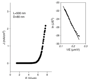
Fig. 3shows the FE characteristics for ZnO NW size of L = 500 nm and D = 80 nm. One can get Etoof 4.9 V/μm at current density of 1 μA/
cm2. As for the extraction of β, the Fowler–Norheim plot, ln(J/E2)
versus E− 1, is depicted in the inset. The linearity indicates the F–N relationship fits well the measured data. The F–N equation is as follows: J =Aβ 2 E2 ϕ exp −Bϕ 3= 2 βE !
where J is the current density, E the appliedfield, ϕ the work function of ZnO (5.37 eV),β the field enhancement factor, A=1.56×10− 10
Fig. 1. Schematic test system for FE measurements, in which the probe-tip distance d is much larger than the NWs length L.
Fig. 2. (a) The typical SEM cross-section images of the AAO template used as an aid to prepare the vertical ZnO NWs. (b) the TEM cross-section image of AAO full of ZnO.
Fig. 3. Field-emission current density versus electricfield for ZnO–NW with typical size of L = 500 nm and D = 80 nm. The inset shows the corresponding Fowler–Nordheim plots.
(AV− 2eV) and B = 6.83 × 10³(V eV− 3/2μm− 1)[13]. Thus, the value
ofβ can be calculated from the slope of the F–N plot, in which β is found to be about 1600 in this case. Thefield-emission ability and β value strongly depend upon the morphology of the ZnO NWs, including the geometry, structure tip size, and number of emitters on the substrate. Here we propose a simple way to examine roughly the Eto–β interdependence just from the F–N plot. The Etovalue turns
out approximately to be the reciprocal of the right end horizontal coordinate of the straight line in F–N plot. It means the slope has same inclination with Eto. With the slope relating to 1/β, a small Eto
corresponds to the higherβ value. This may be attained intuitively by sharping the tip size, i.e., reducing the turn-onfield via increasing the aspect ratio is expected to have a strongerfield enhancement. This indicates one can get optimal Etoandβ by L/D maximized. By glancing
at the two straight lines in the inset ofFig. 4, one will expect the less steep one being with lower Etoand enhancedβ.
3.3. Size effect
We verify this speculation by shrinking diameter down to 30 nm with L/D = 500 nm/80 nm for comparison. The corresponding J–E curve and F–N plot are shown inFig. 4for lines of white circle symbols. As expected, Etois down to 2 V/μm and β up to 4000. The second line
by black triangle symbol is for largest L of 1600 nm and smaller D of 30 nm to go forward in the case of maximized L/D. A profound enhancement of FE properties is obtained for L/D = 53 with Eto of
1.48 V/μm and β up to 6100. Separate length dependence is
investigated on emitters length in the range of 500–1600 nm and keep D = 80 nm unchanged.Fig. 5presents the results of measured Eto
and calculated β. The consistency of reduced Eto and larger β is
experimentally observed and confirmed by sharper tip size. One can probe this tendency with length via J–E in semi-log scale, as inFig. 6. Data inFig. 6are chosen fromFig. 5with L = 500, 1000, 1600 nm. The three segments in each curve represent different operation mode, so called respectively the off, active, saturation region with increasing
field[22,23]. The middle active operation width implies the linear
region in F–N plot. The fact that active E region width decreases with NW length agrees with thefinding of a smaller F–N plot slope with a larger 1/E right end.
So far, the observed size-dependent variations of Etoandβ are in
expectation. However, several factors may have impacts on the
feasibility of pursuing extreme L/D limit while keeping the effective improvement on FE effect. One is the process of hydrothermally grown ZnO within the nanochannels of the AAO templates. This poses the lower limit on D by considering the actualfilling efficiency and self-assembly quality. The limitation on D is also physically deter-mined by AAO interpore distance, which is controlled by the applied anodic voltage. Besides, the applied widening treatment to expand pore diameter simultaneously has the length shortening effect. The maximum length L available exists inevitably if simply extending the AAO growth time for formation of longer NWs. The phenomenon of uneven and large diameter of ZnO NW array should be considered, especially for those derived by chemical solution reaction compared with by vapor-phase approaches. It also needs dedicated techniques to synthesize high quality NWs at reasonable growth rate under low-temperature process. After all, large-scale, homogeneous, and dense NW arrays are essential for FE applications.
4. Conclusions
Field-emission measurement was conducted on nanowires based on ZnO 1-D nanostructure with high aspect ratio L/D. The size-dependent FE properties of lower Etoand higherβ are verified in this
study. We have prepared ZnO NWs based on two techniques. One is with the use of hydrothermal synthesis method to lower the fabrication temperature to 95 °C, and the other is with the aid of
Fig. 4. The emission current density and the corresponding F–N plots in inset, with size L–D as labeled.
Fig. 5. Dependence of the turn-onfield Etoand enhancement factorβ on NW length L,
withfixed diameter D=80 nm.
Fig. 6. Typical J–E curve in semi-log scale to highlight the active mode (middle segment by shadow) for FE. This operation region width decreases with NW length.
7285 C.-H. Lai et al. / Thin Solid Films 518 (2010) 7283–7286
AAO template to facilitate the manipulation of NW's length and diameter growth.
References
[1] H. Rensmo, K. Keis, H. Lindstroem, S. Soedergren, A. Solbrand, A. Hagfeldt, S.E. Lindquist, L.N. Wang, M. Muhammed, J. Phys. Chem. B 101 (1997) 2598. [2] Y. Lin, Z. Zhang, Z. Tang, F. Yuan, J. Li, Adv. Mater. Opt. Electron. 9 (1999) 205. [3] J.Y. Lee, Y.S. Choi, J.H. Kim, M.O. Park, S. Im, Thin Solid Films 403 (2002) 553. [4] M.H. Huang, S. Mao, H. Feick, H.Q. Yan, Y.Y. Wu, H. Kind, E. Weber, R. Russo, P.D.
Yang, Science 292 (2001) 1897.
[5] K.S. Weissenrieder, J. Mueller, Thin Solid Films 300 (1997) 30. [6] C.Y. Lee, T.Y. Tseng, S.Y. Li, P. Lin, J. Appl. Phys. 99 (2006) 24303. [7] R.C. Wang, C.P. Liu, J.L. Huang, S.J. Chen, Appl. Phys. Lett. 88 (2006) 023111. [8] S. Bhattacharyya, A. Rastogi, S.V. Bhat, K.S.R.K. Rao, A.V. Subramanyam, D. Kanjilal,
Solid State Commun. 105 (1998) 543.
[9] Z.W. Pan, Z.R. Dai, Z.L. Wang, Science 291 (2001) 1947.
[10] J.J. Wu, S.C. Liu, Adv. Mater. 14 (2002) 215.
[11] J.Y. Lao, J.Y. Huang, D.Z. Wang, Z.F. Ren, Nano Lett. 3 (2003) 235. [12] X.Y. Kong, Z.L. Wang, Appl. Phys. Lett. 84 (2004) 975.
[13] S.Y. Li, C.Y. Lee, P. Lin, T.Y. Tseng, J. Vac. Sci. Technol. B 24 (2006) 147. [14] S.H. Jo, J.Y. Lao, Z.F. Ren, R.A. Farrer, T. Baldacchini, J.T. Fourkas, Appl. Phys. Lett. 83
(2003) 4821.
[15] X.Y. Xue, L.M. Li, H.C. Yu, Y.J. Chen, Y.G. Wang, T.H. Wang, Appl. Phys. Lett. 89 (2006) 43118.
[16] S.Y. Li, C.Y. Lee, T.Y. Tseng, J. Cryst. Growth 247 (2003) 357.
[17] W.I. Park, D.H. Kim, S.W. Jung, G.C. Yi, Appl. Phys. Lett. 80 (2002) 4232. [18] B.D. Yao, Y.F. Chan, N. Wang, Appl. Phys. Lett. 81 (2002) 757.
[19] C.Y. Lee, S.Y. Li, P. Lin, T.Y. Tseng, IEEE Trans. Nanotechnol. 5 (2006) 216. [20] S.H. Jeong, H.Y. Hwang, Kun-Hong Lee, Y. Jeong, Appl. Phys. Lett. 78 (2001) 2052. [21] A.P. Li, F. Muller, A. Birner, K. Nielsch, U. Gosele, J. Appl. Phys. 84 (1998) 6023. [22] J.M. Bonard, C. Klinke, Phys. Rev. B 67 (2003) 115406.
[23] C.Y. Lee, T.Y. Tseng, S.Y. Li, P. Lin, Nanotechnology 17 (2006) 83. 7286 C.-H. Lai et al. / Thin Solid Films 518 (2010) 7283–7286