國立臺灣大學電機資訊學院電子工程學研究所 碩士論文
Graduate Institute of Electronics Engineering College of Electrical Engineering & Computer Science
National Taiwan University Master Thesis
電流切換開迴路殘值增益六位元導管式類比數位轉換器 A 6-bit Pipelined Analog-to-Digital Converter with Current-Switching Open-loop Residue Amplification
謝汾秋 Fen-Chiu Hsieh
指導教授:李泰成 博士 Advisor: Tai-Cheng Lee, Ph.D.
中華民國 97 年 7 月 July, 2008
摘要
由於積體電路製程進步,電晶體尺寸持續減小,單位面積的數位電路的運算 能力也不斷增加。但對於類比電路而言,較低的供給電壓與相對較大的臨界電 壓,反而造成了高速電路設計上的困難。類比數位轉換器連結了類比世界與數位 電路。由於在他的使用上延伸了純類比信號與類比數位混和信號的運作,類比數 位轉換器往往成為了資料運算應用上的瓶頸,限制了整個系統的速度與有效位元 數。
在這篇論文中,我們設計了一個以將管線式類比數位轉換器的 T/H 以及
MDAC 電路採用多路輸入架構,不用傳統的傳輸閘開關而使用電流操縱的方法 來做切換,使得速度不受開關電晶體大小的限制,開啟關閉不需要鋒對鋒時脈電 壓值,可節省時脈產生器的功率損耗。另外加上最近文獻提出的增益控制方法減
少增益誤差,來達成六位元低功率高速度的類比數位轉換器。設計使用 0.13 微
米製程與1.2 伏特的供給電壓,當類比數位轉換器運作在七億赫茲時脈速率時,
僅消耗24.1 毫瓦。
Abstract
By aggressive device scaling in modern integrated circuit technology, the computing ability of digital circuits increases significantly. But the low power supply and relative high threshold voltage of transistors exhibit design difficulties for analog circuit. Analog-to-digital converters provide the link between the analog and digital world. Due to their frequent use of analog and mixed analog-digital operations, A/D converters often appear as the bottleneck in data processing applications, limiting the overall speed or precision.
In this thesis, a 700-MHz 6-bit pipelined ADC with current-switching open-loop residue amplification and global-gain control is designed. Using a multiplexed-input architecture to implement T/H and MDAC circuits, transmission-gate switches are replaced by current-switching techniques. Without the need of digital calibration, a global-gain control technique is developed to eliminate the gain error. Fabricated in a 0.13-μm CMOS technology, the ADC consumes 24.1 mW from a 1.2-V power supply while the active area is only 0.052 mm2.
Table of Contents
Table of Contents I
List of Figures III
List of Tables VII
Chapter 1 Introduction 1
1.1 Motivation 1
1.2 Thesis Organization 3
Chapter 2 Fundamentals of Analog-to-Digital Converter 7
2.1 Introduction 7
2.2 ADC Performance Metrics 7
2.2.1 Signal-to-Noise Ratio (SNR) 8
2.2.2 Signal-to-(Noise + Distortion) Ratio (SNDR) 10 2.2.3 Resolution and Effective Number of Bits (ENOB) 10
2.2.4 Nonlinearity 11
2.3 Architecture of Analog-to-Digital Converters 13
2.3.1 Flash ADC 13
2.3.2 Two-Step Flash ADC 15
2.3.3 Pipelined ADC 16
2.3.4 Cyclic ADC 17
2.4 Summary 18
Chapter 3 The Design of Pipelined Analog-to-Digital
Converter 19
3.1 Introduction 19
3.2 Key Building Blocks of Pipelined ADC 20
3.3 Conventional Conversion Stage Design 25
3.3.1 Switched-Capacitor Technique 26
3.3.2 Switched-Capacitor MDAC 28
3.4 Low-Power High-Speed Conversion Stage Design 30
3.4.1 Differential Operation 31
3.4.2 Multiplexed-Input Architecture 39
3.4.3 Global-Gain Control 47
3.4.4 Dynamic Comparator 48
3.5 Nonideality Consideration 50
3.5.1 Open-loop Nonlinearity 50
3.5.2 Offset Error 54
3.6 Summary 56
Chapter 4 Circuit Implementation 57
4.1 Introduction 57
4.2 Track-and-Hold Circuit 58
4.3 MDAC Circuit 60
4.4 Global-Gain Control 64
4.5 Dynamic Comparator 66
4.6 Clock Generator and Divider 68
4.7 Digital Circuit and Output Buffer 71
4.8 The Simulation Results of Current-Switching Open-
Loop Pipelined ADC 73
4.9 Layout 78
4.10 Summary 79
Chapter 5 Test and Experimental Results 81
5.1 Introduction 81
5.2 Test Setup 81
5.3. Print Circuit Board Design 82
5.4 Experimental Results 85
5.5 Summary 91
Chapter 6 Conclusion 93
Bibliography 95
List of Figures
Chapter 1
Figure 1.1 Performances of recent ADCs in different architectures. 2
Chapter 2
Figure 2.1 The probability density function of the quantization error. 9 Figure 2.2 Transfer function including error sources.
(a) Offset error, (b) missing code. 12
Figure 2.3 Transfer characteristic of ADC showing DNL and INL. 13 Figure 2.4 The block diagram of a flash ADC. 14
Figure 2.5 Two-step ADC architecture. 15
Figure 2.6 The block diagram of a pipelined ADC. 17
Figure 2.7 The cyclic ADC topology. 18
Chapter 3
Figure 3.1 The block diagram of general pipelined ADC. 20
Figure 3.2 Pipelined ADC timing. 21
Figure 3.3 1.5-bit conversion stage transfer curve. 22 Figure 3.4 One-bit conversion stage transfer curve. 23
Figure 3.5 1.5-bit code combination. 24
Figure 3.6 1.5-bit conversion stage architecture. 26
Figure 3.7 MOS sample-and-hold circuit. 27
Figure 3.8 Switched-capacitor MDAC. 29
Figure 3.9 Closed-loop and open-loop residue amplifier. 31 Figure 3.10 (a) Simgle-ended and (b) differential signals. 32
Figure 3.11 Basic differential pair. 33
Figure 3.12 Variation of drain currents and overall transconductance
of a differential pair versus input differential voltage. 36 Figure 3.13 Common-source stage with resistive degeneration. 38
Figure 3.14 Source degeneration applied to a differential pair. 39 Figure 3.15 Multiplexed-input architecture. (a) Basic (single-ended)
circuit; (b) Equivalent circuit in the hold mode. 40 Figure 3.16 Schematic of multiplexed-input architecture. 42 Figure 3.17 MDAC of multiplexed-input architecture. 44 Figure 3.18 Schematic of MDAC with multiplexed-input architecture. 45
Figure 3.19 Open-loop residue amplifier. 46
Figure 3.20 Global-gain control. 48
Figure 3.21 Dynamic comparator. 49
Figure 3.22 Open-loop circuit model. 50
Figure 3.23 Basic differential pair. 51
Figure 3.24 Simple sampling circuit. 54
Chapter 4
Figure 4.1 The architecture of pipelined ADC. 58
Figure 4.2 Schematic of T/H. 59
Figure 4.3 Output voltage of T/H circuit. 60
Figure 4.4 MDAC of multiplexed-input architecture. 60 Figure 4.5 (a) Schematic of MDAC with multiplexed-input architecture;
(b) Open-loop residue amplifier. 62
Figure 4.6 The simulation results of MDAC circuit. 64 Figure 4.7 (a) Global-gain control; (b) Error amplifier. 65
Figure 4.8 Dynamic comparator. 67
Figure 4.9 Schematic of clock buffer. 68
Figure 4.10 Simulation results of clock generator. 68 Figure 4.11 (a) Track-and-hold circuit. (b) MDAC circuit. 69
Figure 4.12 Block diagram of divider. 70
Figure 4.13 Output synchronization and retiming. 71 Figure 4.14 (a) The simulated effects about the pad, bonding wire and
the probe. (b) The output buffer. 72
Figure 4.15 The simulation results of INL and DNL. 73 Figure 4.16 The FFT spectrum with 357-MHz input frequency and 714-
MSPS. 74 Figure 4.17 The FFT spectrum with 714-MHz input frequency and 714-
MSPS. 75 Figure 4.18 The SNDR versus conversion period. 76
Figure 4.20 Layout of 0.13-μm prototype. 78
Chapter 5
Figure 5.1 Test setup. 82
Figure 5.2 The photograph of PCB. 83
Figure 5.3 (a) The pin configurations of the ADC.
(b) The description of pin configurations. 83 Figure 5.4 Die photomicrograph of the prototype chip. 85 Figure 5.5 Measured results of (a) output clock and (b) plot chart. 86
Figure 5.6 Measured INL and DNL. 87
Figure 5.7 (a) FFT of 256-kHz input at 700 Msample/s.
(b) FFT of 349.9-MHz input at 700 Msample/s. 88 Figure 5.8 (a) SNDR and SFDR versus conversion rate with 80-MHz input.
(b) SNDR and SFDR versus input frequency at 700 Msample/s. 89 Figure 5.9 The Monte Carlo simulation of track-and-hold circuit. 90
List of Tables
Chapter 1
Chapter 2
Chapter 3
Chapter 4
Table 4.1. Summary of transistor sizes and component value of T/H circuit. 59 Table 4.2. Summary of transistor sizes and component value of the MDAC
Circuit. 63 Table 4.3. Summary of transistor sizes and component value of open-loop
residue amplifier. 63 Table 4.4. Summary of transistor sizes of error amplifier. 66 Table 4.5. Summary of transistor sizes of the comparator. 67 Table 4.6. The post-layout simulation results of extreme cases. 77
Table 4.7. Summary of the taped-out ADC. 79
Chapter 5
Table 5.1. Summary of measured results of the pipelined ADC. 91
Chapter 1
Introduction
1.1 Motivation
Analog-to-digital converters provide the link between the analog world and the digital system. Due to their extensive use of analog and mixed analog-digital operations, A/D converters often appear as the bottleneck in data processing applications, limiting the overall speed or precision [1].
In recent years, the demand for high-speed A/D converters has grown rapidly in automated test equipment, oscilloscopes and digital read channel systems. However, low power consumption and small area are more important than higher conversion rate and input bandwidth for these purposes [2, 3]. The pipelined architecture offers power and/or speed advantages over flash or multi-step approaches due to concurrent processing of analog signals [4].
Figure 1.1. Performances of recent ADCs in different architectures [5].
The performance of recent ADCs in different architecture is illustrated in Fig. 1.1. It can be observed that pipelined ADC usually works on hundreds of mega hertz. Conventional pipelined ADCs use electronic feedback to achieve highly linear and drift insensitive transfer characteristics in their conversion stages. Especially, the converter front-end amplifiers with large open-loop gain are needed to achieve the desired accuracy. Due to stringent design trade-offs between low noise and high bandwidth requirements, precision amplifiers dominate the power dissipation in most high speed designs [6, 7].
As the trend to deep-submicron technologies, the device scales down aggressively in recent years, leading to the improvement of computing power of digital circuits. However, the scaling down of supply voltage and threshold
voltage imposes the critical limitation of analog circuit design. For example, telescopic amplifier is hard to implement in deep-submicron technology because of the limited headroom of power supply. Thus, the compatibility with deep-submicron technologies has emerged as important metrics in state-of-the-art ADC design.
In this work, the multiplexed-input architecture [1] is employed to implement track and hold and MDAC circuit, operating in high speed and low power consumption for a 1.5-b/stage pipelined A/D converter. Instead of conventional switched-capacitor circuits, current-steering method is used to perform circuit switching. It allows low-swing operation and needs no rail-to-rail clock, so the power consumption of the clock generator can be low. Furthermore, the proposed global-gain control method [8] is used to eliminate the parasitic voltage division of gain loss in open-loop amplification.
1.2 Thesis Organization
This thesis consists of six chapters. A brief introduction of this thesis is described in Chapter one. Chapter two starts with the performance metrics used in ADC
design. And then the basic analog-to-digital converter architectures are presented, including flash, two-step, pipelined, and cyclic architectures.
Chapter three focus on the design concept of the pipelined ADC. The constraints of conventional MDAC circuit is considered and analyzed. Based on multiplexed-input architecture, current-switching open-loop amplifiers operating in high speed and low power consumption are proposed. Without the need of digital calibration, global-gain control method is concluded to improve the gain error.
Chapter four shows the implementations of the 700-MHz 6-bit pipelined ADC with current-switching open-loop amplifiers. The circuits of building blocks are designed and simulated. The whole system simulation and layout floorplan are depicted in the end of the chapter.
Chapter five presents the testing strategy of the ADC systems. The testing environment including the measurement instruments and print-circuit-board design are introduced. Then the experimental results of the prototype are shown.
In the end of this thesis, conclusions of the pipelined ADC prototype design are summarized in Chapter six.
Chapter 2
Fundamentals of Analog-to-Digital Converter
2.1 Introduction
This chapter reviews some of the fundamental issues in the design of a pipelined analog-to-digital converter. In order to characterize the ADCs thoroughly, a number of performance metrics are defined. Following a definition of performance metrics, we describe a number of A/D converter architectures commonly employed in high performance systems.
2.2 ADC Performance Metrics
To fully specify the performance of ADCs requires a large number of parameters, some of which are defined differently by different manufactures. In this section, the definitions of a number of important metrics used are described.
2.2.1 Signal-to-Noise Ratio (SNR)
Signal-to-noise ratio (SNR) is the ratio of the signal power to the total noise power at the output, usually measured for a sinusoidal input. The approximation or “rounding” effect in A/D converters is called “quantization,” and the difference between the original input and the digitized output is called the
“quantization error,” even occurred in ideal A/D converters. To deal with the general input case, a stochastic approach is typically used. In a stochastic approach, we assume that the input signal is varying rapidly such that the quantization error signal, VQ, is a random variable uniformly distributed between
LSB 2
±V . The probability density function for such an error signal, fQ
( )
x , will be a constant value, as shown in Fig. 2.1.Hence, the R.M.S. value of the quantization error is given by
( )
121 2 12
2 2 2
2 1
, V LSB
LSB V e
RMS Q
dx V V x
dx x f x
V LSB
LSB
⎥ =
⎦
⎢ ⎤
⎣
⎡ ⎜⎝⎛ ⎟⎠⎞
⎥⎦ =
⎢⎣ ⎤
=⎡∫ ∫−
∞
∞
− . (2.1)
In general, the R.M.S. quantization noise power equals VLSB 12 when the quantization noise signal is uniformly distributed over the interval ±VLSB 2.
2
−Δ
2 Δ
Δ 1
Figure 2.1. The probability density function of the quantization error.
Thus, given an input signal waveform, a formula can be derived giving the best possible signal-to-noise ratio (SNR) for a given number of bits in an ideal A/D converter. Assuming V is a sinusoidal waveform between in
VREF
± , thus the ac power of the sinusoidal wave is VREF 2and for an N-bit ideal ADC, the VLSB equals to 2VREF 2N , which results in
SNR ⎟⎟
⎠
⎞
⎜⎜
⎝
= ⎛
RMS Q
RMS in
V V
,
log ,
20 (2.2)
( ) ( )
⎟⎟⎠⎞⎜⎜⎝
= ⎛
12 2 log 2
20
LSB REF
V
V (2.3)
⎟⎟⎠
⎞
⎜⎜⎝
= ⎛ 2N
2 log 3
20 . (2.4)
SNR =6.02N+1.76 dB, (2.5)
Note that (2.5) gives the best possible SNR for an N-bit A/D converter.
However, the idealized SNR decreases from this best possible value for reduced input signal levels [11].
2.2.2 Signal-to-(Noise + Distortion) Ratio (SNDR)
The signal-to-(noise + distortion) ratio (SNDR) is the ratio of the signal power to the total noise and harmonic power at the output, when the input is a sinusoid.
Only considering the quantization noise for an N-bit ADC, the best possible SNR can reach (2.5). But in real world, more other effect must be concerned, such as harmonic distortion and noise. When a single-tone sinusoidal signal apply to an N-bit ADC, the output codes generally contain a signal component at the input frequency. Due to distortions, the output also contains harmonic components in the spectrum. Furthermore, the extra noise power added to the circuit will contribute to all frequencies. If the power of harmonic distortion and noise is over the noise floor, even for N-bit resolution codes, the measured SNDR will be less than SNR.
2.2.3 Resolution and Effective Number of Bits (ENOB)
The resolution of a converter is defined to be the number of distinct analog levels corresponding to the different digital words. Thus, an N-bit resolution implies that the converter can resolve 2N distinct analog levels. Resolution is not
necessarily an indication of the accuracy of the converter, but instead it usually refers to the number of digital input or output bits [9].
The effective number of bits (ENOB) can be treated as the reverse computation of the (2.5). ENOB defines the “effective” number of bits based on the measured results, SNDR. It is defined by the following equation:
02 . 6
76 .
−1
=SNDRp
ENOB , (2.6)
where SNDRp is the peak SNDR of the converter expressed in decibels.
2.2.4 Nonlinearity
Another estimation method is to plot the input/output characteristic of the A/D converter. The transfer characteristic for an ideal ADC progresses from low to high in a series of uniform steps. As the resolution increases, the input/output characteristic of ADC approximates a straight line. In practical ADC, the steps are not perfectly uniform due to nonidealities, such as offset error, gain error, and linearity error. Figure 2.2 shows the deviation of transfer characteristics resulted
from nonidealities.
(a) (b)
Figure 2.2. Transfer function including error sources. (a) Offset error, (b) missing code.
Two types of nonlinearity measurement metrics are used to characterize this deviation. Differential nonlinearity (DNL) is the maximum deviation in the difference between two consecutive code transition points on the input axis from the ideal value of 1 LSB. Integral nonlinearity (INL) is the maximum deviation of the input/output characteristic from a straight line passed through its end points. Figure 2.3 illustrates the DNL and INL, which can be expressed as:
( )
iDNL
( ) ( )
11
1− −
= +
LSB i UB i
UB ; (2.7)
( )
iINL
( ) ( )
LSB i UB i
UB ideal
1
= − , (2.7)
where UB(i) is the transition level of i-th code [1, 10].
Figure 2.3. Transfer characteristic of ADC showing DNL and INL.
2.3 Architectures of Analog-to-Digital Converters
The architectures of A/D converters can be broadly classified as one-step or multi-step, with flash in the first category and two-step, cyclic, and pipelined configurations in the second. Each of architecture has advantages and disadvantages, contributing for different applications [1]. In the following, the basic architectures of A/D converter are introduced.
2.3.1 Flash ADC
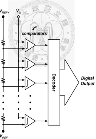
Flash-type architectures are typically the simplest and fastest structures that can be used to implement these very high-speed A/D converters. Figure 2.4 is a block
diagram of an n-bit flash ADC, consisting of an array of 2N comparators, a resistor ladder comprising 2N equal segments, and a decoder. The ladder subdivides the main reference into 2N equally spaced voltages, and the comparators compare the input signal with these voltages. Consequently, the comparator outputs constitute a thermometer code, which is converted to binary by the decoder. Due to the parallel operation of comparators, the flash ADC is capable of high conversion speed [1, 11].
Figure 2.4. The block diagram of flash ADC.
The demand of comparators growing exponentially with resolution is the main drawback of flash ADC, leading to the large input capacitance and great gate counts. Thus the flash ADCs require excessively large power and area for resolution above 8 bits. Furthermore, the large number of comparators may give rise to the problem of capacitor feed through and kickback noise between the analog input and the resistor ladder.
2.3.2 Two-Step Flash ADC
The exponential growth of power, area, and input capacitance of flash ADCs as a function of resolution makes them impractical for high-resolution design.
Two-step architectures trading speed for power, area and input capacitance provide another solution.
∑
Φ2
Φ1
Figure 2.5. Two-step ADC architecture.
A two-step flash ADC consists of two flash sub-ADCs as shown in Fig. 2.5.
During the first step, the coarse ADC estimate the analog input and determine the most significant bits (MSB) of the output code. Then a DAC converts the digital output to a reference analog voltage, subtracted by the input signal. The analog residue is estimated by the fine ADC to generate the left bits of the output code.
Though the conversion time of the two-step ADC is longer than the flash ADC,
only 2⋅2N2 comparators of the two-step ADC are required, relaxes the hardware complexity significantly [12,13].
2.3.3 Pipelined ADC
Unlike the parallel conversion of flash-type architecture, the two-stage architecture described in previous section can be generalized to multiple stages.
Depicted in Fig. 2.6, the pipelined ADC adopts the serial conversion and incorporates the pipeline concept used widely in digital signal processor. The analog signal is sampled and held at the front-end, and then processed stage by stage. With S/H circuit added to each stage, the constraints of stage design are relaxed but the digital output latency is increased because the signal must transfer through all of the stages before the complete output word is generated.
One significant implication of this is that the sub-ADC in the last stages of the pipeline need not be accurate to the full ADC resolution as they are required in other subranging ADCs. Furthermore, with many developed digital calibration, the nonidealities of comparator and amplifier can be easily corrected.
∑
Figure 2.6. The block diagram of pipelined ADC.
2.3.4 Cyclic ADC
The most attractive advantage of the cyclic ADC is the very little hardware and low power consumption. A cyclic ADC can be realized as a single pipelined stage with the output fed back to the input, and such a topology is illustrated in Figure. 2.7. The latency of a cyclic ADC is the same as the pipelined architecture;
however, the throughput is much more than for a pipelined ADC because the new sample must be taken after the output codes are generated completely [1].
∑
Figure 2.7. The cyclic ADC topology.
2.4 Summary
This chapter has described the basic measurement metrics used to characterize the A/D converter and reviewed some prominent ADC architectures. It can be observed that the pipelined architecture has the potential to achieve high-speed- high-resolution design because of simple conversion stage design and linear hardware complexity growth.
Chapter 3
The Design of Pipelined Analog-to-Digital Converter
3.1 Introduction
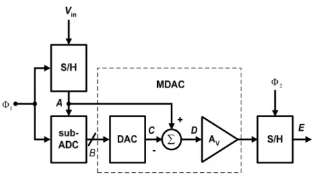
In the previous chapter, we have described the basic architecture of pipelined ADC. In the following, the 1.5-bit/stage design is described in detail. A pipelined ADC is composed of a track-and-hold circuit, followed by four MDACs, and backend 2-bit flash ADC. For realizing a pipelined ADC with low power and high-speed design, current-switching open-loop residue amplifiers are presented.
Instead of conventional switched-capacitor circuits, multiplexed-input architecture [1] with the method of current-switching is used. It allows low-swing operation and needs no rail-to-rail clock. The power of the clock generator can be low. The residue gain is controlled by the proposed method, global-gain control [8].
3.2 Key Building Blocks of Pipelined ADC
The block diagram of general pipelined ADC is shown in Fig. 3.1. A pipelined ADC is composed of replica stages, each including a sample-and-hold circuit (S/H), an ADC, a DAC, a subtractor and an amplifier. Within each stage, a typical conversion proceeds as follows. The pipelined stage samples and then holds analog input signal, resolves digital codes from the held input, converts the N-bit codes to analog, subtracts the result from the held input, and amplifies the residue by a power of 2N. Next, the following stage in the pipeline samples the residue and performs the same sequence of operations while the first stage begins processing the next sample.
∑
Figure 3.1. The block diagram of general pipelined ADC.
Φ1
Φ2
Figure 3.2. Pipelined ADC timing.
The beginning S/H relaxes the timing requirements of the backward operation during its sampling phase by holding the instantaneous value of the analog input. Once the S/H has acquired the data, begins the same operation on the next stage. Thus, at any given time, all the stages are processing different samples concurrently, and hence the throughput rate depends only on the speed of each stage and the acquisition time of the next S/H. Consequently, the conversion rate usually only depends on the speed of stage design.
The basic pipelined ADC timing is shown in Fig. 3.2. Two-phase, non-overlapping clocks Φ1 and Φ2 are used. The analog input to the
pipelined ADC is presented to the first stage while Φ1 is high. At the end of phase Φ1, the analog input is held by the S/H. At the same time, the sub-ADC monitoring the input signal is strobed and the digital output codes are determined.
When Φ2 goes high, the stage one switches to amplify mode, where the sub-DAC, subtractor and amplifier determine the analog residue according the held signal and digital estimate, and its output is presented to the input of stage two. At the end of phase Φ2, the analog input presented to the stage two is held and quantized. This process continues until the ADC input data in question reaches the end of the pipeline. New ADC input data is samples at the end of each phase Φ1. Thus the throughput of the ADC is the period of the clock.
Figure 3.3. 1.5-bit conversion stage transfer curve.
The stage transfer curve of 1.5-bit conversion is illustrated in Fig. 3.3. The sub-ADC resolves 2-bit digital code, and it means that the full-scale input range
is taken into three sub-ranges, where the transition points are ±VREF /4. According to the location of the sub-ranges, the input signal subtracts the reference value, converted by sub-DAC, and yields the analog residue. The analog residue is then restored to the original full-scale input range of conversion stage by the amplifier. Thus, the analog output can be described as
DAC IN
OUT V DV
V =2 − ⋅ , (3.1)
Figure 3.4. One-bit conversion stage transfer curve.
where D can be +1, 0 or -1 and correspond to digital output codes, 00 , 01, 10 individually. If we avoid code 01 region, D will be equal to +1 or -1 and the digital output will be 0 or 1. A traditional 1-bit per stage ADC is recovered shown as Fig. 3.4. In 1-bit per stage pipelined ADC, the processed signal has the probability to be larger than +VREFor less than −VREF caused by comparator
offset and capacitor mismatch. This out-of-range output signal will saturate the latter stage and degrade the ADC performance. In 1.5-bit per stage pipelined ADC, the code 01 region can be taken as a buffer region. Unless the offset voltage of comparators is larger than VREF /4, the out-of-range problem will not occur. Take a 4-bit system as an example, the code combination is shown as Fig.
3.5.
Figure 3.5. 1.5-bit code combination.
The existence of residue amplification stage has two folds. First, the requirement of reference voltages is reduced. For example, if the specification of ADC is N bits, flash architecture requires 2N reference voltages. However, for k-bit/stage pipelined ADC, k is less than N, only 2k reference voltages are needed to guarantee full swing input and output. Second, the maximum allowable gain error and nonlinearity of the sample-and-hold circuit and residue amplifier in each stage is commensurate with the number of bits resolved afterward. Thus,
following stages.
3.3 Conventional Conversion Stage Design
Shown in Fig. 3.6, when Φ1 goes low, the input signal is held and the digital code is determined. Before Φ1 goes low, we know that the signal on node E should be settled down. The critical path is from node B to node E, the signal line through the DAC, the subtractor, the amplifier and the S/H of the next stage.
Typically, the function of the sub-DAC, the subtraction and the amplification of the residue could be combined into one single circuit called the multiplying DAC (MDAC). While the concurrent operation of pipelined converters leads itself to the high-speed design, their extensive linear processing of the analog signal relies heavily on the MDAC circuits, relatively slow building blocks in analog design.
∑ Φ1
Φ2
Figure 3.6. 1.5-bit conversion stage architecture.
3.3.1 Switched-Capacitor Technique
Switched-capacitor (SC) technique is pervasive in highly integrated, mixed- signal applications. It is one of the most important methods to build analog circuits due to its sample-and-hold (S/H) functionality and good linearity. The S/H circuit is the most basic and ubiquitous switched-capacitor building block.
Before a signal is processed by a discrete time system, such as an ADC, it must be sampled and stored. This often greatly relaxes the bandwidth requirements of the following circuit that now can work with a “DC” voltage. Because the S/H is often the first block in the signal process systems, the accuracy and speed of entire applications cannot exceed that of the S/H [12].
Figure 3.7. MOS sample-and-hold circuit.
In the CMOS technology, the simplest S/H consists of a MOS switch and a capacitor as shown in Fig. 3.7. When VCTRL is high, the NMOS transistor acts like a linear resistor, allowing the output V to track the input signalout V . When in
VCTRL goes low, the transistor cuts off and isolates the input from the output, and the signal is held on the capacitor at V . The NMOS was treated as a resistor. out In reality, the MOS resistor deeply depends on the voltage level of the input signal. In the case of the NMOS, if the turn-on voltage of the gate is VDD and the source and drain voltage is much smaller than VDD–VTH, then the transistor must operates in triode region and the following current is
NMOS
ID, ( ) ⎥
⎦
⎢ ⎤
⎣
⎡ − ⋅ −
⎟⎠
⎜ ⎞
⎝
= ⎛
2
2
, DS
DS N TH GS N OX N
V V V L V
C W
μ (3.2)
( GS IN TH N) DS
N OX
N V V V V
L
C W ⎟ − − ⋅
⎠
⎜ ⎞
⎝
≅μ ⎛ , . (3.3)
Then, the turn-on resistance of the NMOS is given by
( GS IN TH N)
N OX NMOS N
D DS NMOS on
V V L V
C W I
R V
, , ,
1
−
⎟ −
⎠
⎜ ⎞
⎝
= ⎛
=
μ
. (3.4)
Large W/L ratio must be used to get low Ron , and then the sampling speed will be faster. But when the size is larger, the parasitic capacitor is bigger, so the speed is limited. To enlarge turn-on voltage is needed to diminish Ron , so rail-to-rail clock voltage is necessary. It costs lots of power consumption in clock generator buffers.
3.3.2 Switched-Capacitor MDAC
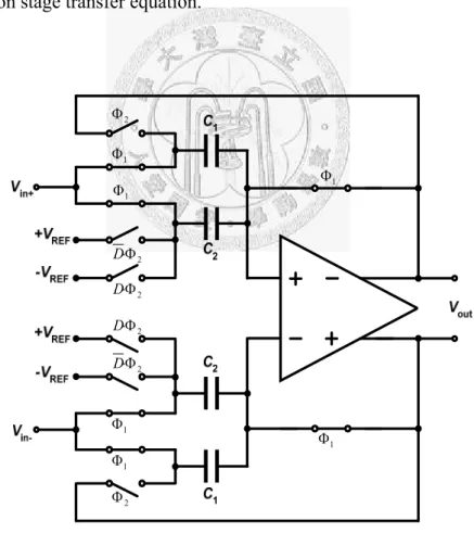
In order to implement the S/H function that is crucial for the concurrent operation and to achieve high linearity, the SC circuit is feasible implementation for the MDAC. The conventional structure of a SC MDAC is shown in Fig. 3.8.
The circuit corresponds to one stage of a pipelined A/D and consists of nominally identical capacitors C1 and C2 and an op amp A. A typical conversion cycle proceeds as follows. In phase Φ1, the analog input is sampled
on C1 and C2. Next, the dc loop around A opens, C1 is placed around A, and
C2 is switched to +VREF or −VREF , determined by the digital estimate of the sub-ADC. The output voltage then equals
REF in
out V DV
C C
V C + − ⋅
=
1 2
1 . (3.5)
If C1 is equal to C2 , this equation corresponds to (3.1), the 1.5-bit conversion stage transfer equation.
Φ1
Φ1
Φ1
Φ1
Φ2
Φ2
Φ1
Φ1
Φ2
⋅ D Φ2
D⋅
Φ2
D⋅ Φ2
D⋅
Figure 3.8. Switched-capacitor MDAC.
However, the drawback of this circuit is limited by speed. This is due to the fact that turn-on time is needed for the op amp to recover from its switched-off state to the active stage [14, 15]. To attain high-speed operation in the conversion stage, the op amps utilized in each stage should employ large devices biased at high currents, thereby dissipating high power consumption.
3.4 Low-Power High-Speed Conversion Stage Design
Recently, the benefits of using open-loop structures in high-speed pipelined ADCs have been recognized and demonstrated. The 8-bit ADCs reported in [16]
and [17] use open-loop current-mode residue amplification to achieve excellent power efficiency at high conversion speeds. Another 12-bit ADC reported in [6, 7] achieves 60% residue amplifier power savings over a conventional implementation by using the voltage-mode open-loop amplifier. In this section, the comparison of open-loop and closed-loop amplifiers and the basic concept of open-loop residue amplification circuit are introduced firstly. Current-switching open-loop amplifiers with global-gain control method developed in the T/H and MDAC circuits are described. The dynamic comparator is also described because of its ultra low-power characteristic.
Figure 3.9. Closed-loop and open-loop residue amplifier.
Considering the Fig. 3.9, closed-loop and high-gain operational amplifiers are traditionally used in residue amplification stage. The ratio of capacitors decides the closed-loop amplifier gain precisely with high-gain operational amplifier techniques such as telescopic, folded-cascode, two-stage and gain-boosting. As discussed before, the high-gain and high-speed operational amplifiers both suffer from the same meaning with power inefficiency. So it is replaced by open-loop amplifier. It costs less power consumption but more nonlinearity effects.
3.4.1 Differential Operation
A single-ended signal is defined as one that is measured with respect to a fixed potential, usually the ground. A differential signal is defined as one that is
measured between two nodes that have equal and opposite signal excursions around a fixed potential. In the strict sense, the two nodes must also exhibit equal impedances to that potential. Figure 3.10 illustrates the two types of signals conceptually. The “center” potential in differential signaling is called the
“common-mode” (CM) level.
Figure 3.10. (a) Single-ended and (b) differential signals.
An important advantage of differential operation over single-ended signaling is higher immunity to “environmental” noise. Another useful property of differential signaling is the increase in maximum achievable voltage swings.
Other advantages of differential circuits over single-ended counterparts include simpler biasing and higher linearity [17].
In Fig. 3.11, the basic common source differential pair is shown. Employing the common current source I and assuming the circuit is symmetric, SS M1
and Vin2 −VGS2,
2 1 2
1 in GS GS
in V V V
V − = − , (3.6)
Figure 3.11. Basic differential pair.
For a square-law device,
( )
L C W V I
V
OX n TH D
GS μ
2 1
2 =
− , (3.7)
and therefore,
TH OX
n D
GS V
L C W
V = I +
μ
2 . (3.8)
It follows from (3.6) and (3.8) that
L C W
I
L C W V I
V
OX n
D
OX n
D in
in μ μ
2 1
2 1
2
2 +
=
− . (3.9)
Squaring the two sides of (3.9) and recognizing that ID1 +ID2 =ISS,
( ) (
1 2)
2 2
1 2 2
D D SS
OX n in
in I I I
L C W V
V − = −
μ
. (3.10)
That is,
(
1 2)
2 2 1 22 1
D D SS
in in OX
n V V I I I
L
C W − − =−
μ . (3.11)
Squaring the two sides again and noting that 4ID1ID2 =
(
ID1 −ID2)
2 −(
ID1 −ID2)
2 =ISS2 −(
ID1 −ID2)
2, the folloing equation can be arrived:(
1 2)
2 2(
1 2)
4(
1 2)
24 1
in in OX n SS in
in OX
n D
D V V
L C W I V
L V C W I
I ⎟ − + −
⎠
⎜ ⎞
⎝
− ⎛
=
− μ μ . (3.12)
Thus,
(
1 2) (
1 2)
22 1
4 2
1
in in OX
n SS in
in OX
n D
D V V
L C W V I
L V C W I
I − = − + − −
μ
μ . (3.13)
As expected, ID1−ID2 is an odd function of Vin1−Vin2, falling to zero for
2
1 in
in V
V = . Denoting ID1−ID2 and Vin1−Vin2 by ΔIDand ΔVin, respectively, the reader can show that
2 2
4 4 2 2
1
in OX
n SS
in OX
n SS
OX n in
D
L V W C
I L V W C
I
L C W V
I
Δ
− Δ
− Δ =
∂ Δ
∂
μ
μ μ , (3.14)
for 0ΔVin = , Gm = μnCOX
(
W L)
ISS .Moreover, since Vout1−Vout2 =RDΔI =in m
DG V
R Δ , we can write the small-signal differential voltage gain of the circuit in the equilibrium condition as
D SS OX n
v I R
L C W
A = μ . (3.15)
Because each transistor carries approximately ISS 2 in the vicinity of equilibrium, the small-signal differential gain can be simplified to
D m
v g R
A = , (3.16)
where g denotes the transconductance of m M1 and M2. Equation (3.14) also suggests that G falls to zero for m ΔVin = 2ISS
(
μnCOXW L)
. It is because that (3.14) is derived with the assumption that both M1 and M2 are on. In reality, as ΔVin exceeds a limit, one transistor carries the entire I , turning off SS the other. Denoting this value by ΔVin1 , we have ID1 =ISS andTH GS
Vin =Δ −Δ
Δ 1 1 because M2 is nearly off. It follows that
L C W V I
OX n in SS
μ 2
1=
Δ . (3.17)
For ΔVin >ΔVin1, M2 is off and (3.17) does not hold. As mentioned above,
G falls to zero for m ΔVin =ΔVin1. Figure 3.12 plots the characteristics.
Figure 3.12. Variation of drain currents and overall transconductance of a differential pair versus
input voltage.
The value of ΔVin1 given by (3.17) in essence represents the maximum differential input that the circuit can “handle.” It is possible to relate ΔVin1 to the overdrive of M1 and M2 in equilibrium. For a zero differential input,
2 2
1 D SS
D I I
I = = , and hence
( )
L C W V I
V
OX n
SS TH
GS − 1,2 = μ . (3.18)
Thus, the equilibrium overdrive is equal to ΔVin1 2. The point is that increasing ΔVin1 to make the circuit more linear inevitably increase the overdrive voltage of M1 and M2. For a given I , this is accomplished only SS by reducing W L and hence the transconductance of the transistors.
Source Degeneration The simplest linearization method uses source degeneration by means of a linear resistor. Shown in Fig. 3.13, for a common-source stage, degeneration reduces the signal swing applied between the gate and the source of the transistor, thereby making the input/output characteristic more linear. From another point of view, neglecting body effect, the overall transconductance of the stage is written as
S m m
m g R
G g
= +
1 , (3.19)
indicating that large gmRS makes G equal to m 1 RS , an input-independent value.
Figure 3.13. Common-source stage with resistive degeneration.
Note that the amount of linearization depends on gmRS rather on R S alone. With a relatively constant G , the voltage gain, m GmRD, is also relatively independent of the input and the amplifier is linearized [18].
(a) (b) Figure 3.14. Source degeneration applied to a differential pair.
A differential pair can be degenerated as shown in Figs. 3.14(a) and 3.14(b).
In Fig. 3.14(a), ISS flows through the degeneration resistors, thereby consuming a voltage headroom of ISSRS 2, an important issue if a high level of degeneration is required. The circuit of Fig. 3.14(b), on the other hand, does not involve this issue but it suffers from a slightly higher noise (and offset voltage) because the two tail current sources introduce some differential error.
3.4.2 Multiplexed-Input Architecture
Fig. 3.15(a) shows the single-ended version of a multiplexed-input SHA originally proposed by Ryan [19] and later modified by Petschacher et al. [20]. It
consists of transconductance amplifiers Gm1, Gm2 and transresistance amplifier R.
Nominally, Gm1R = Gm2R = 1. Amplifiers Gm1 and Gm2 are controlled (i.e.,
multiplexed) by CK andCK. During sampling, Gm1 is enabled, Gm2 is disabled, and Gm1 and R operate as a unity-gain amplifier, allowing Vout to track Vin. Note that the acquisition time constant is given primarily by the output resistance of R and the value of CH. In the transition to the hold mode, Gm1 is disabled, Gm2 is enabled, and Gm2 and R are configured as a unity-gain amplifier, thereby retaining the sampled value of Vin across CH.
Gm1 R
Gm2
CH
Vin Vout
CK CK
(a)
Rout A
CH VX
Vout
(b)
Figure 3.15. Multiplexed-input architecture. (a) Basic (single-ended) circuit; (b)
In order to illustrate the hold-mode operation, a simplified version of the circuit is shown in Fig. 3.15(b), where A = Gm2R (≈ 1) and Rout represents the open-loop output resistance of the amplifier. Assuming CH is charged to a voltage Vo at the end of the acquisition mode and neglecting the input bias current of A, the following equation can be arrived:
dt C dV R
V
V out
H out
X
out − =−
, (3.20)
and
out
X AV
V = , (3.21)
Thus,
τ V t
Vout = oexp− , (3.22)
where τ =RoutCH/
(
1−A)
and the origin of time is the beginning of the hold mode. Equation (3.22) shows that if A = 1, then τ =∞; i.e., the droop rate is zero and Vout will remain at Vo definitely. If A= 1−ε, then Vout decays with a time constant equals to RoutCH /ε; i.e.; the droop time constant is 1/ε times the acquisition time constant. While achieving high speed, the architecture of Fig.3.15 entails several challenges if employed for high-resolution applications. The acquisition time constant and the droop rate trade off according to the deviation of A from unity.
M1 M2 Vin
ISS R
VDD R
M3 M4
Vout
Rs1 Rs1 Rs2 Rs2
CK CK
CH
CK M7CK M8
M5 M6
Figure 3.16. Schematic of multiplexed-input architecture.
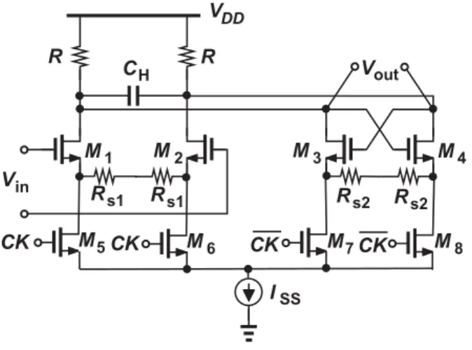
The circuit detail is shown in Fig. 3.16. To allow proper operation, the equivalent gain of track and hold mode, corresponding to gm1,2R/(1+gm1,2Rs1) and )gm3,4R/(1+gm3,4Rs2 , must be equal to unity. During sampling, CK = high, M1,2 turn on and M3,4 turn off, so Vout tracks the value of Vin. In the transition to the hold mode, CK = low, M3,4 turn on and M1,2 turn off, so Vout holds the value stored in CH, which equals to Vin. Just as described before, transmission-gate switches need rail-to-rail clock swing and large W/L ratios, the speed will be limited by turn-on resistance. And the rise/fall time of full swing non-overlap
clock is about 0.2 ns for a 0.13-μm CMOS technology, the ADC barely operates over 500 MHz. Additionally, a frequency-dependent nonlinearity error in MOS sampling circuits arises from the variation of the switch on-resistance with the input voltage. For high-frequency inputs, this variation introduces input-dependent phase shift and hence harmonic distortion. On the contrary, current-steering method can replace conventional transmission-gate switches with the turn-on voltage 0.85 V and the turn-off voltage 0.35 V. Therefore, it consumes less power consumption. And there is no voltage drop and nonlinearity proportional to input frequency, so the ADC can operate with wide bandwidth input signal.
Likely, the MDAC with the multiplexed-input architecture by current-steering method is shown in Fig. 3.17. During sampling, Gm1,3 are enabled, Gm2,4 are disabled, and Gm1 and R1 operate as a unity-gain amplifier, allowing Vout1 to track Vin. In the hold mode, Gm1,3 are disabled, Gm2,4 are enabled, and Gm2R1 = Gm4R2 = 1, thereby
2
ref i in o
D V V
V = + × , (3.23)
and hence
⎟⎟⎠
⎜⎜ ⎞
⎝
⎛ + ×
×
=
= + 2 2
1
ref i in in
out
D V V V
V , (3.24)
where Di is the converted Residue-Signed-Digit (RSD) code of coarse ADC and can be +1,0, or -1, Vout is the stage output, Vin is the stage input, Vin+1 is the input of the next stage, and Vref is the reference voltage. However, the parasitic capacitance CP at the input node of an open-loop amplifier attenuates the input voltage by a factor of CH/(CH+CP). Therefore, the gain of the open-loop amplifier must be compensated in addition to the nominal amplification gain of 2. So the proposed global-gain control techniques [8] are used to compensate it.
Gm1 Vin
Vout CK
Gm2
CK 0
CH
Gm3 Vcm
CK
CK Gm4
A Vctrl Vref
+ 2 Vref - 2
Vout1 Vout2
R2 R1
Vo
Figure 3.17. MDAC of multiplexed-input architecture.
![Figure 1.1. Performances of recent ADCs in different architectures [5].](https://thumb-ap.123doks.com/thumbv2/9libinfo/9607451.633168/18.892.241.645.117.374/figure-performances-recent-adcs-different-architectures.webp)
![Fig. 3.15(a) shows the single-ended version of a multiplexed-input SHA originally proposed by Ryan [19] and later modified by Petschacher et al](https://thumb-ap.123doks.com/thumbv2/9libinfo/9607451.633168/55.892.267.713.118.425/shows-single-version-multiplexed-originally-proposed-modified-petschacher.webp)