A Stress Analysis of Transferred Thin-GaN
Light-Emitting Diodes Fabricated by
Au-Si Wafer Bonding
Bo-Wen Lin, Nian-Jheng Wu, Yew Chung Sermon Wu, and S. C. Hsu
Abstract—Thin-GaN light-emitting diodes were fabricated by Au-Si wafer bonding and laser lift-off. The relaxation process of the thermal strain in the transferred GaN films on a Si substrate was studied by varying the bonding film thickness of the Au over a wide range from 7 m to 40 m. The transferred GaN films were found to be strained by the biaxial compressive stress. A 10 m Au bonding layer thickness was proven to have the lowest residual compressive stress, and the complete compressive stress variation throughout the entire thin-GaN fabrication process is discussed. Finally, we changed the biaxial in-plane stress of the transferred GaN thin film by controlling the bonding conditions, including the bonding layer thickness and the bonding temperature.
I. INTRODUCTION
I
N THE PAST several decades, wide-bandgap GaN-based semiconductors have attracted significant attention because they can be used in high-brightness light-emitting diodes (LEDs) [1], [2]. The GaN film is usually grown on a sapphire substrate. However, the relatively poor thermal conductivity of the sapphire substrate has been recognized to be one of the main limitations in the application of high-brightness LEDs. The recent rapid progress in III-Nitride LEDs has ad-vanced the field of solid state lighting leading toward practical implementation of these technologies [3], [4]. The techno-logical advances in III-Nitride LEDs encompass approaches for achieving improvement in internal quantum efficiency [5]–[12], reduction in efficiency droop [13], [14], reduction in dislocation density in LEDs [15]–[17], and improvement in photon extraction methods from LED chips [18]–[20]. Recent works had also reported the large thermoelectric figure of merits for III-Nitride based alloys [21]–[23], which indicate the possibility of integrated thermoelectric solid state cooling in high power III-Nitride LEDs. The significant progress in the field of III-Nitride LEDs leads to the importance of low-cost and reliable wafer bonding and laser lift-off (LLO) method as discussed in this work [24]–[27]. Compared with a conven-tional wire-bonded LED, This type of substrate substitutionManuscript received September 29, 2012; revised October 15, 2012; accepted October 15, 2012. Date of publication January 18, 2013; date of current ver-sion April 02, 2013. This work was supported by the Taiwan National Science Council under Grants 100-2218-E-032-001-ET and 101-2623-E-032-002-ET.. B.-W. Lin and Y. C. S. Wu are with the Materials Science and Engineering Department, National Chiao Tung University, Hsinchu 30010, Taiwan.
N.-J. Wu is with the The Energy and Opto-Electronic Materials Research Center, Tamkang University, New Taipei City, 25137, Taiwan.
S. C. Hsu is with the The Energy and Opto-Electronic Materials Research Center, Tamkang University, New Taipei City, 25137, Taiwan, and also with the Department of Chemical and Materials Engineering, Tamkang University, Tamsui, New Taipei City, 25137, Taiwan (e-mail: [email protected]).
Color versions of one or more of the figures are available online at http:// ieeexplore.ieee.org.
Digital Object Identifier 10.1109/JDT.2012.2225824
technology, called thin-LED, performs better in terms of output lighting performance. The major advantages of thin-GaN LEDs are better current spreading, thermal dissipation, and efficient light collection by the reflective metal layer. In this experiment, the thin-GaN LED devices are fabricated by Au-Si eutectic wafer bonding and the LLO process. Si wafers are chosen because of their high thermal dissipation and ease of segmentation compared with metal substrates.
GaN grown on sapphire substrates which have a large lat-tice mismatch (16%) will result in high intrinsic stress. This stress induced by the atomic degree in the stacking process, the large difference in the thermal expansion coefficient (CTE) be-tween the sapphire substrate and the GaN epilayer will lead to a high stress level, which will cause the epi-GaN layer to deform and produce defects and dislocations. In this way, the lighting efficiency and reliability will definitely degrade. Bykhovski et al. reported that the stress in the GaN epilayer affects not only the energy band gap but also the electric and optical charac-teristics of the GaN epilayer [28]. Therefore, understanding the strain-state of the transferred GaN is important for the thin-GaN LED structure. For this purpose, the transferred GaN thin films on Si are characterized by Raman spectroscopy. The E2 Raman mode is used to measure the relief of the compressive biaxial stress in the GaN epilayer. Meanwhile, the compressive stress change in the bonding process will be discussed in detail.
II. EXPERIMENT
AlInGaN Multiple Quantum Wells (MQWs) LED epilayer structure was grown on a sapphire substrate by metalorganic chemical vapor deposition (MOCVD). The LED device struc-ture was 2 m un-doped GaN, 3.5 m n-doped GaN, ten pairs of Al Ga N/In Ga N quantum wells 13/2.5 nm, and 100 nm of p-doped GaN cap layer. A Ni/Au p-GaN contact layer was deposited on the p-GaN layer by an E-gun process, which was followed by an annealing process to achieve a low-resistance contact. As for the thin-GaN structure, a reflective Al layer was deposited to reflect the emitted light away from the top p-type contact. After the Al reflection layer deposition, the bonding metallization, Ni/Au, was deposited on the top of the Al layer. Ni served as an adhesion and barrier layer, while the Au layer was used for the Au-Si wafer bonding. The thickness of the Au layer varied stepwise from 7 m to 40 m. The entire metal configuration is illustrated in Fig. 1.
A heavily doped Si wafer was bonded with the GaN wafer. The bonding temperature, time and pressure were 420 C, 30 minutes and 5 MPa, respectively. The detailed Au-Si reaction mechanism described in the previous study and this method has
372 JOURNAL OF DISPLAY TECHNOLOGY, VOL. 9, NO. 5, MAY 2013
Fig. 1. The entire metal configuration.
already been successfully demonstrated for thin-GaN LED fab-rication [29].
After GaN/Si wafer bonding, a KrF excimer laser (JPSA-IX120i, 248 nm, 25 ns) was applied to strip the sapphire sub-strate. In this way, the GaN epilayer can be separated from the sapphire substrate and transferred onto the Si substrate. A high-energy laser pulse was irradiated into the transparent sapphire substrate, causing the thermal decomposition reaction to occur. The transferred GaN epilayer was processed into thin-GaN LED devices.
III. RESULTS ANDDISCUSSION
A. Stress Evolution of the Transferred GaN Epilayer on the Si Substrate
It has been reported that the compressive stress level of MOCVD-grown GaN epilayers on a sapphire substrate is lo-cated between 450 and 650 MPa for thicknesses ranging from 50 m to 2 m [30]. The compressive stress in the GaN epilayer can be attributed to two sources: intrinsic stress and extrinsic stress. The intrinsic stress comes from the lattice mismatch between the GaN epilayer and the sapphire substrate. In con-trast, the extrinsic stress mainly results from the thermal stress caused by the CTE mismatch between the GaN epilayer and the sapphire substrate after the MOCVD deposition process. When the MOCVD-grown GaN epilayer was cooled down in the MOCVD process from 1000 C to room temperature, a compressive stress was reported owing to the CTE mismatch between GaN and sapphire [30].
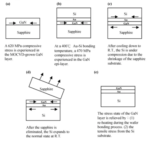
As mentioned in the experimental section, to transfer the GaN epilayer onto a Si wafer, the MOCVD-grown GaN epilayer goes through a series of thermal treatments. Thus, the GaN epilayer experiences different stress states during the fabrication process of the thin-GaN LED structure. Fig. 2 shows the evolution of the GaN epilayer during the substrate transfer process. According to Kozawa’s result, the GaN epilayer grown on the sapphire substrate has a compressive stress of approximately 620 MPa at a thickness of 4 m [30]. We have previously mentioned that the 620 MPa compressive stress includes two contributions: (1) the lattice constant mismatch and (2) the CTE mismatch between the GaN layer and the sapphire substrate. The thermal stress induced by the CTE mismatch can be estimated by the following equation:
where (7.6 ppm/ C) and (5.6 ppm/ C) are the CTE values of the sapphire substrate and the GaN epilayer. is
approximately 975 C, and is Young’s modulus for GaN. Inserting these numbers into (1), a thermal stress of the as-grown GaN epilayer of 370 MPa was determined. The total compres-sive stress of the GaN epilayer is 620 MPa, so the comprescompres-sive stress induced by the lattice constant mismatch in the as-grown MOCVD GaN epilayer is approximately 250 MPa.
During the Au-Si wafer bonding process, GaN and Si wafers were heated up to 420 C. The temperature difference in (1) would be reduced to 575 C; hence, the compressive stress in the GaN epilayer was relieved by 150 MPa. In other words, when the GaN wafer was bonded with Si wafer at 420 C, the compressive stress level of the GaN epilayer was approximately 470 MPa. As the temperature of the bonded sapphire/GaN/Si samples cools down to room temperature, the stress of the GaN epilayer is mainly determined by the stress balance of the Si and sapphire wafers. The CTE values of sapphire substrate and that of GaN are larger than that of Si. Cooling down from the bonding temperature (420 C), the compression of the GaN epilayer and the sapphire substrate would be restrained by the bonded Si wafer. Therefore, at this stage, the GaN epilayer would gain very little compressive stress because of the presence of the bonded Si wafer. More-over, we should note that the Si wafer was under compression at this stage. Once the sapphire substrate was removed by the LLO process, the Si wafer would expand back to the normal state at room temperature. The expansion of the Si wafer provides a tensile force to reduce the compressive state of the GaN epilayer. The tensile force exerted on the GaN epilayer
by the Si substrate is expressed as: ,
where is the CTE of Si and C. Plugging in all the necessary parameters, the stress relieved by the tension of the Si substrate is approximately 235 MPa. Thus, the residual stress level in the transferred GaN epilayer on the Si substrate is approximately 235 MPa (470-235). Based on the above discussion, we conclude that the stress of the transferred GaN epilayer can be adjusted by the following two factors: (1) the bonding temperature, which relieves the thermal stress of the GaN epilayer on sapphire, and (2) the tension force provided by the smaller CTE transfer substrate, such as Si.
B. Raman Measurements
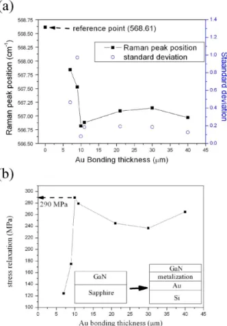
A common method to distinguish the strain/stress on the epi-taxial film is by measuring the bound-exciton transition energy levels and resonance enhancement of the anti-Stokes photolu-minescence as reported for GaN films grown on sapphire or Si(111) substrates [31]–[33]. Kozawa et al. used the shift of the Raman peak position to investigate the stress level of the GaN layer. It is reasonable that Kozawa correlated the stress level of the GaN epilayer with the measured Raman shift ac-cording to the following relationship: . With this relationship, we can analyze the stress state of the GaN epi-layer using the Raman spectrum of the GaN epiepi-layer. Fig. 3(a) shows the Raman peak position versus various bonding layer thicknesses ranging from 7 m to 40 m. The Raman peak po-sition of the initial GaN layer on sapphire was determined to be 568.61 cm . We found that the Raman peak position of the GaN epilayer red-shifted to the short wave-number region after the transfer onto the Si substrate. In Kozawa’s analysis, the red shift implies relief of the compressive stress state in the
Fig. 2. The evolution of the GaN epilayer during the substrate transfer process.
GaN epilayer. Using Kozawa’s relationship, , the stress level of the transferred GaN epilayer with different Au bonding thicknesses can be obtained. Fig. 3(b) shows the magnitude of the compressive stress relief vs. the Au bonding layer thickness. The minimum residual compressive stress in the transferred GaN thin film occurred at the largest Raman peak po-sition shift of 10 m for the Au layer (red shift, 1.79 cm ). The maximum compressive stress relief is approximately 290 MPa. This value is less than half of the reported value of the as-grown GaN epilayer. The relief of the compressive stress of the trans-ferred GaN layer can be mainly attributed to the replacement of the initial grown sapphire substrate by the Si substrate. Based on the previous discussion, we determined that the stress relief by the layer-transfer process is approximately 385 MPa. However, the stress relief at the 7 m Au thickness is only approximately 125 MPa in our Raman spectrum. Therefore, we realize that the effect of the Au bonding layer on the stress-state of the GaN layer cannot be ignored. We believe that the Au bonding layer has two effects on the stress-state of the GaN epilayer during the process of transferring the GaN epilayer. The first effect is the thermal stress effect contributed by the Au bonding layer. The CTE of Au ( C) is much larger than that of GaN ( C), so the Au bonding layer can also cause com-pressive stress in the GaN epilayer after the sapphire substrate is removed. Therefore, the Au bonding layer could exert a com-pressive stress on the GaN epilayer during the cooling after the wafer bonding process. The structure will bend toward the Au layer, as depicted in Fig. 4, where is the radius of curvature, L is the length, W is the width, and t is the thickness of the layer. The stress distribution for heteroepitaxial structures can be
for-mulated by using the following equations for the force balance, momentum balance, and equal lattice constants at the interface:
We combine these equations and thus obtain the modified Stony’s equation.
where is the Poisson’s ratio. Furthermore, we divided the discuss of the Au layer into two parts. In the first part, we dis-cuss the stress of Au induced by Si. We simplify the equation to , in which the strain of Si is proportional to the thickness of the Au layer square. Because the ratio of the Au thickness to the Si thickness is very small, we infer that the Si substrate hardly deforms. The curvature in this system shows a slight change. In the second part, we observed the stress of GaN induced by Au. Similarly, we can obtain from the modified Stony’s equation. In this equation, Y and are constants while the curvature, , is also a constant in the discussion of case 1. The stress of GaN induced by Au can be neglected because it will
374 JOURNAL OF DISPLAY TECHNOLOGY, VOL. 9, NO. 5, MAY 2013
Fig. 3. (a) The Raman peak position and (b) the stress relaxation versus various bonding Au layer thickness ranging from 7 m to 40 m at 420 C.
Fig. 4. The illustration of GaN on Si with Au-Si bonding.
be only affected by Si substrate when the Au is extremely thin. When the Au thickness increases, a thickness effect occurs, and the stress of GaN is a function of the Au thickness square. We can observe a quadratic curve when the Au bonding layer is over 10 m. However, at the initial Au bonding thickness, we found that the stress relief increased with the Au thickness. We believe that the second function of the buffering effect plays a dominant role in the compressive stress in the GaN layer. Au has the best ductility among all metal elements. Thus, the Au layer could serve as a buffer layer. We believe that the Au bonding layer could absorb the thermal stress caused by the sapphire during the wafer bonding and LLO process. The thicker the Au bonding layer becomes, the more the residual
stress level on the transferred GaN epilayer is relieved. When the Au bonding thickness ranges from 10 m to 40 m, the thermal stress effect becomes the dominant factor. With a thicker Au layer, the buffer is saturated. The stress level of the GaN epilayer was mainly influenced by the thermal stress from the Au layer. When the Au layer is at 10 m, the stress relief reaches its maximum. This leads to the optimal balance between the buffering and thermal stress effects.
Next, a 2-D mapping scan of the Raman examination is used to observe the transferred GaN surface stress state. The de-tailed Raman peak image is measured, and the standard devi-ation can be calculated. Based on the previous discussion, we understand that the larger the standard deviation of the mea-sured Raman peak shift, the higher vibration of the stress state in the GaN layer. This implies that the quality of the GaN sur-face is worse. The hollow circles in Fig. 3(a) show the stan-dard deviation of the measured Raman peak position versus the Au bonding layer thickness. The tendency shows that the values of the standard deviation become higher while the bonding Au thickness becomes thinner. The values become small when the bonding Au thickness is over 10 m. This means that the trans-ferred GaN epilayer has a better film quality with a thicker Au bonding layer. Two effects degrade the quality of the GaN epi-layer after the epi-layer transfer process: (1) micro-cracks during the LLO process, and (2) the rough n-GaN surface induced by the LLO process. The micro-cracks in the GaN epilayer most likely will result from the high local temperature at the GaN/sapphire interface during laser separation. A thicker Au layer could pre-vent the formation of those micro-cracks due to its buffering ef-fect and better thermal conduction, which avoids high local tem-perature accumulation at the GaN/sapphire interface. Another possible explanation for this behavior is that the Au-Si bonding layer will form many craters and voids owing to the quick disso-lution of Au atoms into Si. In Bokhonov’s study, a large amount of Au atoms will dissolve into Si after long reaction durations, forming craters and voids [34]. These craters and voids that form under the GaN thin film will cause the transferred GaN layer to cave in. The caved-in GaN surface creates a non-mirror face and increases the variation of the Raman peak position due to layer stress fluctuations. In our experiments, the thicker Au layer was not completely consumed, so the craters and voids were not easily formed. In addition, we can observe that micro-cracks might be induced by the LLO process by different mapping sults in the same sample. Fig. 5(a) is the Raman mapping re-sult for the smooth GaN surface, and Fig. 5(b) corresponds with cracks on the GaN surface. The deeper yellow regions in the second figure indicate that the Raman peak position is lower. In other words, a larger compressive stress is relieved. The same result is observed on other samples. We believe that the cracks induced by LLO will help relieve the compressive stress al-though they will degrade the film quality as well. The result that the crack will lead to the worse film quality will degrade the lighting efficiency of the LED.
C. Stress Change at Different Bonding Temperatures
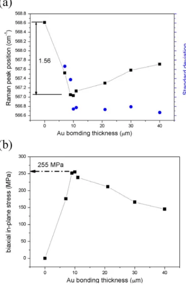
To verify the nature of the stress evolution, we repeated the experiments under a different bonding temperature of 380 C and also measured the in-plane biaxial stress on the transferred GaN layer. Fig. 6 shows the Raman peak position versus the Au
Fig. 5. Raman mapping result on transferred GaN surface: (a) smooth surface (b) cracks.
Fig. 6. (a) The Raman peak position and (b) the stress relaxation versus various Au bonding layer thicknesses ranging from 7 m to 40 m at 380 C.
bonding layer for a comparison with Fig. 3. We note the same tendency but a lower Raman peak shift of approximately 1.56 cm . Moreover, a lower amount of compressive stress relief, 255 MPa, can be obtained. This value is slightly smaller than 290 MPa, which is what is relieved when the bonding temper-ature is at 420 C. This result agrees with the deduction in Part
A. A lower bonding temperature results in two effects that re-duce the compressive stress relief. One effect is inre-duced by sap-phire during the heating process, while the other is induced by Si during the cooling process. In the beginning, the compressive stress in the GaN epilayer will be relieved by 150 MPa due to the relief of the thermal stress in the heating process. The value decreases to 134 MPa at the lower bonding temperature. In con-trast, the tension force induced by the expansion of the Si wafer during the cooling process will also decrease, from 235 MPa to 211 MPa. For the above two reasons, we obtained a lower com-pressive stress relief at the lower temperature and confirm that we change the biaxial in-plane stress by controlling the temper-ature of the process.
IV. CONCLUSION
Transferred GaN films on Si substrates were characterized by Raman spectroscopy measurements, and the residual stress state level was also calculated. The transferred GaN films were found to be strained by the biaxial compressive stress. A 10 m Au bonding layer thickness was proven to have the lowest residual compressive stress by observing the measured strain and the shift of the Raman peak. Finally, we changed the biaxial in-plane stress of the transferred GaN thin film by controlling the bonding conditions, including the bonding layer thickness and the bonding temperature.
REFERENCES
[1] S. Nakamura, Y. Harada, and M. Seno, “Novel metalorganic chemical vapor deposition system for GaN growth,” Appl. Phys. Lett., vol. 58, p. 2021, 1991.
[2] S. Nakamura, M. Senoh, and T. Mukai, “High-power lnGaN/GaN double-heterostructure violet light emitting diodes,” Appl. Phys. Lett., vol. 62, p. 2390, 1993.
[3] N. Tansu, H. Zhao, G. Liu, X.-H. Li, J. Zhang, H. Tong, and Y.-K. Ee, “III-nitride photonics,” IEEE Photon. J., vol. 2, pp. 241–248, 2010. [4] S. T. Tan, X. W. Sun, H. V. Demir, and S. P. DenBaars, “Advances
in the LED materials and architectures for energy-saving solid-state lighting toward lighting revolution,” IEEE Photon. J., vol. 4, pp. 613–619, Apr. 2012.
[5] R. M. Farrell, E. C. Young, F. Wu, S. P. DenBaars, and J. S. Speck, “Materials and growth issues for high-performance nonpolar and semipolar light-emitting devices,” Semiconductor Sci. and Technol., vol. 27, p. 024001, 2012.
[6] H. Zhao, G. Liu, J. Zhang, J. D. Poplawsky, V. Dierolf, and N. Tansu, “Approaches for high internal quantum efficiency green InGaN light-emitting diodes with large overlap quantum wells,” Opt. Expr., vol. 19, no. S4, pp. A991–A1007, 2011.
[7] J. Zhang and N. Tansu, “Improvement in spontaneous emission rates for InGaN quantum wells on ternary InGaN substrate for light-emitting diodes,” J. Appl. Phys., vol. 110, p. 113110, 2011.
[8] G. Liu, H. Zhao, J. Zhang, J. H. Park, L. J. Mawst, and N. Tansu, “Selec-tive area epitaxy of ultra-high density InGaN guantum dots by diblock copolymer lithography,” Nanoscale Res. Lett., vol. 6, p. 342, 2011. [9] H. P. Zhao, G. Y. Liu, X.-H. Li, R. A. Arif, G. S. Huang, J. D.
Poplawsky, S. T. Penn, and N. Tansu, “Design and characteristics of staggered InGaN quantum-well light-emitting diodes in the green spectral regime,” IET Optoelectron., vol. 3, pp. 283–295, 2009. [10] H. Zhao and N. Tansu, “Optical gain characteristics of staggered InGaN
quantum wells lasers,” J. Appl. Phys., vol. 107, p. 113110, 2010. [11] J. Zhang, H. Zhao, and N. Tansu, “Large optical gain
AlGaN-delta-GaN quantum wells laser active regions in mid-and deep-ultra-violet spectral regimes,” Appl. Phys. Lett., vol. 98, p. 171111, 2011. [12] H. Zhao, J. Zhang, G. Liu, and N. Tansu, “Surface plasmon
disper-sion engineering via double-metallic Au/Ag layers for III-nitride based light-emitting diodes,” Appl. Phys. Lett., vol. 98, p. 151115, 2011. [13] H. Zhao, G. Liu, R. A. Arif, and N. Tansu, “Current injection
effi-ciency induced effieffi-ciency-droop in InGaN quantum well light-emitting diodes,” Solid-State Electron., vol. 54, pp. 1119–1124, 2010.
376 JOURNAL OF DISPLAY TECHNOLOGY, VOL. 9, NO. 5, MAY 2013
[14] H. J. Kim, S. Choi, S.-S. Kim, J.-H. Ryou, and P. D. Yoder, “Im-provement of quantum efficiency by employing active-layer-friendly lattice-matched InAlN electron blocking layer in green light-emitting diodes,” Appl. Phys. Lett., vol. 96, p. 101102, 2010.
[15] Y.-K. Ee, J. M. Biser, W. Cao, H. M. Chan, R. P. Vinci, and N. Tansu, “Metalorganic vapor phase epitaxy of III-nitride light-emitting diodes on nanopatterned AGOG sapphire substrate by abbreviated growth mode,” IEEE J. Sel. Topics Quantum Electron., vol. 15, no. 4, pp. 1066–1072, Jul./Aug. 2009.
[16] Y.-K. Ee, X.-H. Li, J. Biser, W. Cao, H. M. Chan, R. P. Vinci, and N. Tansu, “Abbreviated MOVPE nucleation of III-nitride light-emitting diodes on nano-patterned sapphire,” J. Cryst. Growth, vol. 312, pp. 1311–131, 2010.
[17] Y. Li, S. You, M. Zhu, L. Zhao, and W. Hou, “Defect-reduced green GaInN/GaN light-emitting diode on nanopatterned sapphire,” Appl.
Phys. Lett., vol. 98, p. 151102, 2011.
[18] X.-H. Li, R. Song, Y.-K. Ee, P. Kumnorkaew, J. F. Gilchrist, and N. Tansu, “Light extraction efficiency and radiation patterns of III-nitride light-emitting diodes with colloidal microlens arrays with various as-pect ratios,” IEEE Photon. J., vol. 3, no. 3, p. 489, Jun. 2011. [19] Y.-K. Ee, P. Kumnorkaew, R. A. Arif, H. Tong, J. F. Gilchrist, and N.
Tansu, “Light extraction efficiency enhancement of InGaN quantum wells light-emitting diodes with polydimethylsiloxane concave mi-crostructures,” Opt. Expr., vol. 17, p. 13747, 2009.
[20] J. J. Wierer, A. David, Jr., and M. M. Megens, “III-nitride photonic-crystal light-emitting diodes with high extraction efficiency,” Nature
Photon., vol. 3, pp. 163–169, 2009.
[21] A. Sztein, H. Ohta, J. Sonoda, A. Ramu, J. E. Bowers, S. P. DenBaars, and S. Nakamura, “GaN-based integrated lateral thermoelectric device for micro-power generation,” Appl. Phys., vol. 109, p. 053706, 2011. [22] J. Zhang, H. Tong, G. Liu, J. A. Herbsommer, G. S. Huang, and N.
Tansu, “Characterizations of seebeck coefficients and thermoelectric figures of merit for AlInN alloys with various In-contents,” J. Appl.
Phys., vol. 109, p. 053706, 2011.
[23] B. N. Pantha, I.-W. Feng, K. Aryal, J. Li, J.-Y. Lin, and H.-X. Jiang, “Erbium-doped AlInGaN alloys as high-temperature thermoelectric materials,” Appl. Phys. Express, vol. 4, p. 051001, 2011.
[24] W. S. Wong and T. Sands, “In Ga N light emitting diodes on Si substrates fabricated by Pd-In metal bonding and laser lift-off,” Appl.
Phys. Lett., vol. 77, p. 2822, 2000.
[25] H. K. Cho, S.-K. Kim, D. K. Bae, B.-C. Kang, J. S. Lee, and Y.-H. Lee, “Laser liftoff GaN thin-film photonic crystal GaN-based light-emitting diodes,” IEEE Photon. Technol. Lett., vol. 20, no. 12, pp. 2096–2098, Dec. 2008.
[26] A. David, T. Fujii, B. Moran, S. Nakamura, and S. P. DenBaars, “Pho-tonic crystal laser lift-off GaN light-emitting diodes,” Appl. Phys. Lett., vol. 88, p. 133514, 2006.
[27] M. H. Doan, S. Kim, J. J. Lee, H. Lim, and F. Rotermund, “Influence of laser lift-off on optical and structural properties of InGaN/GaN vertical blue light emitting diodes,” AIP Adv., vol. 2, p. 022122, 2012. [28] A. Bykhovski, B. Gelmont, M. Shur, and A. Khan, “Current-voltage
characteristics of strained piezoelectric structures,” J. Appl. Phys., vol. 77, p. 1616, 1995.
[29] S. C. Hsu and C. Y. Liu, “Fabrication of thin-GaN LED structures by Au-Si wafer bonding,” Electrochem. and Solid-State Lett., vol. 9, pp. G171–G173, 2006.
[30] T. Kozawa, T. Kachi, H. Kano, H. Nagase, N. Koide, and K. Manabe, “Thermal stress in GaN epitaxial layers grown on sapphire substrates,”
J. Appl. Phys., vol. 77, p. 4389, 1995.
[31] V. Y. Davydov, N. S. Averkiev, I. N. Goncharuk, D. K. Nelson, I. P. Nikitina, A. S. Polkovnikov, A. N. Smirnov, M. A. Jacobson, and O. K. Semchinova, “Raman and photoluminescence studies of biaxial strain in GaN epitaxial layers grown on 6H-SiC,” J. Appl. Phys., vol. 82, p. 5097, 1997.
[32] G. Attolini, L. Francesio, P. Franzosi, C. Pelosi, S. Gennari, and P. P. Lottici, “Raman scattering study of residual strain in GaAs/InP het-erostructures,” J. Appl. Phys., vol. 75, p. 4156, 1993.
[33] S. K. Tripathy, G. Xu, X. Mu, Y. J. Ding, M. Jamil, R. A. Arif, N. Tansu, and J. B. Khurgin, “Phonon-assisted ultraviolet anti-Stokes photolumi-nescence from GaN film grown on Si(111) substrate,” Appl. Phys. Lett., vol. 93, p. 201107, 2008.
[34] B. Bokhonov, “Nanocrystalline powder formation during mechanical alloying of W and Si,” J. Alloys and Compounds, vol. 199, no. 125, 1993.
Bo-Wen Lin, photograph and biography not available at the time of publication.
Nian-Jheng Wu, photograph and biography not available at the time of publication.
Yew Chung Sermon Wu, photograph and biography not available at the time of publication.