行政院國家科學委員會專題研究計畫 成果報告
前瞻奈米壓印技術運用於 InGaN 量子點的選擇性生長與光 電元件之相關應用
計畫類別: 個別型計畫
計畫編號: NSC93-2215-E-006-034-
執行期間: 93 年 08 月 01 日至 94 年 10 月 31 日 執行單位: 國立成功大學微電子工程研究所
計畫主持人: 莊文魁
計畫參與人員: 莊文魁,張育聖,屈岳杰,杜文杰
報告類型: 精簡報告
報告附件: 出席國際會議研究心得報告及發表論文 處理方式: 本計畫可公開查詢
中 華 民 國 94 年 12 月 27 日
行政院國家科學委員會專題研究計畫 成果報告
前瞻奈米壓印技術運用於 InGaN 量子點的選擇性生長與光電元件之相關應用
I. Growth and characterization of gallium nitride nanowires by catalyst-assisted chemical vapor deposition
Abstract --- The preparation of high-purity gallium nitride nanowires is accomplished by a catalytic growth using gallium and ammonia. A series of experiments involving catalyst selection and different reaction parameters were applied to systematically optimize and control the vapor-liquid-solid (VLS) growth of the nanowires. The X-ray diffraction (XRD), scanning electron microscopy (SEM) and energy-dispersive spectroscopy (EDS) were used to characterize the samples. The resulting nanowires, which are several micrometers in length and 80-100 nm in diameters, are predominantly in GaN wurtzite phase. This work opens up an exciting opportunity for detailed studies of the fundamental properties and potential applications of semiconductor nanowires.
Keywords: Gallium nitride (GaN), nanowires, vapor-liquid-solid (VLS) growth, SEM, EDS
INTRODUCTION
Recent progress in the synthesis and characterization of one dimensional nanostructures has been greatly advanced to an unimaginable level. As the understanding of the novel physical properties of one-dimensional nanoscale materials becomes deepen, the potential applications in constructing nanoscale electronic and optoelectronic devices [1] are no longer just a science fiction, but a realized dream.
The GaN, one of important III-V semiconductors with a wurtzite structure and direct band-gap of 3.4eV, is an ideal material for uses as UV or blue light emitting diodes, photodetectors, high-speed field-effect transistors, and high temperature/power electronic devices [2]. In fact, the extensive device applications of GaN-related materials have prompted many researchers to make every endeavor to study the behaviors of low dimensional GaN-based nanostructures such as nanowires and quantum dots [3]. Nowadays, the synthesis of GaN nanowires has already been achieved by various techniques such as carbon nanotube assistant reaction [4], laser ablation [5], and catalytic assistant chemical vapor deposition [6-7]. In particular, a large number of crystalline GaN nanowires have been obtained by a catalytic synthesis based on a vapor-liquid-solid (VLS) growth mechanism [4, 7]. Previous reports indicated that a large-scale synthesis of GaN nanowires could be derived from the catalytic growth using Ni or Au as catalyst [8-9]. In our present work, we also use Ni and Au to propel the GaN nanowire growth. In our initial experiments, the purity and diameters of nanowires were difficult to control effectively; however, not until recently the successful breakthroughs finally allowed us to achieve high quality GaN nanowires. In these experiments, the growth conditions including growth temperature, NH 3 flow rate and total reaction time are modified judiciously.
Based on the comparison of our previous results, we summarize the optimum growth parameters and then give analyses of XRD and EDS measurements [10].
EXPERIMENTS A. Source and Substrate
The (100) silicon substrates were respectively cleaned via ultrasonic vibration means in solutions of 30% HCl, acetone, isopropanol and deionized water, with 3 minutes in each step before use. Next, ultrahigh quality molten gallium (99.9999%) and NH 3 gas (99.9997%) were prepared in advance for further nanowire growth in a horizontal tube reactor.
B. Catalyst Preparation
Two different catalysts involving Ni and Au particles were separately applied to substrate B (see Figure
1) for growth comparison. The Au catalyst with a typical thickness of several nanometers was deposited on
the substrate via sputtering. On the other hand, the Ni catalyst was dispersed instead by spin coating 0.01M
Ni(NO 3 ) 2 solution on the silicon substrate.
C. Growth of GaN Nanowires
The experimental setup for GaN nanowire growth is described schematically in Figure 1. Substrate B (5 x 5 mm 2 ) deposited with Au or Ni catalyst was placed in a 3-inch quartz tube at a distance of 5 cm away from crucible A containing enough amount of molten gallium (1g) locate at the center of a tube furnace. The quartz tube was degassed first and the background pressure of the tube was subsequently brought down to about 5 x 10 −3 torr. Next, high purity Ar was introduced into the tube as an ambient gas while the heating was taking place inside the furnace. The temperature of the furnace was increased at a rate of 25-30°C/min from room temperature to a typical reaction temperature of 800-950 °C and kept it for 2-7h under a steady NH 3 flow at a rate of 20-50 sccm. After the reaction was completed, the furnace was then cooled down to room temperature and the resulting nanowires were collected from the surface of substrate B.
Figure 1. Schematic of experimental setup for the growth of GaN nanowires. Gallium and catalyst are placed in crucible A and substrate B, respectively.
D. Morphology and Structure Characterization
The morphologies of the resulting material on substrate B were observed using scanning electron microscopy (SEM). Further stoichiometry and structural analyses of resulting nanowires were analyzed using X-ray diffraction (XRD) and energy-dispersive spectroscopy (EDS).
(100) (101) (321) (102) (110) (103) (200) (112) (210)
950℃ NH
3:20sccm
950 ℃ NH3:50sccm
(a) (b)
Figure 2. (a) XRD diagram of GaN nanowires. The sample was prepared under the conditions described in the figure. (b) A representative result of EDS measurement. The sample was prepared under conditions described in the figure.
RESULTS AND DISCUSSION
The overall crystal structures of nanowires were studied by XRD analysis, which shows completely
uniform hexagonal wurtzite GaN phase. Figure 2(a) depicts a XRD pattern of synthesized GaN nanowires at
conditions of 950°C , NH3 flow rate of 20 sccm, and the reaction time of 5hr. The diffraction peaks of (1 0
0), (0 0 2), (1 0 1), (3 2 1), (1 0 2), (1 1 0), (1 0 3), (2 0 0), (1 1 2) and (2 1 0) correspond to the hexagonal
wurtzite GaN with lattice constants of a = 0.318 and c = 0.518 nm, which agree well with the reported values
of bulk GaN crystals. The strong diffraction peaks relative to the background signals clearly suggest the
resulting GaN nanowires do possess a highly pure GaN wurtzite phase. Figure 2(b) exhibits the result of
EDS measurement. The growth conditions were set at 950 °C, NH 3 flow rate of 50 sccm, and the reaction
time of 3hr. Notice that the percentage of detected oxygen is too high in this figure and the atomic
percentage ratio of gallium to nitrogen is not 1 to 1 as expected. One plausible reason for this observation
might possibly be due to the inevitable presence of oxygen inside the tube causing the surface oxidation and
the subsequent formation of Ga 2 O 3 on the surface of substrate B. In addition, the noticeably high percentage
of nitrogen indicates that in a large part the resulting nanowires thus produced is indeed made up of GaN.
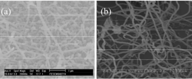
Some modifications from the previous setup were made to improve the purity, morphology and uniformity of GaN nanowires. The experimental parameters were chosen by holding the reaction time and the distance from Ga source to substrate constant, while setting the reaction temperature and NH 3 flow rate in the neighborhoods of 800-950 °C and of 20-50 sccm, respectively. Figure 3 presents SEM images for nanowire samples obtained at different conditions. The GaN nanowires are around 100 nm in diameter and from several to tens of micrometers in length. In addition, the nanowires thus grown also comparably demonstrate a smooth surface and a little or no ramification over their lengths. In terms of catalyst selection, the fruitful results were generated using Ni as catalyst over Au. The resultant SEM images are shown in Figure 4. In fact, as the identical growth condition are maintained while selecting Ni as a catalyst, a highly concentrated density of GaN nanowires with each wire comparably longer in length and a reduced diameter of around 80 nm could be successfully obtained in return.
(a) (b)
Figure 3. SEM images of resultant samples heated for 5 hr. at respective growth temperature and NH 3 flow rate of (a) 920°C and 50 sccm, and (b) 950°C and 20sccm.
(a) (b)
Figure 4. SEM images of nanowire samples achieved with different catalysts of (a) Au and (b) Ni.
CONCLUSIONS
In summary, large-scale hexagonal wurtzite GaN nanowires with diameters between 80 and 100 nm and lengths up to tens of micrometers were formed by catalyst-assisted chemical vapor deposition of metal gallium vapor with ammonia flowing at the rate of 20-50 sccm in a horizontal oven at 800–950 °C. The best temperature and NH 3 flow rate for growing GaN nanowires are about 920 °C and 20 sccm, respectively. We are currently studying other factors which influence the growth of these cylindrical nanostructures, including pressure, carrier gas, and sample location, as well as trying to gain a better understanding of detailed growth mechanism involved.
REFERENCES
[1] J. T. Hu, T.W. Odom, and C.M. Lieber, Acc. Chem. Res., 32, (1999) 435.
[2] X. Peng, L. Manna, W. Yang, J. Wickham, E. Scher, A. Kadavanich, A. P. Alivisatos, Nature, 404, (2000) 59-61.
[3] F. A. Ponce and D. P. Bour, Nature, 386, (1997) 351-359.
[4] W. Han, S. Fan, Q. Li, and Y. Hu, Science, 277, (1997) 1287-1289.
[5] X. F. Duan and C. M. Lieber, J. Am. Chem. Soc., 122, (2000) 188-189.
[6] L. Yang, C. S. Xue, C. M. Wang, and H. X. Li, Nanotechnology, 14, (2003) 50.
[7] C. -C. Chen, C. -C. Yeh, Adv. Mater., 12, (2000) 738-741.
[8] Weiqiang Han, Shoushan Fan, Qunqing Li, and Yongdan Hu, Science, 277 (29), (1997) 1287.
[9] C. -C. Chen, C. -C.Yeh, C. -H. Chen, M. -Y. Yu, H. -L. Liu, J. -J. Wu, K. -H. Chen, L. -C. Chen, J. -Y.
Peng, and Y. -F. Chen, J. Am. Chem. Soc., 123(12), (2001) 2791-2798.
[10] Li Yang, Xing Zhang, Ru Huang, Guoyan Zhang, and Chengshan Xue, Physica E, 28 (3), (2005) 237-241.
II. Growth of InGaN self-assembled quantum dots and their application to photodiodes
Abstract --- Nanometer-scale InGaN self-assembled quantum dots (QDs) have been prepared by growth interruption, during metalorganic chemical vapor deposition growth. With a 12 s growth interruption, we successfully formed InGaN QDs with a typical lateral size of 25 nm and an average height of 4.1 nm. The QD density was about 2 × 10 10 cm − 2 . In contrast, much larger InGaN QDs were obtained without growth interruption. InGaN metal-semiconductor-metal photodiodes with and without QDs were also fabricated. It was found that the QD photodiode with lower dark current could operate in the normal incidence mode, and exhibit a stronger photoresponse.
Keywords: GaN/InGaN, MSM photodetectors, quantum dot (QD), MOCVD, PL, AFM
INTRODUCTION
III–V nitride semiconductor materials have a wurtzite crystal structure and a direct energy band gap. At room temperature, the band gap energy of AlInGaN varies from 0.7 to 6.2 eV depending on its composition.
Therefore, III–V nitride semiconductors are particularly useful for light-emitting devices and photodetectors in this wavelength region. Indeed, III–V nitride-based blue and green high brightness light-emitting diodes (LEDs) [1-2] made from InGaN/GaN quantum well (QW) structures are now commercially available for traffic light source and full color display. However, relatively few nitride-based blue/ultraviolet (UV) photodiodes could be found in the literature as compared to nitride-based LEDs. Blue/ultraviolet (UV) photodiodes are important devices that can be used in various commercial and military applications. For example, these devices can be applied in space, medical, and environmental fields. Currently, light detection in the blue/UV region still uses Si photodiodes. However, since room temperature band gap energy of Si is only 1.2 eV, the responsivity of Si photodiodes is low in the blue/UV region. With the advent of optoelectronic devices fabricated on wide direct band gap materials, it becomes possible to produce high performance solid-state photodiode arrays sensitive in the blue/UV region. Depending on device structure, nitride-based p-n junction diode [3], p-i-n diode [4-5], p- π -n diode [6], Schottky barrier detector [7], and metal-semiconductor-metal (MSM) photodiodes [8-10] could all be used to detect blue/UV signal. Among these devices, MSM photodiodes have an ultralow intrinsic capacitance and their fabrication process is also compatible with field-effect-transistor [FET]-based electronics. Thus, one can easily integrate GaN MSM photodetectors with GaN FET-based electronics to realize a nitride-based optoelectronic integrated circuit.
Low-dimensional carrier confinement nanostructures such as quantum wires and dots (or islands) are quite attractive for application to high-performance electronic and optical devices. Recently, it has been shown that nitride quantum dots (QDs) can be self-organized using the strain-induced Stranski–Krastanov growth mode [11-13]. It has also been shown that nitride QDs can be self-organized using growth interruption during metalorganic chemical vapor deposition (MOCVD) growth [14]. Although the successful fabrication of InGaN QDs has been reported by many research groups, very few reports of InGaN QD-based optoelectronic devices could be found in the literature [15-16]. In this article, we use MOCVD growth interruption to form nitride self-assembled quantum dots (SAQDs), InGaN QD MSM photodiodes were subsequently fabricated. The photoluminescence (PL) properties of InGaN QDs and the current–voltage (I –V) characteristics of fabricated MSM photodiodes will be discussed.
EXPERIMENTS
Samples used in this study were grown on (0001)-oriented sapphire (Al 2 O 3 ) substrates in a vertical
low-pressure MOCVD reactor with a high-speed rotation disk [17-18]. The gallium, indium and nitrogen
sources were trimethylgallium, trimethylindium, and ammonia, respectively. After a 30-nm thick
low-temperature GaN nucleation layer was deposited onto the sapphire substrate at 500 °C, the temperature
was raised to 1000 °C to grow a 2-μm-thick undoped GaN buffer layer. The growth temperature was then
reduced to 730 °C to grow InGaN QDs with growth rate of 0.04 nm/s. During the deposition of InGaN, an
interrupted growth method was employed in preparing sample A. In other words, we deposited a
1.2-nm-thick InGaN layer on top of the undoped GaN buffer layer, stopped the growth for 12 s, and then
deposited another 1.2-nm-thick InGaN layer so as to achieve a total InGaN layer thickness of 2.4 nm, as shown in Fig. 1 [14]. For comparison, sample B was prepared by directly depositing a 2.4-nm-thick InGaN layer on top of the GaN buffer layer, as also shown in Fig. 1. Furthermore, samples C and D without the QDs
Figure 1. Scheme showing the two growth methods of InGaN nanostructure samples.
were also prepared by depositing a 2.4-nm-thick and 100-nm-thick InGaN layer on top of the undoped GaN buffer layer, respectively. It should be noted that these four kinds of samples have the same average indium composition. Room temperature surface morphologies of the InGaN nanostructure samples were then characterized ex situ by an atomic force microscopy (AFM) system (Shimmadzu SPM-9500JZ) with a sharpened Si 3 N 4 tip. PL was also used to study the optical properties of these samples under room temperature. During PL measurements, a 325 nm He-Cd laser was used as the excitation source. The collected luminescence signal was dispersed by a monochromator, and detected by a photomultiplier tube (PMT). InGaN QD MSM photodiode was then fabricated on sample A as photodiode I. For comparison, 2 MSM photodiodes without QDs were fabricated on samples C and D as photodiodes II and III, respectively.
Figure 2 shows the schematic structure of the InGaN QD MSM photodiodes used in this study. The fabrication process of these InGaN MSM photodiodes was as follows. Prior to the deposition of contact
electrodes, wafers were dipped in a diluted hydrochloric acid water solution (HCl:H 2 O = 1:1) for 3 min to
Figure 2. Schematic structure of InGaN nanostructures MSM photodiode.
remove native oxides. A Ni layer was subsequently deposited onto the sample surface by e-gun evaporator to serve as the metal contact. Standard lithography and etching were then performed to define the interdigitated contact pattern. The fingers of the contact electrodes were 10 mm wide and 200 mm long with a spacing of 10 mm. The active area of the whole device was 200 × 200 mm 2 . Finally, Au layers were then deposited on top of the contact electrodes to serve as bonding pads. A HP-4155B semiconductor parameter analyzer was then used to measure the current–voltage (I –V) characteristics of these MSM photodiodes in dark and under illumination. For photocurrent measurements, a 150 mW gas Ar laser with 457, 465, 476, 488 and 514 nm lines, illuminating from the front side of the fabricated photodiodes, was used as the light source.
RESULTS AND DISCUSSION
Figures 3(a) and 3(b) show 500–500 nm 2 two dimensional (2D) AFM images of samples A and B,
respectively. As shown in Fig. 3(a), it can be seen that small circular InGaN SAQDs were formed by the interrupted growth mode. From these AFM pictures, it was found that the diameter of these circular QDs was in the range of 20–38 nm, with an average height of 4.1 nm. On the other hand, the density of these QDs was estimated to be around 2 × 10 10 cm −2 . In contrast to the small circular QDs observed from sample A, large oval InGaN islands were found in sample B without growth interruption. It was found that the longer width of these oval islands was around 140 nm while the shorter width was about 70 nm, with an average height of 1.7 nm. We also found that the density of these large oval islands was about 3.5 × 10 8 cm −2 . From these AFM pictures shown in Figs. 3(a) and 3(b), it can be seen clearly that by introducing the interrupted growth method, we could significantly change the surface morphology of the MOCVD grown InGaN samples. It
Figure 3. Two-dimensional 500–500 nm 2 AFM image of (a) sample A (with the smaller InGaN nanostructures, grown by the use of interrupted growth mode in MOCVD) and (b) sample B (with the larger InGaN nanostructures, grown without using the interrupted growth mode in MOCVD).
should be noted that the size of the nanostructures observed from sample A was much smaller than that observed from sample B. As a result, growth interruption could release the partial strain energy of InGaN epitaxial layer when InGaN was grown more than the critical thickness 0.8 nm [19], i.e., 1.2 nm > 0.8 nm, then continued growing another 1.2 nm of InGaN, we can realize the nanoscale and discrete SAQDs. Thus, we should be able to observe a more significant quantum confinement effect from sample A. Figure 4 shows the measured PL spectra for samples A, B and D. It can be seen that the PL peak position of sample 1 is
Figure 4. Room temperature PL spectra for samples A, B, and 100-nm-thick InGaN.
located at 2.645 eV while the PL peak position of sample 2 is located at 2.578 eV. It was also found that the
normalized PL intensity observed from sample 1 was 50% larger than that observed from sample 2. In other
words, the introduction of growth interruption would result in a PL blueshift as large as 67 meV. It should be
noted that the nominal thickness of InGaN epilayer of these two samples was the same (i.e., 2.4 nm), i.e.,
they had the same InGaN coverage. Hence we should attribute the huge PL blueshift to the lateral size effect
of nanostructures. It is well known that the subband transition energies will increase when the size of
nanostructure becomes smaller [20]. Thus, although the InGaN coverage was the same for samples A and B, we could observe a larger PL transition energy from sample A prepared with growth interrupt, since growth interrupt will result in a smaller nanostructure size. Furthermore, we can see that the sample A is about 180 times the normalized PL intensity of sample D. It is possible that sample D has no quantum structures like quantum wells or dots to confine the exitons which will be trapped by defects (e.g., threading dislocations) which results in the low probability of radiation recombination. Hence sample D showed weak PL intensity.
Figures 5(a) and 5(b) show photocurrent and dark current of InGaN MSM photodiodes I and II fabricated on samples A and C, respectively. It can be seen that photocurrent and dark current both increase slowly as the
Figure 5. Dark and illuminated I –V characteristics of MSM photodiodes on (a) InGaN QDs and (b) 2.5-nm-thick InGaN without QDs.
applied bias increases. With the same device size, it was found that photodiode I had slightly lower measured dark currents than photodiode II. On the other hand, it was found that the photocurrent observed from photodiode I was much larger than that observed from photodiode II. It should be noted that these photodiodes were illuminated normally. Due to the special structure for samples A and C having nanoscale QDs and thin film, respectively, we can treat the photodiodes I and II as a QD photodetector and a QW photodetector. As a result, for the sake of the polarization selection rules, QW (2.4-nm-thick InGaN) detectors which are not sensitive to radiation that is incident perpendicular to the QW, on the contrary, the QD detector can operate in the normal incidence mode showing better photoresponse [21]. Figure 6 shows photocurrent to dark current contrast ratio of these three photodiodes. With a 10.1 V applied bias, it was
Figure 6. Photocurrent to dark current contrast ratios (PC/DC) of the three fabricated photodiodes.
found that photocurrent to dark current contrast ratio equals 400, 11, and 31, respectively. The large
photocurrent to dark current contrast ratio observed from photodiode I could again be attributed to the
formation of nanoscale InGaN SAQDs by growth interruption. It is possible that InGaN QD as a good
quantum capture system will get more photogenerated carriers under such illumination (blue-green light),
hence the photocurrent easily increases when an external bias (electric field) was applied onto the device. On
the other hand, the 100-nm-thick InGaN could merely provide less effective photogenerated carriers under
illumination, exhibiting poor photoelectric performance. As a result, we could observe a larger
photoresponse from photodiodes with InGaN nanostructures.
CONCLUSIONS
In summary, it has been demonstrated that we can use interrupted growth method in MOCVD to fabricate InGaN SAQDs. With a 12 s growth interruption, we successfully formed InGaN QDs with a typical lateral size of 25 nm and an average height of 4.1 nm. The QD density was about 2 × 10 10 cm −2 . In contrast, much larger InGaN nanostructures were obtained without growth interruption. InGaN MSM photodiodes with and without QDs were also fabricated. It was found that the InGaN QD photodiode with lower dark current can operate in the normal incidence mode. We could achieve a much larger photocurrent to dark current contrast ratio from MSM photodiodes with nanoscale InGaN SAQDs.
REFERENCES
[1] S. Nakamura, M. Senoh, N. Iwasa, and S. Nagahama, Jpn. J. Appl. Phys., Part 2 34, L797 (1995).
[2] W. C. Lai, S. J. Chang, M. Yokoyama, J. K. Sheu, and J. F. Chen, IEEE Photonics Technol. Lett. 13, 559 (2001).
[3] D. V. Kuksenkov, H. Temkin, A. Osinsky, R. Gaska, and M. A. Khan, J. Appl. Phys. 83, 2142 (1998).
[4] G. Parish, S. Keller, P. Kozodoy, J. A. Ibbetson, H. Marchand, P. T. Fini, S. B. Fleischer, S. P.
DenBaars, and U. K. Mishra, Appl. Phys. Lett. 75, 247 (1999).
[5] E. Monroy, M. Hamilton, D. Walker, P. Kung, F. J. Sa´nchez, and M. Razeghi, Appl. Phys. Lett. 74, 1171 (1999).
[6] A. Osinsky, S. Gangopadhyay, R. Gaska, B. Williams, M. A. Khan, D. Kuksenkov, and H. Temkin, Appl. Phys. Lett. 71, 2334 (1997).
[7] S. L. Rumyantsev, N. Pala, M. S. Shur, R. Gaska, M. E. Levinshtein, V. Adivarahan, J. Yang, G. Simin, and M. Asif Khan, Appl. Phys. Lett. 79, 866 (2001).
[8] D. Walker, E. Monroy, P. Kung, J. Wu, M. Hamilton, F. J. Sanchez, J. Diaz, and M. Razeghi, Appl.
Phys. Lett. 74, 762 (1999).
[9] Y. K. Su, Y. Z. Chiou, F. S. Juang, S. J. Chang, and J. K. Sheu, Jpn. J. Appl. Phys., Part 1 40, 2996 (2001).
[10] C. H. Chen, S. J. Chang, Y. K. Su, G. C. Chi, J. Y. Chi, C. A. Chang, J. K. Sheu, and J. F. Chen, IEEE Photonics Technol. Lett. 13, 848 (2001).
[11] B. Damilano, N. Grandjean, S. Dalmasso, and J. Massies, Appl. Phys. Lett. 75, 3751 (1999).
[12] K. Tachibana, T. Someya, and Y. Arakawa, Appl. Phys. Lett. 74, 383 (1999).
[13] C. Adelmann, J. Simon, G. Feuillet, N. T. Pelekanos, and B. Daudin, Appl. Phys. Lett. 76, 1570 (2000).
[14] L. W. Ji, Y. K. Su, S. J. Chang, L. W. Wu, T. H. Fang, J. F. Chen, T. Y. Tsai, Q. K. Xue, and S. C.
Chen, J. Cryst. Growth 249, 144 (2003).
[15] K. Tachibana, T. Someya, and Y. Arakawa, Appl. Phys. Lett. 75, 2605 (1999).
[16] K. Tachibana, T. Someya, and Y. Arakawa, IEEE J. Sel. Top. Quantum Electron. 6, 475 (2000).
[17] Y. K. Su, S. J. Chang, C. H. Ko, J. F. Chen, W. H. Lan, W. J. Lin, Y. T. Cherng, and J. Webb, IEEE Trans. Electron Devices 49, 1361 (2002).
[18] S. J. Chang, C. H. Kuo, Y. K. Su, L. W. Wu, J. K. Sheu, T. C. Wen, W. C. Lai, J. F. Chen, and J. M.
Tsai, IEEE J. Sel. Top. Quantum Electron. 8, 744 (2002).
[19] N. Grandjean and J. Massies, Appl. Phys. Lett. 72, 1078 (1998).
[20] P. Ball and L. Garwin, Nature (London) 355, 301 (1992).
[21] L. Chu, M. Arzberger, A. Zrenner, G. Bo¨hm, and G. Abstreiter, Appl. Phys. Lett. 75, 2247 (1999).
III. Highly responsive GaN metal-semiconductor-metal ultraviolet photodetectors with aluminum-doped zinc oxide and Ru/Ir based Schottky contacts
Abstract --- The fabrication and characterization of GaN interdigitated metal-semiconductor-metal
(MSM) ultraviolet (UV) photodetectors (PDs) have been successfully realized. The transparent
aluminum-doped zinc oxide (AZO) and Ruthenium (Ru)/iridium (Ir) based metallic layers were chosen as the
corresponding Schottky contacts. When using AZO as contact electrodes, the best current contrast ratio
(photocurrent to dark current) of 3.28 × 10 5 and the responsivity of 0.74 A/W were achieved for devices
annealed in N 2 ambient at 500 ° C and biased at 3V. For comparison, when binary Ru/Au or Ir/Au binary
metallic layers were used, the best achievable current contrast ratio and the responsivity became 9.48×10 5
(annealed at 500 ° C in O 2 ambient) and 1.99×10 − 1 A/W (as-deposited), for Ir/Au, 1.13×10 3 (annealed at
500 ° C in N 2 ambient) and 5.83×10 − 3 A/W (annealed at 500 ° C in N 2 ambient) were obtained instead,
respectively. Better device performance are attributable to highly transparent nature of AZO and the formation of RuO 2 having the corresponding work function higher than 5 eV which helps to lower the dark current. Finally, for a given bandwidth of 500Hz, the corresponding noise equivalent power (NEP) and the normalized detectivity D* determined for devices with AZO (annealed at 600 ° C), Ru/Au (annealed at 500 ° C), and Ir/Au (annealed at 500 ° C) contacts were 1.93×10 − 14 W & 2.32 × 10 13 cmHz 0.5 W − 1 , 2.31×10 − 13 W &
1.94×10 12 cmHz 0.5 W − 1 , and 1.84×10 − 10 W & 2.43×10 9 cmHz 0.5 W − 1 , respectively.
Keywords: GaN, MSM photodetectors, responsivity, detectivity, noise equivalent power, ZnO, Ru, Ir
INTRODUCTION
In recent years, Gallium nitride and related compound materials have been intensively investigated.
Owing to its excellent properties, such as direct and wide band gap, high thermal conductivity, and high-saturated velocity, these materials can be used for various optoelectronic devices, namely, the light emitting diodes (LEDs), laser diodes (LDs) and ultraviolet (UV) photodetectors. Among them, GaN-based UV photodetectors are potentially useful in many commercial and military applications, such as space communications, ozone layer monitoring, flame detection, missile treat warning, furnace control, water purification, optical autocorrelators, UV radiation dosimetry, pollution monitoring and engine monitoring.
Up to now, various types of GaN-based photodetectors have already been reported [1-5] and among them, the metal-semiconductor-metal (MSM) photodetector structures uniquely rely on the planar configuration and are particularly suitable for monolithic integration with field effect transistors (FETs) using GaN/sapphire MMIC technology [6]. Besides, the lateral, planar structure of the MSM offers extremely low capacitance, which matches well with the requirements of large bandwidth and low-noise performance. In fact, the enhancement in the performance of MSM UV photodetectors is critically dependent upon the judicious selection of Schottky contacts with proper barrier heights. In addition, the transparency of the contact metal is also important since more photons will be absorbed by the semiconductor if the contact metal is transparent. Therefore, the aforementioned considerations led us to choose highly transparent aluminum-doped zinc oxide (AZO) as the metal contacts. The corresponding device performance was compared against the ones with Ru/Ir based binary metallic contacts in terms of the current contrast ratio and responsivity. The significance of the characterization results and a short summary will be elaborated and given afterward to conclude this report.
EXPERIMENTS
In this work, the detector samples were grown on c-plane sapphire by metal organic vapor phase epitaxy (MOVPE). The device consists of a 2.2μm thick undoped-GaN layer grown on a GaN buffered sapphire substrate. The use of a thick GaN layer helps to obtain a high quality photodetectors. After the growth, samples were annealed at 750 ℃ for 20 min in an N 2 atmosphere. The room temperature carrier concentration and electron mobility of the undoped-GaN epitaxial layer were 5.72×10 16 cm − 3 and >
300cm 2 /V-sec, respectively. Next, the samples were properly cleaned in the acidic and organic solvents to removed unwanted oxides and organic residues. The MSM interdigitated structures were then lithographically defined and patterned using techniques of electron-beam evaporation, RF/DC sputtering, and lift-off. The annealing of Schottky contacts were performed afterward in either oxygen or nitrogen ambient at elevated temperatures.
RESULTS AND DISCUSSION
For photocurrent measurements, a 150 W deuterium lamp illuminated from the front side of the
detectors was used as the UV light source and the Keithley 4200 semiconductor parameter analyzer was used
to measure the current-voltage (I-V) characteristics. All relevant measurements were made before and after
annealing these devices with different contact electrodes in either O 2 or N 2 ambient at elevated temperatures
for 20 minutes. The resultant current contrast ratio, responsivity, and other relevant electrical parameter
measurements were tabulated in Table 1. For comparison, similar measurements were also repeated for
devices fabricated with Ru/Au and Ir/Au electrodes and the corresponding results are shown in Table 2. In
Table 1, notice that the devices with AZO were biased only up to 3 volts instead, owing to the fact that
beyond 3 volts the current contrast ratio dropped significantly as result of fast rising in dark current. The
responsivity spectra for devices with AZO annealed at different temperatures in N 2 ambient are demonstrated
Type Φ B (eV)
Bn Current Ratio (Bias at 3V)
Responsivity (A/W) (Bias at 3V,
350nm)
as-deposited 0.59 1.84 1 None
400℃ N 2 0.81 1.50 1.04×10 4 0.74
500℃ N 2 0.91 1.41 3.28×10 5 0.26
600℃ N 2 0.86 1.70 7.62×10 4 0.66
Table 1. The current contrast ratio, responsivity, and other relevant electrical parameter measurements for MSM photodetectors with AZO contact electrodes annealed at different temperatures in N 2 ambient. The Φ B and n are Schottky barrier height and ideality factor, respectively.
Type Φ B (eV)
Bn Current Ratio (Bias at 5V)
Responsivity (A/W) (Bias at 5V,
350nm) as-deposited 0.73 1.62 9.72×10 3 1.99×10 −1
500℃ O 2 1.01 1.57 9.48×10 5 2.45×10 −2
Ru/Au
500℃ N 2 0.98 1.45 2.92×10 1 9.37×10 −5
as-deposited 0.76 1.55 3.25 2.85×10 −4
500℃ O 2 0.92 1.55 3.18×10 2 4.89×10 −4
Ir/Au
500℃ N 2 0.97 1.69 1.13×10 3 5.83×10 −3
Table 2. The current contrast ratio, responsivity, and other relevant electrical parameter measurements for MSM photodetectors with Ru/Au and Ir/Au contact electrodes annealed at different temperatures in O 2 or N 2 ambient. The Φ B and n are Schottky barrier height and ideality factor, respectively.
B300 350 400 450 500
10
-210
-110
0in Figure 1(a). The corresponding curves for detectors with Ru/Au annealed at 500°C in O 2 or N 2 ambient are also plotted in Figure 1(b) for comparison. The cut-off wavelengths for AZO-PDs and Ru/Au-PDs are 370 and 365 nm, respectively, making these detectors truly solar blind. The devices with AZO comparably have superior current contrast ratio and responsivity over their counterparts with Ru/Au and Ir/Au, however, detectors with Ru/Au has better low frequency characteristics. The results are due to the highly transparent nature of AZO film and the formation of RuO 2 with work function of greater than 5 eV, which translates to lower dark current.
400
OC
(a) (b)
Figure 1. The responsivity spectra of MSM photodetectors fabricated with (a) aluminum-doped ZnO (in N 2 ambient) and (b) Ru/Au contact electrodes annealed at different temperatures and ambient.
500
OC 600
OC
R e s pon siv ity (A /W )
Wavelength (nm)
3 00 40 0 50 0
1 0
-51 0
-41 0
-31 0
-21 0
-11 0
0R u A u a s -d e p o s ite d R u A u 5 0 0
OC O
2
R u A u 5 0 0
OC N
2Responsivity (A/W)
W a ve le n g th (n m )
As for the noise characteristics of MSM photodetectors deposited with AZO, Ru/Au, and Ir/Au as contact electrodes, the respective low frequency spectra are demonstrated in Figure 2. The low-frequency noise in MSM photodiodes is not normally just the 1/f-type noise, but shot noise and Johnson noise are also included. For a given bandwidth of 500Hz, the corresponding noise equivalent power (NEP) and the normalized detectivity D* determined for devices with AZO (annealed at 600°C), Ru/Au (annealed at 500°C), and Ir/Au (annealed at 500°C) contacts were 1.93×10 −14 W & 2.32× 10 13 cmHz 0.5 W −1 , 2.31×10 −13 W
& 1.94×10 12 cmHz 0.5 W −1 , and 1.84×10 −10 W & 2.43×10 9 cmHz 0.5 W −1 , respectively. Comparably speaking, devices with Ru/Au outperformed the ones with AZO in terms of low-frequency noise; the observations believably were due to the facts that PDs with Ru/Au had lower dark current compared to ones with AZO.
0
(a) (b)
Figure 2. The low frequency noise spectra of MSM photodetectors with (a) AZO, (b) Ru/Au, and Ir/Au, as contact electrodes.
REFERENCES
[11] G. Parish, S. Keller, P. Kozodoy, J. A. Ibbetson, H. Marchand, P. T.Fini, S. B. Fleischer, S. P.
DenBaars and U. K. Mishra, “High performance (Al,Ga)N-based solar-blind ultraviolet p-i-n detectors on laterally epitaxially overgrown GaN”, Appl. Phys. Lett., Vol.75, p.247, 1999.
[12] E. Monroy, M. Hamilton, D. Walker, P. Kung, F. J. Sánchez and M. Razeghi, “High quality visible-blind AlGaN p-i-n photodiodes”, Appl. Phys. Lett., Vol.74, p.1171, 1999.
[13] A. Osinsky, S. Gangopadhyay, R. Gaska, B. Williams, M. A. Khan, D. Kuksenkov and H. Temkin,
“Low noise p-π-n GaN ultraviolet photodetectors”, Appl. Phys. Lett., Vol.71, p.2334, 1997.
[14] S. L. Rumyantsev, N. Pala, M. S. Shur, R. Gaska, M. E. Levinshtein, V. Divarahan, J. Yang, G. Simin and M. Asif Khan, “Low-frequency noise in Al0.4Ga0.6N-based Schottky barrier photodetectors”, Appl.
Phys. Lett., Vol.79, p.866, 2001.
[15] C. H. Chen, S. J. Chang, Y. K. Su, G. C. Chi, J. Y. Chi, C. A. Chang, J. K. Sheu and J. F. Chen, “GaN metal-semiconductor-metal ultraviolet photodetectors with transparent indium-tin-oxide Schottky cContacts”, IEEE Photon. Technol. Lett., Vol.13, p.848, 2001.
[16] D. G. Parker and P. G. Say, “Indium tin oxide/GaAs photodiodes for millimetric-wave applications”, Electron. Lett., Vol.22, p.1266,1988.
1 1 100 1k 10k 100k
10
-3210
-3110
-3010
-2910
-2810
-27Noise power Density
(
A2/Hz)
Frequency (Hz)
1 10 100 1k 10k 100k
10
-3210
-3010
-2810
-26Noise power Density
(
A2/Hz)
Frequency (Hz) RuAu