Ion-modulated electrical conduction in polyaniline-based field-effect
transistors
Yu-Chang Li,1Yu-Ju Lin,1Hong-Jian Yeh,1Ten-Chin Wen,2Li-Ming Huang,2 Ying-Kuo Chen,3and Yeong-Her Wang1,a兲
1
Institute of Microelectronics, Department of Electrical Engineering, National Cheng Kung University, Tainan, 701 Taiwan, Taiwan
2
Department of Chemical Engineering, National Cheng Kung University, Tainan, 701 Taiwan, Taiwan
3
Institute of Electro-Optical Science and Engineering, National Cheng Kung University, Tainan, 701 Taiwan, Taiwan
共Received 17 October 2007; accepted 22 January 2008; published online 7 March 2008兲
The electrical characteristics of a field-effect transistor共FET兲 using bilayer water-soluble polymer electrolytes/conjugated polymer, that is, poly共ethyleneimine兲 共PEI兲/polyaniline 共PANI兲 doped with camphor sulfonic acid共CSA兲 structure, are discussed. The NH3+cations from PEI were stuffed into the PANI-CSA to dedope nitrogen 共imine兲 by applying gate voltage, and this results in the achievement of transistor behavior in drain current modulation. The PANI-CSA/PEI-based organic FETs working in depletion mode with a high field-effect mobility of⬃2.48 cm2/V s at atmosphere conditions are demonstrated. © 2008 American Institute of Physics.关DOI:10.1063/1.2857499兴
With their unique features of tuning electronic function-ality, easy structural modifications, the possibility of self-assembly, and mechanical flexibility, organic materials have been applied to organic thin film transistors共OTFTs兲,1 light-emitting diodes,2or integrated circuits.3Conjugated organic polymers are either insulators or semiconductors, and their conductivity can be modulated by the doping process. For example, conductivity in the range of 10−10– 10−5S cm−1can be converted into the “metallic” conducting regime from 1 to 104 S cm−1. Both doping and dedoping processes, in-volving dopant counterions to stabilize the doped state, may be carried out chemically or electrochemically.4 By control-ling the doping level, the conductivity of the polymer be-tween the nondoped共insulating or semiconducting兲 and the fully doped 共highly conducting兲 form of the polymer can easily be achieved. An additional polymer electrolyte, poly-共diallydimethylammonium chloride兲 共PDDA兲, to modulate the conductivity of the conjugated polymer has been demonstrated.5 The single mobile anions 共Cl−兲 pending on the PDDA are stuffed into the conjugated polymer to dope the nitrogen atoms共imine兲 by applying gate bias, resulting in a higher drain current under the same source-drain bias. The conductivity of heavily doped polyaniline-camphor sulfonic acid 共PANI-CSA兲 is sufficient for replacing conventional metal electrode for electronic devices. Yang and Heeger6 reported the successful fabrication of poly关2-methoxy-5-共2
⬘
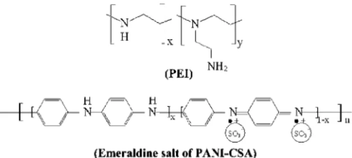
-ethyl-hexyloxy兲-1 c4-phenylene兴 共MEH-PPV兲-based polymer light-emitting diode by employing PANI-CSA as a transparent anode. Based on the concepts described above, an additional polymer electrolyte, poly共ethyleneimine兲 共PEI兲 with excess cations 共NH3+兲 that is used to compensate the anions of heavily doped PANI-CSA, is proposed for applica-tion to an organic field-effect transistor.Figure1shows the chemical structure of PANI-CSA and electrolyte PEI. The conductivity of PANI-CSA is quite high due to electronic delocalization along the backbone of the conjugated polymer. Due to the high conductivity of
PANI-CSA, it cannot be employed as the active layer of the tran-sistor without any modification. Therefore, polymer electro-lyte PEI plays an important role in modulating the conductivity of PANI-CSA via offering NH3+cations to com-pensate the SO3−anions of PANI-CSA, resulting in electronic localization along the backbone of the polymer. The degree of electronic localization along the conjugated polymer can further adjust the electric performance of the device for tran-sistor operations.
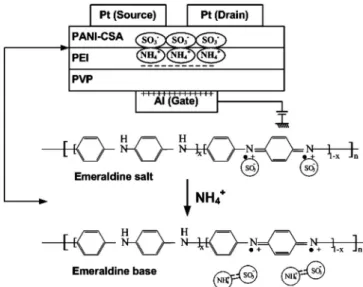
A device structure of the organic thin film transistor based on PANI-CSA with PEI is shown in Fig. 2. The Al 共60 nm thick兲 as the gate electrode was deposited on the cleaned glass substrate by sputtering. Meanwhile, the gate insulator was prepared by spin coating the PVP 共11 wt%兲/poly共melamine-co-formaldehyde兲 methylated 共4 wt%兲 in propylene glycol monomethyl ether acetate so-lution on an Al/glass gate substrate. Then it was baked on a hot plate under 170 ° C for 30 min for dielectric layer. The thickness of the cross-linked PVP was around 420 nm, giv-ing a capacitance of 5.75 nF/cm2. The PEI was spun on the PVP dielectric layer and baked on a hot plate under 100 ° C for 30 min. Next, the PANI-CSA layer was spun on the sur-face of the PEI layer and was baked on a hot plate under 100 min for 1 h. The thicknesses of PEI and PANI-CSA film are approximately 80 and 120 nm, respectively, as deter-mined by a surface profiler 共Alpha step兲. Finally, the Pt 共120 nm thick兲 source-drain electrodes were deposited on the
a兲FAX: 886-6-2080598. Electronic mail: [email protected]. FIG. 1. Chemical structures of PEI and PANI-CSA.
APPLIED PHYSICS LETTERS 92, 093508共2008兲
0003-6951/2008/92共9兲/093508/3/$23.00 92, 093508-1 © 2008 American Institute of Physics
PANI-CSA layer through a shadow mask. The channel length is 150m with the width of 1500m.
Current-voltage 共I-V兲 measurement was done using a semiconductor parameter analyzer HP4156B under atmo-spheric conditions at room temperature. The gate voltage is from 0 to 25 V with 5 V per step, while the drain voltage is from 0 to 20 V. The output characteristic of the OTFTs op-erating at different positive gate voltages is shown in Fig.3. The “doping dedoping” of conjugated polymers, with asso-ciated control of the electrical conductivity from the insula-tor to the semiconducinsula-tor, can be accomplished by chemical or electrochemical doping dedoping. Based on these con-cepts, a mechanism in which the SO3− anions in PANI-CSA was compensated by cations共NH3+兲 from PEI was sufficient to adjust PANI-CSA conductance with the applied gate bias. After PANI was doped with CSA, PANI will transform into “emeraldine salt” state and possess higher conductivity. This is because the localized electrons in the nitrogen atoms be-came delocalized and “hop” along the conjugated backbone of PANI. To adjust the conductivity of PANI, the NH3+ cat-ions were introduced from PEI into PANI to compensate the SO3− anions of PANI-CSA in order to make the electrons localized in the nitrogen atom of PANI. This results in the dedoping of PANI and makes the conversion of PANI into emeraldine base form 共Fig. 4兲. The undoped conjugated polymer contributes less free carriers than the doped one, and it possesses a low drain current at the same drain-source voltage. Therefore, the drain current decreases as the positive gate voltage increases. The decreased current for
PANI-CSA-based OTFT is concerned with the tendency of the SO3− an-ions of PANI to be compensated by the NH3+cations of PEI at the applied positive gate voltage. The stronger the electric fields applied, the more the SO3− anions were compensated by the NH3+ cations. Due to the doping-dedoping process taking place around at the interface between PEI and PANI-CSA, the SO3− anions of PANI-CSA could not be entirely compensated by the NH3+ cations. The residual SO3− anions existing in the PANI-CSA make the PANI-CSA at the “doped state” for the leakage drain-source current共Fig.3兲.
The transfer curve shows an on/off ratio共ratio between the current at a given gate voltage 0 V and that at 25 V兲 which is equal to 9.9. The effective mobility was extracted according to the following equation:
Ids=共W/2L兲Ci共Vgs− Vt兲2,
where Idsis the drain-source current, W and L are the channel width and channel length, respectively, is the field effect mobility, Ciis the capacitance per unit of area of the
insulat-ing layer, and Vgsand Vtare the gate and threshold voltage,
respectively. The mobility was calculated to be about 2.48 cm2/V s.
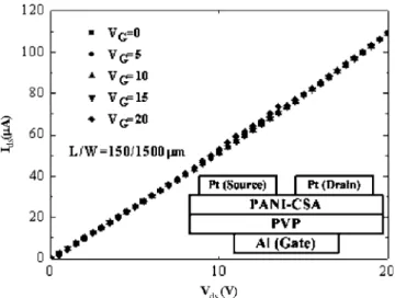
To consider the role of PEI, OTFT based on the conju-gated polymer PANI-CSA without PEI was fabricated. The current-voltage characteristics of the device based on PANI-CSA are shown in Fig.5. It is obviously shown that the I-V characteristics resemble those of a resistor instead of transis-tor behavior. Compared with the I-V characteristics of de-vices based on the PANI-CSA with and without electrolyte PEIs, the drain current of devices without PEI was larger. The lower drain current of the device based on PANI-CSA with PEI was attributed to the anions’ SO3− groups of the CSA compensated by the NH3+ cations groups of PEI. The charge carriers were localized in the nitrogen atoms. The mechanism of the conjugated polymer PANI-CSA, which is dedoped by the NH3+ cations from the polymer electrolytes PEI, is demonstrated in the above discussion. However, the drain current of device based on PANI-CSA with PEI was smaller than that without PEI while Vg was 0 V. We
sup-posed, at the interface between PANI-CSA and PEI, the SO3− anions in PANI-CSA are partly compensated by the NH3+in PEI and result in the lower conductance of PANI-CSA film. Moreover, as the positive gate voltage was increased, the FIG. 2.共Color online兲 The schematic device structure of the OTFT based on
PANI-CSA/PEI.
FIG. 3. Current-voltage characteristics of a polymer thin film transistor based on PANI-CSA/PEI.
FIG. 4. Dedoped mechanism of conjugated polymer.
093508-2 Li et al. Appl. Phys. Lett. 92, 093508共2008兲
conductance of PANI-CSA film become lower and lower due to more NH3+cations in PEI stuffed into the PANI-CSA film to compensate SO3− anions in PANI-CSA under the electric field.
In summary, an organic thin film transistor based on PANI-CSA and PEI operating in depletion mode has been demonstrated. Without the electrolyte, PEI, the device exhib-its a resistor behavior. With the insertion of the PEI layer between PVP and PANI-CSA, the device behaves as a tran-sistor working in depletion mode. This is due to the NH3+ cations of PEI stuffed into PANI-CSA to compensate the SO3− anions of PANI-CSA, thereby resulting in electron lo-calization in the PANI main chain by applying gate voltage. This work was supported in part by Chi-Mei Optoelectronics Corporation in Taiwan under Contract No. 96S034 and the National Science Council of Taiwan under contract No. NSC95-2221-E-006-428-MY3.
1H. Klauk, M. Halik, U. Zschieschang, G. Schmid, W. Radlik, and W.
Weber,J. Appl. Phys. 92, 5259共2002兲.
2Z. Shen, P. E. Burrows, V. Bulović, S. R. Forrest, and M. E. Thompson,
Science 276, 2009共1997兲.
3C. J. Drury, C. M. J. Mutsaers, C. M. Hart, M. Matters, and D. M.
de Leeuw,Appl. Phys. Lett. 73, 108共1998兲. 4M. G. Kanatzidis, Chem. Eng. News 68, 36共1990兲.
5Y. J. Lin, Y. C. Li, C. C. Yeh, S. F. Chung, L. M. Huang, T. C. Wen, and
Y. H. Wang,Appl. Phys. Lett. 89, 223518共2006兲.
6Y. Yang and A. J. Heeger,Appl. Phys. Lett. 64, 1245共1994兲.
FIG. 5. The current-voltage characteristics of a polymer thin film transistor based on PANI-CSA without PEI. The inset shows the structure of the device.
093508-3 Li et al. Appl. Phys. Lett. 92, 093508共2008兲