S. J. Peartona兲
Department of Materials Science and Engineering, University of Florida, Gainesville, Florida 32611
共Received 10 March 2005; accepted 9 August 2005; published online 27 September 2005兲 The performance of AlGaN / GaN heterostructure field-effect transistors 共HFETs兲 with either uncapped surfaces or with low-temperature共LT兲 GaN or SiO2or SiNxas gate insulators is reported. The sheet carrier concentrations of AlGaN / GaN HFETs with any of these surface insulating layers are similar to each other and in each case about 50% higher than that in an AlGaN / GaN HFET with a free surface. This result is consistent with the insulator layers providing passivation of surface states that cause the depletion of the channel layer. Due to the closer lattice match with the AlGaN surface layer, the HFET with a LT-GaN layer as the gate insulator shows the best dc and rf device performance, demonstrating that this material is an effective insulator for nitride electronic devices. © 2005 American Institute of Physics.关DOI:10.1063/1.2058173兴
INTRODUCTION
The recent progress in the development of AlGaN / GaN heterojunction field-effect transistors 共HFETs兲 for high-frequency and high-power applications has been very rapid.1–6The wide band gap and high breakdown voltage of this materials system means that AlGaN / GaN HFETs have enormous potential for uncooled operation in high-temperature environments. These devices are capable of pro-ducing very high microwave power densities共⬎12 W/mm兲, along with high breakdown voltage and low noise figures. In order to improve the performance for power, high-temperature applications, insulating gate layers are widely employed to reduce gate leakage current, increase operating voltage, and protect the device surface.5–10The use of gate insulators for compound semiconductor electronics would al-leviate many of the problems encountered in current Schottky-based devices, such as poor thermal stability. Fur-thermore, circuit design can be simplified since enhancement-mode metal-oxide-semiconductor field-effect transistors 共MOSFETs兲 can be used to form single-supply voltage control circuits for power transistors. The use of MOSFETs also allows the use of complementary devices, thus producing less power consumption and allowing for simpler circuit design. Many reports have indicated that us-ing a gate insulator on AlGaN / GaN HFETs might cause
en-hancement of the carrier density in the channel. This can be explained if the surface insulating layers reduce surface-state-related depletion of the channel layer.10 In previous works, SiO2, SiNx, AlN, Ga2O3, Sc2O3, Gd2O3, Ta2O3, and
some polymer substances have all been used as the insulating material of nitride-based HFETs.5–26 Another possibility as the gate insulator is GaN grown at low temperature 共LT-GaN兲. This is a common nucleation layer for GaN growth on sapphire but has poor crystalline quality and very high resistivity.27–31 It has quite different electrical properties from high-temperature-grown GaN layers and has been used as a stable insulating gate layer for nitride-based devices.32–36Using LT-GaN as the insulating layer of nitride-based devices has the advantage of growth within the same metal-organic chemical-vapor deposition 共MOCVD兲 system as the active layers of the HFET structure, which avoids surface contamination. In addition, the close lattice match with the nitride-based device layers reduces strain effects. In this study, LT-GaN, SiO2, and SiNxare compared as insulat-ing gate layers on AlGaN / GaN HFETs.
EXPERIMENT
Samples used in this study were all grown on c-face 共0001兲 sapphire substrates in a vertical geometry MOCVD reactor.37,38 Silane 共SiH4兲 and bicyclopentadienyl
magne-sium 共Cp2Mg兲 were used as the n-type and p-type doping
sources, respectively. A 30-nm-thick GaN nucleation layer
a兲Electronic mail: [email protected]
was first grown on top of the sapphire substrate at 560 ° C. The temperature was then raised to 1060 ° C to grow a 2-m-thick undoped GaN共n⬃3⫻1016cm−3兲 buffer layer. On
top of the buffer layer, a 50-nm-thick Mg-doped GaN layer was grown to eliminate substrate leakage current and en-hance the pinch-off characteristics.37 A 0.3-m-thick un-doped GaN was then grown at 1060 ° C to serve as the chan-nel layer. A 5-nm-thick undoped Al0.25Ga0.75N spacer and a 30-nm-thick Si-doped Al0.25Ga0.75N barrier layers 共n⬃1 ⫻1018cm−3兲 were subsequently grown as the doped regions
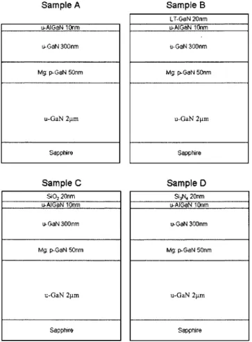
in the structure. Finally, a 20-nm-thick LT-GaN high-resistivity capping layer was grown on top of the barrier layer at 560 ° C. The sample with this structure is labeled sample B. The sample without the LT-GaN capping layer prepared under the same conditions to compare with Sample B is labeled sample A. For the gate insulator comparison, a 20-nm-thick SiO2or SiNxcap layer was grown on sample A by plasma-enhanced chemical-vapor deposition共PECVD兲. A piece of sample A with either a 20-nm-thick SiO2 or SiNx capping layer was labeled sample C or sample D, respec-tively. The schematics of samples A, B, C, and D are pro-vided in Fig. 1.
Hall-effect measurements were used to obtain the carrier concentration, using 5⫻5 mm2dimension samples with Van
der Pauw patterns. The contact areas were defined by photo-lithography. For samples B, C, and D, extra etching pro-cesses to remove the high-resistivity capping layers above the Ohmic contact areas were achieved by inductively coupled plasma 共ICP兲 etching. Ti/ Al/ Ti/ Au
共50/100/50/200 nm兲 multilayer metal was deposited by
e-beam evaporation and patterned as Ohmic contacts on the
exposed Si-doped Al0.25Ga0.75N barrier layer of each sample.
In order to study the electrical characteristics, metal-insulator-semiconductor heterojunction field-effect transis-tors 共MIS-HFETs兲 were fabricated. Mg ions were implanted into the samples for electrical isolation and also for defining active areas. After the source/drain Ohmic contact regions were defined on the active areas by photolithography, addi-FIG. 2. Scanning electron microscopy共SEM兲 micrographs of a completed device from sample B共top and center兲 and a higher magnification of the gate features共bottom兲.
tional plasma etching processes were used on samples B, C, and D to etch away the capping insulators in the Ohmic contact areas. The Ti/ Al/ Ti/ Au 共50/100/50/200 nm兲 multilayer metal was deposited onto the exposed Al0.25Ga0.75N barrier layer to serve as source/drain elec-trodes. Finally, Ni/ Au共100/100 nm兲 Schottky contacts were deposited on the gate areas to serve as the gate electrodes.
about 50% higher than the free-surface structure, sample A. This result is consistent with these insulator layers changing the electronic density of states at the Al0.25Ga0.75N barrier
layer surface and reducing the surface-related depletion of the channel layer.10 This phenomenon can be thought of as the insulator layers providing partial passivation of surface states on the AlxGa1−xN surface38,39. The LT-GaN cap layer
of sample B has a very high resistivity, larger than 1011⍀/씲. From past works, it is known that the LT-GaN is
a highly compensated material, due to the deep acceptor states originating from the high density of structural FIG. 3. Sheet carrier concentrations共ns兲 as a function of temperature for the
four samples.
defects.33–37 Therefore, this result differs from that in the conventional GaN / AlxGa1−xN / GaN heterostructure. In that
case, high-temperatugrown GaN cap layers produce a re-duction in sheet carrier concentration.40
dc electrical characteristics of the MIS-HFETs are shown in Figs. 4共a兲–4共d兲. The drain-source current/drain-source voltage 共IDS-VDS兲 characteristics were measured at room
temperature in the dark. The pinch-off characteristics in all of the devices are excellent due to the presence of the 50-nm-thick Mg-doped layer. The typical threshold voltages were around −2.5, −8, −17, and −19 V in samples A, B, C, and D, respectively. Compared with sample A, the larger threshold voltages in samples B, C, and D were attributed to the larger distance between the gate metal and undoped GaN channel layer caused by the insertion of the insulating gate layers.
Figure 5 shows the comparison of drain-source satura-tion currents 共IDSS兲 when the gate bias 共VGS兲 is at 0 V.
Samples B, C, and D have IDSS of 495, 217, and
215 mA/ mm, respectively. Those currents are higher than the IDSS of 94 mA/ mm in sample A. This result may be
attributed to the increase in effective carrier concentration in the channel in samples with insulating gate layers. From a comparison of the current ramps and the saturation currents of those samples, the different influences of the insulating cap layers become evident. Compared with a free-surface sample 共sample A兲, the structures with an insulating cap layer have a lower surface-state density that reduces the surface-related depletion effects. Moreover, the structure with a LT-GaN capping layer 共sample B兲 has a superior dc performance to the other two insulator capping layer struc-tures. This may be attributed to the better lattice match with the underlying Al0.25Ga0.75N surface layer and the absence of
contamination that might occur on moving the samples from the MOCVD reactor to the PECVD system.
In Fig. 6, the transfer characteristics from all four samples are shown. The transconductance 共gm兲 values are plotted as a function of VGS. The gmprofiles of samples B, C, and D are broader than that of sample A. This is consistent with the fact that the Schottky gate metal on the samples with insulating cap layers was further away from the current
channel layer. The broad gmprofile could in turn result in a larger gate voltage swing, improving the linearity and the dynamic range of output power. The maximum gm of samples A, B, C and D are 40, 72, 16 and 18 mS/ mm, re-spectively. The current driving ability of sample B is superior to the others. Although all of the samples with insulating cap layers produced higher drain-source saturation currents, samples C and D still could not achieve a high gm perfor-mance, which may be caused by contamination at the SiO2
-and SiNx- Al0.25Ga0.75N interfaces and the strain induced by
these dielectrics on samples C and D, respectively.
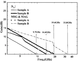
S-parameter measurements were performed for samples
A and B. In Fig. 7, the corresponding current gain 兩h21兩,
maximum stable gain 共MSG兲, and maximum available gain 共MAG兲 are given from the S-parameter measurement as a function of frequency. The fT/ fmaxvalues in samples A and B
are 9.7/ 14.4 and 19.4/ 33.8 GHz, respectively. The fT and
fmax enhancements in sample B also could be attributed to the higher transconductance, which is caused by the influ-ence of the LT-GaN capping layer.
SUMMARY AND CONCLUSIONS
In this study, the influence of LT-GaN / SiO2/ SiNx as gate insulators on AlGaN / GaN HFETs was studied. The FIG. 5. Comparison of the drain-source currents at VGS= 0 V.
high-resistivity capping layers reduce the electronic density of states at the interface with Al0.25Ga0.75N. This leads to a
reduction of surface-related depletion of the channel layer and increases the sheet carrier concentration by about 50%. AlGaN / GaN MIS-HFETs with and without gate insulators were also fabricated. Although the samples with insulating layers all exhibited higher drain-source saturation currents, samples C and D showed poorer current driving ability. This suggests that PECVD SiO2 and SiNx are not suitable gate insulators for AlGaN / GaN HFETs. By contrast, LT-GaN has the advantage of reduced surface contamination and im-proved lattice match with the AlGaN / GaN HFET active lay-ers. The Al0.25Ga0.75N HFET with a LT-GaN gate insulator
exhibited excellent dc and rf characteristics. These results suggest that LT-GaN may be a good choice as the gate insu-lator on AlGaN / GaN FETs.
ACKNOWLEDGMENTS
The authors would like to thank the National Science Council of Taiwan 共R.O.C.兲 for financially supporting this research. The work at UF is partially supported by NSF 共CTS-0301178, monitored by Dr. M. Burka and Dr. D. Senich兲, by NASA Kennedy Space Center Grant No. NAG 10-316 monitored by Mr. Daniel E. Fitch, and by NSF DMR 0400416.
1A. P. Zhang, L. B. Rowland, E. B. Kaminsky, J. B. Tucker, J. W.
Kretch-mer, A. F. Allen, J. Cook, and B. J. Edward, Electron. Lett. 39, 245 共2003兲.
2A. P. Zhang, L. B. Rowland, E. B. Kaminsky, V. Tilak, J. C. Grande, J.
Teetsov, A. Vertiatchikh, and L. F. Eastman, J. Electron. Mater. 32, 388 共2003兲.
3S. J. Pearton, J. C. Zolper, R. J. Shul, and F. Ren, J. Appl. Phys. 86, 1
共1999兲, and references therein.
DenBaars, Appl. Phys. Lett. 68, 1850共1996兲.
14S. Arulkumaran, T. Egawa, H. Ishikawa, T. Jimbo, and M. Umeno, Appl.
Phys. Lett. 73, 809共1998兲.
15F. Ren et al., Solid-State Electron. 42, 2177共1998兲.
16L. W. Tu, P. H. Tsao, K. H. Lee, I. Lo, S. J. Bai, C. C. Wu, K. Y. Hsieh,
and J. K. Sheu, Appl. Phys. Lett. 79, 4589共2001兲.
17L. W. Tu, W. C. Kuo, K. H. Lee, P. H. Tsao, C. M. Lai, A. K. Chu, and J.
K. Sheu, Appl. Phys. Lett. 77, 3788共2000兲.
18G. Simin, A. Koudymov, A. Tarakji, X. Hu, J. Yang, M. Asif Khan, M. S.
Shur, and R. Gaska, Appl. Phys. Lett. 79, 2651共2001兲.
19J. W. Johnson et al., Appl. Phys. Lett. 77, 3230共2000兲.
20B. P. Gila, J. W. Johnson, K. N. Lee, V. Krishnamoorthy, C. R. Abernathy,
F. Ren, and S. J. Pearton, ECS Proceedings Volumes 2001-1 共Electro-chemical Sociey, Pennington, NJ 2001兲, p. 71.
21M. Asif Khan, X. Hu, A. Tarakji, G. Simin, J. Yang, R. Gaska, and M. S.
Shur, Appl. Phys. Lett. 77, 1339共2001兲.
22G. Simin et al., IEEE Electron Device Lett. 22, 53共2001兲.
23T. Hashizume, E. Alekseev, D. Pavlidis, K. S. Boutros, and J. Redwing, J.
Appl. Phys. 88, 1983共2000兲.
24N.-Q. Zhang, S. Keller, G. Parish, S. Heikman, S. P. DenBaars, and U. K.
Mishra, IEEE Electron Device Lett. 21, 421共2000兲.
25B. P. Gila et al., Phys. Status Solidi A 188, 239共2001兲.
26J.-S. Lee, A. Vescan, A. Wieszt, R. Dietrich, H. Leier, and Y.-S. Kwon,
Electron. Lett. 37, 130共2001兲.
27X. H. Wu et al., Appl. Phys. Lett. 68, 1371共1996兲.
28L. Cheng, G. Zhang, D. Yu, and Z. Zhang, Appl. Phys. Lett. 70, 1408
共1997兲.
29M. S. Yi, H. H. Lee, D. J. Kim, S. J. Park, D. Y. Noh, C. C. Kim, and J.
H. Je, Appl. Phys. Lett. 75, 2187共1999兲.
30A. Estes Wickenden, D. K. Wickenden, and T. J. Kistenmacher, J. Appl.
Phys. 75, 5367共1994兲.
31D. K. Wickenden, J. A. Miragliotta, W. A. Btyden, and T. J. Kistenmacher,
J. Appl. Phys. 75, 7585共1994兲.
32J. K. Sheu et al., J. Electron. Mater. 32, 400共2003兲. 33S. J. Chang et al., IEEE Electron Device Lett. 24, 212共2003兲. 34M. L. Lee et al., Appl. Phys. Lett. 82, 2913共2003兲.
35C. J. Kao, J. K. Sheu, W. C. Lai, M. L. Lee, M. C. Chen, and G. C. Chi,
Appl. Phys. Lett. 85, 1430共2004兲.
36J. K. Sheu, Y. K. Su, G. C. Chi, M. J. Jou, C. M. Chang, C. C. Liu, and W.
C. Hung, J. Appl. Phys. 85, 1970共1999兲.
37J. K. Sheu et al., J. Vac. Sci. Technol. B 18, 729共2000兲.
38F. W. Smith, A. R. Calawa, C. L. Chen, M. J. Manfra, and L. J. Mahoney,
IEEE Electron Device Lett. 9, 77共1988兲.
39B. Luo et al., Appl. Phys. Lett. 80, 1661共2002兲. 40B. Jogai, J. Appl. Phys. 93, 1631共2003兲.
FIG. 7. Comparison of兩h21兩, MSG, and MAG measured from S parameters