台灣師範大學機電科技學系 -1-
楊 啟 榮 博士
教 授
國立台灣師範大學 機電科技學系
Department of Mechatronic Technology National Taiwan Normal University
Tel: 02-23583221 ext. 14 E-mail:[email protected]
非矽基微加工製程與應用技術 非 矽基微加工製程與應用技術
Non-Si-Based Micromachining Technology and its Applications in Microsystem Field
C. R. Yang, NTNU IMT
綱 綱 要 要
z
LIGA與LIGA-Like製程與應用技術
z
SIGA製程與應用技術
z
軟式微影製程與應用技術
z
非矽基微光學元件製作技術
台灣師範大學機電科技學系 -3-
LIGA與 LIGA 與LIGA LIGA- -Like Like製程與應用技術 製程與應用技術
C. R. Yang, NTNU IMT
LIGA技術 X-ray深光刻術
LIGA-like 技術
紫外光厚膜光阻微影 準分子雷射微加工 感應耦合電漿離子蝕刻*
電子束光刻術
切削加工 微切削加工、微鑽孔加工、微銑削加工、微輪磨加工 非切削加工 微電鍍成形、微壓模成形、微射出成形、微沖壓成形 特殊加工 微放電加工、雷射微加工、離子束微加工、電子束微加工、
超音波微加工、原子力顯微加工術 高分子微加工
技術
微雷射光合高分子成形(Microstereolithography, μ-SL) 軟式微影技術(Soft Lithography)
微接觸印刷術(Microcontact Printing, μ-CP) Micromolding in Capillaries (MIMIC) Microtransfer Molding (μ-TM) Replica Molding (REM) 其他低溫製程技
術與材料
聚對二甲苯(Parylene)、明膠(Gelatin)蛋白質、鐵氟龍(Teflon)、矽膠(Silicone) 微機械加工
精密電鑄技術 y純金屬電鑄 y合金電鑄
微微成形技術 y 塑膠微結構成形 熱壓成形、射出成形 輪壓成形、紫外線硬化法 y陶瓷微結構成形 粉末射出成形、 帶板鑄造
非 矽 基 微 加 工
MEMS領域中微製造技術分類表 MEMS 領域中微製造技術分類表
註:感應耦合電漿離子蝕刻技術通常歸類為非等向性高深寬比矽基蝕刻技術。
台灣師範大學機電科技學系 -5-
2. 顯影
4. 金屬模仁
6. 脫模
Mould cavity Resist structure
Plastic structure
5.模造 3. 電鑄 1. 光刻
Plastic (moulding compound)
Metal Resist structure
Electrical conductive base plate Base plate Absorber structure Maskmembrane
Resist
Source: Institut für Mikrotechnik Mainz (IMM), Germany
Li
thographie:光刻G
alvanoformung:電鑄A
bformung:模造LIGA製程: LIGA 製程:
高深寬比高深寬比((high aspect high aspect ratio)
ratio)的微結構的微結構
MCNC
C. R. Yang, NTNU IMT
LIGA製程技術 微電鑄技術
複合製程技術 微成型技術
Deep lithography
電鍍液配方
合金微電鍍技術 陶瓷複合
電鍍技術 純金屬 電鍍技術
光罩製造技術 光阻塗佈技術
Alignment技術
光阻材料技術
反應性微射出成型
塑膠微射出成型
陶瓷微射出成型 微陶瓷結構燒結技術 熱壓微成型
陶瓷精密脫蠟技術
Bonding技術
製程設計技術 Alignment技術
LIGA製程技術的技術關聯圖 LIGA 製程技術的技術關聯圖
台灣師範大學機電科技學系 -7-
犧牲層LIGA (S 犧牲層 LIGA (S- -LIGA) LIGA) 技術的應用範圍 技術的應用範圍
z微感測器的懸浮結構
z可控制流量進出的微閥門
z各型微致動器的移動或轉動結構等…...
Micromotor Micropump
Acceleration microsensor
C. R. Yang, NTNU IMT
Key Features of X
Key Features of X- -ray LIGA Microstructures ray LIGA Microstructures
z
Realization of arbitrary shape
z
Extreme structure height (>mm)
z
Extreme aspect ratio (>100)
z
Minimum lateral dimensions 0.5±0.1μm
z
Surface roughness 0.03-0.05 μm
z
Vertical & smooth sidewalls
z
Wide variety of materials
z
Successful in mass fabrication
IMT and IMM, Germany
台灣師範大學機電科技學系 -9-
( a ) 微齒輪組 ( b ) 微鏡片 ( c ) 整合光學分光器 ( d )近場光學探針 ( e ) 微熱交換器
( f ) 微組合 ( h ) 微幫浦 ( g ) 微反應器 ( i ) 光纖固定器 ( j ) 微馬達
( k ) 光纖開關 (l) 微小直升機 IMM微系統研究中心
IMM微系統研究中心所開發的產品 IMM 微系統研究中心所開發的產品
Source: http://www.imm-mainz.de
C. R. Yang, NTNU IMT
IMT微系統研究中心所開發的產品 IMT 微系統研究中心所開發的產品
Source: http://www.fzk.de/imt/eimt
台灣師範大學機電科技學系 -11-
LIGA
LIGA 製程 製程 vs. 類 vs. 類LIGA LIGA 製程 製程
光刻源的差異 LIGA 製程: 同步輻射X光
類LIGA 製程: 低成本替代性光源
z加工深度數mm、次微米級精度、深寬比>100
z同步輻射光源為一龐大且昂貴的設備
zX-ray 光罩製作複雜且成本高
z加工深度≦ 1mm、微米級精度、深寬比≦50
z紫外光–厚膜光阻微影製程
z準分子雷射
z反應性離子蝕刻
C. R. Yang, NTNU IMT
Synchrotron Radiation Research Center (for LIGA process) Synchrotron Radiation Research Center (for LIGA process)
JAPAN SPring-8
USA APS FRANCE ESRF
ICP-RIE System Excimer Laser System UV mask aligner
Low- Low -cost Exposure System (for LIGA cost Exposure System (for LIGA- -like process) like process)
Instrument Technology Research Center, ITRC
台灣師範大學機電科技學系 -13-
Source: http://daytona.ca.sandia.gov/LIGA/mask.html ( Sandia National Laboratory, USA )
Photomask
Photomask of UV Lithography of UV Lithography
(a) CAD Layout (b) Chrome Mask
C. R. Yang, NTNU IMT
Comparison of a low energy x-ray mask (left) and a high energy x-ray mask (right) both designed and created at Wisconsin.
4μm Gold on a 1μm SiN membrane
50μm Gold on a 400μm Si substrate
Photomask
Photomask of X- of X -ray Lithography ray Lithography
台灣師範大學機電科技學系 -15-
具厚膜光阻及電鑄起始層的試片製備方法 具厚膜光阻及電鑄起始層的試片製備方法
Substrate with seed layer Special Special Photoresist Photoresist
Spin coater
Vacuum
Spin coating process
Dry film Dry film
Substrate with seed layer
Laminating process
Glass plate Substrate with seed layer
Pressing machine
Solvent bonding process Solvent layer Solvent layer Polymer film Polymer film
Spacer
Polymerized resist Polymerized resist
Casting machine
Casting process Glass plate Substrate with seed layer
Pretreatment glass plate Separation foil
Polymer film Polymer film Separation foil
C. R. Yang, NTNU IMT
(1) 塗佈光阻
聚合物 基材
(2) 光蝕刻
雷射光
電鑄起始層
(3) 金屬濺鍍
金屬
(4) 電鑄
金屬模
聚合物 (5) 研磨修整
(6) 剝離
(7) 熱壓印成形
(8) 脫模
substrate seed layer
photoresist nickel
光學元件之LIGA製程示意圖
母模幾何形狀與電鑄起始層位 置對電鑄沈積層的影響示意圖
台灣師範大學機電科技學系 -17-
Schematic of a X-ray mask/substrate scanner
Source: http://daytona.ca.sandia.gov/LIGA/mask3.html
X-Ray Scanner DEX 02
JENOPTIK Mikrotechnik GmbH
X- X -ray Deep Lithography Scanner ray Deep Lithography Scanner
C. R. Yang, NTNU IMT
(c) LIGA microstructure with inclined sidewalls
Fabrication of microstructure with inclined sidewalls
(b) development (a) SR exposure
SR
mask resist
substrate
resist structure
台灣師範大學機電科技學系 -19-
Fabrication of
Fabrication of nonplanar nonplanar microstructure microstructure
X-ray lathe
Microstructure on the cylindrical substrate
helical structure mask SR
blank substrate
mask SR
mask SR
Source: A. D. Feinerman et al., J. Microelectromechanical Systems, 5(4) (1996) 250-225
C. R. Yang, NTNU IMT
Fabrication Techniques of Novel Microstructures Fabrication Techniques of Novel Microstructures
using
using Excimer Excimer Laser Ablation Laser Ablation
以不同雷射,加工 Polyimide 的結果比較:
(a) Nd-YAG laser, (b) CO2 laser, (c) Excimer laser F2(157 nm)、ArF (193 nm)、KrF (248 nm)、
XeCl (308 nm)、XeF (351nm)
台灣師範大學機電科技學系 -21-
Optimum laser Materials
XeCl
308 nm KrF
248 nm ArF
193 nm F2
157 nm
Polymer PEEK, PEI, PET, PI PA, PES, PC, PUR, PPS, Polyparaxylylene
Polyacetylene, PE, PMMA, PS, PVC, PVDC,
PVOH, PVDF, Silicone rubber, Nitrocellulose
PTFE (Teflon)
Composites of fibers in epoxy
Glass fiber, Carbon fiber, Aramid Ceramics Alumina, LiTaO3,
SiC, Si3N4, ZrO2
Si3N4(gas pressure sintered or reaction
bonded), PZT
SiC (toughened)
Crystals and glasses
Fused silica, SiO2, Silicon, Borosilicate glass, Yttrium aluminium garnet (YGA)
GaAs, quartz, fused silica, sapphire, silicon
Metal film Aluminium, Copper
Biological tissue
Artery wall, Bile duct, Carcinoma tumour, Prostate
tissue
Cornea
Teeth Enamel, Dentine
Optimum
Optimum Excimer Excimer Laser for Various Materials Laser for Various Materials
R. C. Crafer and P. J. Oakley, Laser processing in manufacturing, Chapman & Hall, New York, 1993
C. R. Yang, NTNU IMT
台灣師範大學機電科技學系 -23-
Excimer
Excimer Laser Micromachining Laser Micromachining
Laser LIGA technology Laser LIGA technology
Fresnel structure ablated into dry filmwith 50 μm thick
Nickelelectroplated metallic microstructure
C. R. Yang, NTNU IMT
以控制工件平台運動狀態之方式進行雷射加工
以控制工件平台運動狀態之方式進行雷射加工
台灣師範大學機電科技學系 -25-
Excimer
Excimer Laser Laser Micromachining: Mask Dragging Micromachining: Mask Dragging
以光罩拖拉(移動工件平台)技巧進行雷射加工的方式
shaped mask
可快速製作不同幾何斷面之微流道
C. R. Yang, NTNU IMT
A B C D E F
A: Fresnel 波帶片 B: 平面化二元式Fresnel微透鏡
C: 兩階二元式Fresnel微透鏡 D: 四階二元式Fresnel微透鏡
E: 鋸齒狀Fresnel微透鏡 F: 傳統透鏡
不同之 不同之 Fresnel透鏡與傳統透鏡之比較圖 Fresnel 透鏡與傳統透鏡之比較圖
台灣師範大學機電科技學系 -27-
SU-8光阻微透鏡陣列 光強度分布圖
氦氖雷射 CCD
物鏡
物鏡 折射式微透鏡
陣列 針孔
透鏡 光圈
三維移動平台
光束品質 分析器
光學檢測設備架構圖
準分子雷射應用於微透鏡陣列之製作技術 準分子雷射應用於微透鏡陣列之製作技術
光罩圖案示意圖
C. R. Yang, NTNU IMT
Mask
Workpiece Stage
Fresnel Lens
以Mask Dragging 以 Mask Dragging 的方式製作微鏡片 的方式製作微鏡片
(b) Groove pattern of the kinoform cylindrical lens (a) Mask used to make cylinderical lens
Dark: 透光 Clear:不透光
台灣師範大學機電科技學系 -29-
背光模組光反射元件的製作 背光模組光反射元件的製作
C. R. Yang, NTNU IMT
http://www.exitech.co.uk/
台灣師範大學機電科技學系 -31-
準分子雷射單光罩多層階加工技術 準分子雷射單光罩多層階加工技術
光罩圖案
雷射 聚焦成像
加工圖案重疊
(光罩移動)
(工件固定)
光罩圖案
12 3
2 1
2 3
3 3
3 八階光罩組合
準分子雷射微透鏡加工技術
C. R. Yang, NTNU IMT
準分子雷射微加工 準分子雷射微加工
微光學繞射元件製作與檢測
微光學元件檢測系統
像素5 μm四階全像片 “HELLO” 影像輸出 焦平面光強度 十六階微透鏡陣列
孔徑250 μm、焦距15 mm
表面檢測 光學檢測 準分子雷射LIGA製程
台灣師範大學機電科技學系 -33-
Applications of Ultrathick Photoresist for Microstructure Fabrication
光罩對準UV曝光系統 特殊光阻塗佈機
●Low-Cost LIGA製程的發展因素:
(Poor-Man LIGA Technology)
z厚膜光阻材料的開發
z特殊光阻塗佈機的發展
zUV曝光設備的改良
● 厚膜光阻材料
AZ4000 series, Hoechst (Germany)
ma-P 100, ma-N 400, Micro resist technology (Germany)
PMER P-LA 900, tok (Japan)
Probimide, Olin microelectronic materials (Japan)
THB-611P, THB-430N, JSR (Japan)
SU-8, Microlithography chemical corporation (USA)
C. R. Yang, NTNU IMT
SU- SU -8 8厚膜光阻 厚膜光阻 UV UV -LIGA - LIGA製程 製程
光阻微結構 vs. 螞蟻
國科會精密儀器發展中心 (PIDC)
電鑄鎳金屬結構
台灣師範大學機電科技學系 -35-
Preparing
Preparing Photoresist Photoresist Reflow Lens Pattern Reflow Lens Pattern
H. Toshiyoshi
C. R. Yang, NTNU IMT
Lens Shape (Sag) After
Lens Shape (Sag) After Photoresist Photoresist Reflow Reflow
as a function of initial resist thickness
as a function of initial resist thickness台灣師範大學機電科技學系 -37-
Transferring
Transferring Photoresist Photoresist Pattern into Silicon Pattern into Silicon
C. R. Yang, NTNU IMT
(b) 曝光顯影
(c) 鍍Cr/Au
(d) Lift-off
(e) 正光阻 (犧牲層)
(f) 曝光顯影
(g) 鍍Ti/Cu
(i) 曝光顯影
(j) 電鑄Ni (h) 負光阻
(k) 去除光阻結構釋放 (a) 上正光阻
犧牲層厚膜光阻製程技術
犧牲層厚膜光阻製程技術
台灣師範大學機電科技學系 -39-
厚膜光阻與犧牲層技術於微元件的開發應用 厚膜光阻與犧牲層技術於微元件的開發應用
( a ) 微繼電器 ( b ) ( a )圖之局部放大圖
( c ) 微致動器 ( d ) ( c )圖之局部放大圖
C. R. Yang, NTNU IMT
Movable Microstructure fabricated by Single Mask Movable Microstructure fabricated by Single Mask
Lithography & Dry Releasing Techniques Lithography & Dry Releasing Techniques
Micro-relay fabrication process
(a) SU-8 resist lithography
(b) Dry etching
(c) Metal Sputtered
Micro-relay, PIDC
台灣師範大學機電科技學系 -41-
0 30 60 90 120
1 2 3
Voltage
數列1
側位移量25 側位移量 25μ μm m不同彈簧結構下所需驅動電壓 不同彈簧結構下所需驅動電壓
Micro-relay, PIDC
C. R. Yang, NTNU IMT
Application of ICP RIE
Application of ICP RIE- -LIGA Process LIGA Process
Fabrication of Silicon Fuel
Fabrication of Silicon Fuel AtomiserAtomiser
Si mold
Ni atomizer
1. Grow oxide and pattern
2. Spin on thick resist and pattern
3. First 275 μm deep DRIE etch
4. Remove oxide and second DRIE etch for an additional 125 μm
6. Polish excess and release 5. Deposit 400 μm of Ni
Fabrication of Silicon Fuel
Fabrication of Silicon Fuel AtomiserAtomiser
台灣師範大學機電科技學系 -43-
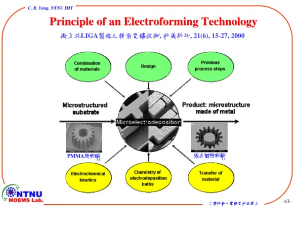
Principle of an Electroforming Technology Principle of an Electroforming Technology
PMMA微齒輪 鎳金屬微齒輪
微系統LIGA製程之精密電鑄技術, 科儀新知, 21(6), 15-27, 2000
C. R. Yang, NTNU IMT
E-beam mask
Intermediate mask
Working mask
Resist structure
Mold insert
Lots of Plastic/ceramic
products
Electro- forming
Plastic molding
Au
Au Metal
products
Lots of Metal products
Cu, Au Ni, Ni-Fe
Ni, Ni-Fe Ni-Co, Ni-W Alloys, Composites
Cu, Au, Ni, Ni-Fe, Ni-Co, Ni-W, Alloys, Composites Electro-
forming
Lithography, Development
Electro-
forming Electro-
forming
Illustration of electroforming role within LIGA process
●X-ray mask ●Metallic microstructures ●Mold insert
台灣師範大學機電科技學系 -45-
Ni Metal microstructures, mold inserts Au Absorber material for X-ray mask
Material for intermediate layers
Cu Microstructures, Material for intermediate layers Ni-Fe High magnetic and corrosion resistance property
Invar (64% Fe: 36% Ni) — low thermal expansion property Thermal coefficient of expansion (TCE):
Ni:13.4×10⁻⁶/K Cu: 16.5×10⁻⁶/K Silicon: 2.6×10⁻⁶/K Invar: 2.0×10⁻⁶/K
Permalloy (21% Fe: 79% Ni) — high magnetic property Saturation magnetization:
Nickel:6K Gauss Permalloy: 10K Gauss
Ni-Co High strength property for punch mold Ni-Mn High hardness property for punch mold
Ni-W High temperature resistance property
Characteristics and Application of Electroformed Metals Characteristics and Application of Electroformed Metals
C. R. Yang, NTNU IMT
Schematic of an electrochemical cell
Power supply
Cathode Anode
e- e-
Ni → Ni2+ → Ni 2e- 2e-
2H2O + 2e-→ H2+ 2OH-
↑
H2 ↑
H2
↑ H2
↑ H2
Ni deposition H2evolution Ni dissolution
台灣師範大學機電科技學系 -47-
Electrolyte Laminar flow
Microstructured polymer layer
Conducting substrate as cathode
mass transport mainly by convection mass transport mainly by diffusion
Mechanisms of mass transport to recessed microelectrodes of different lateral dimensions during electroforming
C. R. Yang, NTNU IMT
高分子微結構製作 試片前處理 參數控制
高分子層與電鑄基板結合 RIE 去除 純水清洗 電流密度 陰極擺動速率 電鑄種子層長成 殘餘光阻 酸洗活化 表面張力 鍍液組成
結構分布均勻 脫脂 銀鏡反應 遮板使用 陰陽極效率
結構尺寸一致 無電鍍 離型劑使用 輔助電極 電流波形 時間、溫度 pH 值
電鑄技術影響參數
流場設計 攪拌方式 金屬濃度 複合電鑄濃度 成份比例 溫度控制 循環過濾 合金電鑄濃度 雜質分析與過濾 機械性質
陰極擺動 電極設計 安定劑 活性碳處理 物理性質
液位控制 藥液自動 光澤劑、硼酸 弱電解處理 表面特性 電流供應 分析添加 平坦劑、溼潤劑 應力降低劑 複製精確度
電鑄槽設計 鍍液成份管理 電鑄品檢測分析
LIGA製程之電鑄品質影響參數與條件 LIGA 製程之電鑄品質影響參數與條件
DC, pulsed, periodic reverse current
台灣師範大學機電科技學系 -49- (1) 塗佈光阻
聚合物 基材
(2) 光蝕刻
雷射光
電鑄起始層
(3) 金屬濺鍍
金屬
(4) 電鑄
金屬模
聚合物 (5) 研磨修整
(6) 剝離
(7) 熱壓印成形
(8) 脫模
substrate seed layer
photoresist nickel
光學元件之LIGA製程示意圖
母模幾何形狀與電鑄起始層位 置對電鑄沈積層的影響示意圖
C. R. Yang, NTNU IMT
氣泡所造成的缺陷 後處理所造成的缺陷
一般常見之電鑄缺陷與解決之道 一般常見之電鑄缺陷與解決之道
內應力導致電鑄層嚴重變形 內應力已獲得控制之鑄層
台灣師範大學機電科技學系 -51- 電源
供應器
陽極 遮蔽
陰極
電源 供應器
電流密度分布
( a ) ( b )
(a) (a) 陰陽極間電流密度分布;陰陽極間電流密度分布;(b) (b) 遮蔽使陰極表面電流密度均勻化示意圖遮蔽使陰極表面電流密度均勻化示意圖
電鑄層厚度控制方法
電鑄層厚度控制方法- -增加遮蔽層 增加遮蔽層
C. R. Yang, NTNU IMT
電鑄層厚度控制方法
電鑄層厚度控制方法- -外圍虛電鑄區 外圍虛電鑄區
無增加虛電鑄區
增加虛電鑄區
台灣師範大學機電科技學系 -53-
電流密度分布
電流密度分布對薄光阻結構電鑄厚度影響示意圖 電流密度分布對薄光阻結構電鑄厚度影響示意圖
電鑄金屬 電鑄起始層
光阻
C. R. Yang, NTNU IMT
a
電流密度分布
a/b=1/4
a/b=6/1 b
電鑄金屬 電鑄起始層
光阻
overplating
Plating stopped at ~2/3 of the total depth
不同深寬比對電鑄輪廓曲線影響示意圖
台灣師範大學機電科技學系 -55-
電鑄金屬 電鑄起始層 光阻
避免鑄層沈積厚度差異過大之製程示意
避免鑄層沈積厚度差異過大之製程示意(a) (a) 改良前;改良前;(b) 改良後(b) 改良後
( a ) ( b )
C. R. Yang, NTNU IMT
精密電鑄技術 精密電鑄技術
金屬模仁製作
精密電鑄設備, NTNU MOEMS Lab.
微齒輪
鎳電鑄結構 高分子光刻圖案
Fresnel圖案 (深寬比25)
四階全像片 像素5 μm
z光學元件:線寬≦1 μm 、深寬比3 z高深寬比微結構:線寬10 μm、深寬比25 技術
能量
台灣師範大學機電科技學系 -57-
光電業
導線架 微過濾器
微閥 微感測器
微致動器
CD DVD
民生工業
票券印製 珠寶飾品 信用卡 識別證 特殊網罩
機械工業
微機械零件 精密模具
精密儀器 耐磨零件
伸縮囊管
通訊工業
導波管
光纖耦合器
非球面反射鏡 抬頭顯示器 全像片 光學鏡片
半導體工業
精密電鑄技術
精密電鑄技術的應用領域 精密電鑄技術的應用領域
(資料來源:中科院)
C. R. Yang, NTNU IMT
塑膠微模造成型技術 塑膠微模造成型技術
z
熱印壓模法
(Hot embossing) z微射出成型
(Injection molding)
反應式射出成型技術
(Reactive Injection Molding, RIM)
熱鑄式射出成型技術
(Thermal Injection Molding, TIM)大量批次(batch)生產、降低成本、滿足工業市場需求
台灣師範大學機電科技學系 -59-
反應式射出成型示意圖
z鑄材成份在射出前才混合
z常用於熱固型樹脂
z成份必須以精準重量比例混合
z低黏度液體以低壓(約10bar)射入模仁內
缺點:
z必須使用真空模去除氣泡
z高分子聚合反應性強,具爆炸性
z模內壁之平滑要求高,否則脫模困難
C. R. Yang, NTNU IMT
熱鑄式射出成型示意圖
z鑄材加熱後才射入模仁內
z適用材料範圍廣:
熱塑性塑料
熱固性樹脂
橡膠
熱鑄射出成型之步驟:
1. 加熱塑化 2. 高壓射出注模 3. 冷卻脫模
台灣師範大學機電科技學系 -61-
Principle of Hot Embossing Process
Heating and cooling for temperature control
C. R. Yang, NTNU IMT
Design
CNC-μMachining μEDM
Si-processes Wet etch Dry etch DEEMO
High resolution techniques LIGA LIGA-like
Vacuum heating of substrate and tool
above Tg
Contact force typ.
several kN
Cooling of tool and substrate
below Tg Demolding
Bonding of cover lid Mold insert fabrication
Embossing process
Hot Embossing Process Schematics Hot Embossing Process Schematics
Quality control Trimming
DEEMO: Dry Etching, Electroplating, Moulding
台灣師範大學機電科技學系 -63-
IR- IR -Spectrometer Spectrometer produced by injection molding produced by injection molding
Self-focusing blazed reflective grating
•spectral range: 3.0 μm - 4.3 μm
•dispersion: 0.23 μm/mm
•spectral resolution: 0.07 μm
Cover plate coated with gold
Linear focal line ready to attach to detector array
mirror Gold coating
Molded polymer substrate
Entrance (free-space optics or fiber optics)
C. R. Yang, NTNU IMT
Hollow waveguide
Gas Miniature tungsten lamp
PbSe detector
Self focusing reflection grating
Gas microsensor with an integrated IR-spectrometer
Source: http://www.microparts.de/01OPTICIR.htm Characteristics
zEconomical in high volumes because of injection molding techniques
zCompact and robust
zNo moving parts
zHigh measuring stability through dual beam principle
台灣師範大學機電科技學系 -65-
Principle of the VIS
Principle of the VIS- -Spectrometer Spectrometer
Source: http://www.microparts.de/01OPTICVIS.htm Light input λ1….λx
through optical fiber
Light output via
45oreflecting edge Diode array
Self focusing reflection grating (d=0.2 μm, g=2 μ m)
λ2λ1 Characteristics
zMolded construction allows for cost effective volume pricing
zSmall dimensions, lightweight
zExcellent thermal stability
zLong-term stability
zFlexible operation
zRobust monolithic construction
zNo moving parts
C. R. Yang, NTNU IMT
LIGA技術的未來發展方向 LIGA 技術的未來發展方向
z
更高深寬比微結構的開發:
曝光設備、高敏感光阻z 3D微結構的開發:曲面、複雜微結構
z
複合製程的開發:
整合IC製程與微機械加工、製程設計規劃 z新合金材料電鑄技術的開發:
金屬基陶瓷複合材z
陶瓷材料成型及燒結技術的開發:
壓電、磁致伸縮陶瓷 z新型微系統產品的開發與應用
台灣師範大學機電科技學系 -67-
SIGA製程與應用技術 SIGA 製程與應用技術
C. R. Yang, NTNU IMT
SiO2 Si
Si (a) 熱氧化沉積SiO2
(b) 微影及用BOE蝕刻SiO2
(c) 以最佳蝕刻參數蝕刻
Si SiOPR2
SiO2
Si
(d) 使用BOE去除SiO2
Si Cr/Cu
(e) 蒸鍍電鑄起始層Cr/Cu
Si Cr/Cu
Ni
(f) 微鎳電鑄
(g) 脫模
In German: In English:
Silizum-mikrostrukyur Silicon-microstructuring Galvanoformum Electroforming
Abformung Molding
SIGA SI GA製程 製程: :
台灣師範大學機電科技學系 -69-
矽模仁 二次電鑄鎳模仁 PMMA壓模成形
微結構充填不足
微結構收縮變形 一次電鑄鎳模仁
C. R. Yang, NTNU IMT
Lenses
Gratings Waveguides Holograms
成形方法:
1. Lithography +RIE etching 2. Photoresist reflow
3. Direct writing of e-beam or laser 4. Shaped light beam method 5. Grey tone mask technique
Grey tone mask technique Shaped light beam method
Direct writing of e-beam
SIGA製程應用技術 SIGA 製程應用技術 ( 1 ) ( 1 )
台灣師範大學機電科技學系 -71-
Lens profile in resist on glass or silicon
Ion etching
Lens profile etched into glass or silicon
Ni stamper
glass UV-curable polymer
UV exposure
Ni stamper
Substrate
Polymer film
C. R. Yang, NTNU IMT
軟式微影製程與應用技術
軟式微影製程與應用技術
台灣師範大學機電科技學系 -73-
Soft Lithography Soft Lithography
軟式微影製程主要是利用一種透明的彈性高分子聚合材料二甲基矽氧 烷(polydimethylsiloxane, PDMS),作為翻模用的彈性印章(stamp),利 用印章圖形轉移的方式,並搭配不同的後處理(如蝕刻、灌模等),來 完成各種不同的微結構。
製程尺寸的範圍從30 nm 到100 nm,應用的範圍包括光學導線、感測 器、致動器、微型幫浦、生醫晶片、微流結構與奈米表面處理等。
SU-8 master structure PDMS replica of SU-8 master structure Hong et al., Columbia University
C. R. Yang, NTNU IMT
n=~60
n=~10
台灣師範大學機電科技學系 -75-
Advantage and Disadvantage of PDMS Advantage and Disadvantage of PDMS
zz
Advantage : Advantage :
(1) Favorable mechanical properties (1) Favorable mechanical properties
(such as extreme
(such as extreme flexibility and stability
flexibility and stability)) (2) Good optical properties (2)
Good optical properties(transparent)
(transparent)(3) High biocompatibility
(3) High biocompatibility (4) Peel off the PDMS easily (4) Peel off the PDMS easily (5) Low costs
(5) Low costs
zz
Disadvantage : Disadvantage :
(1) Use soft lithography techniques to fabricate (1) Use soft lithography techniques to fabricate (2) The PDMS is poisoned easily.
(2) The PDMS is poisoned easily.
C. R. Yang, NTNU IMT
毛細管微成形
毛細管微成形( (micromolding micromolding in capillaries, MIMIC) in capillaries, MIMIC)
台灣師範大學機電科技學系 -77-
Schueller et al., Sensors and Actuators A72 (1999) 125–139
Preparation of a glassy carbon microstructure with a triangular diffraction grating embossed on its surface
C. R. Yang, NTNU IMT
Preparation of a glassy carbon microstructure with a
square diffraction grating surface relief
台灣師範大學機電科技學系 -79-
Variable
Variable- -focusing focusing microlens microlens with with microfluidic microfluidic chip chip
J. Chen et al., J. Micromech. Microeng. 14 (2004) 675–680
C. R. Yang, NTNU IMT
Microfluidic
Microfluidic Chip Fabrication Chip Fabrication
J. Chen et al., J. Micromech. Microeng. 14 (2004) 675–680
台灣師範大學機電科技學系 -81-
Polymer
Polymer- -based variable focal based variable focal length
length microlens microlens system system
M. Agarwal et al., J. Micromech. Microeng. 14 (2004) 1665–1673
C. R. Yang, NTNU IMT
Series of images taken at different volumes of fluid by actuating the variable focal length lens as: (a) DCX lens, (b) DCV lens
M. Agarwal et al., J.
Micromech. Microeng. 14 (2004) 1665–1673
台灣師範大學機電科技學系 -83-
Camou et al., University of Tokyo
On the left :classic experimental set-up to perform fluorescent spectroscopy with a microscope integrating the light source, filters and lenses and on the right :example of a lab-on-a-chip device with an integrated detection system.
C. R. Yang, NTNU IMT
Towards the on
Towards the on- -chip fluorescence spectroscopy using optical chip fluorescence spectroscopy using optical fibers and PDMS material
fibers and PDMS material
Camou et al., University of Tokyo
台灣師範大學機電科技學系 -85-
Main steps to fabricate a PDMS layer from SU-8 mold, with a design that integrates a 2-D optical lens
Camou et al., University of Tokyo
C. R. Yang, NTNU IMT
Effect of the PDMS lens on the fluorescent light emission from the dye
台灣師範大學機電科技學系 -87-
非矽基微光學元件製作技術 非矽基微光學元件製作技術
C. R. Yang, NTNU IMT
Thermal impressing for the fabrication of microprism arrays
PMMA Oblique illumination
Beam splitters
Retroreflectors
Microprism
Microprism fabrication by the LIGA technique fabrication by the LIGA technique
Source: H. Peter Herzig, Micro-optics, Taylor & Francis (1997)
台灣師範大學機電科技學系 -89-
Planar integrated free
Planar integrated free- -space optics space optics
Optical pickup unit for data storage applications(Shiono and Ogawa)
C. R. Yang, NTNU IMT
Spherical lens
fiber fiber
Single-mode fibres adjusted to a ball lens Schematic of a microoptical switch with
single-mode fibres
Movable mirror and fibre grooves mirror
LIGA Process for Optical Switch
LIGA Process for Optical Switch
台灣師範大學機電科技學系 -91-
應用X 應用 X- -ray LIGA ray LIGA製程開發之光學陣列開關 製程開發之光學陣列開關
J. Mohr, A. Last, and U. Wallrabe, 8th Microoptics Conference, Osaka, Japan, (2001).
C. R. Yang, NTNU IMT
微型流式細胞
微型流式細胞 /顆粒計數與分類感測器 / 顆粒計數與分類感測器 之研發及其應用
之研發及其應用
李國賓等人, 科儀新知第24卷第4期, 92年, 15-24
台灣師範大學機電科技學系 -93-
微流體細胞計數器 微流體細胞計數器
z樣品由中間管道注入
z兩側則注入邊鞘流
z適當的操縱邊鞘流速,使中間流達到預期的寬度 (邊鞘流流速愈快,集中效果愈佳)
流式細胞/顆粒計數及分類感測器的操作原理則是利用水力所引發的流體聚焦效 應(hydrodynamic focusing effect) 而進行細胞計數及分類,其基本結構由三條 平行管道、噴嘴與集中流管道組成。
李國賓等人, 科儀新知第24卷第4期, 92年, 15-24
C. R. Yang, NTNU IMT
Pictures of a pre-focused 1 × 7 flow switch, fabricated on a quartz template (a) and then imprinted on PMMA substrates (b) using micromachining techniques and hot embossing
( a )
( b )
Lithography
Developing
Cr etching
PR stripping
Quartz etching (BOE 6:1) Quartz
UV
PR Cr film Photomask
台灣師範大學機電科技學系 -95-
微流體聚焦現象 微流體聚焦現象
⎟⎟
⎠
⎞
⎜⎜
⎝
⎛ + + +
=
2 3 2 3 3 2 2
1 2 1 5 1 . 1
2
D D v v D
D v v
aD d
ρ ρ ρ
ρ
理論公式
d、D1、D2、D3 為細胞流集中寬度和1-3入口微管道寬度 v1、 v2、 v3 為流體入口微流管道之流速
ρa、ρ1、ρ2、ρ3 為出口流體和入口微管道1-3之流體密度
李國賓等人, 科儀新知第24卷第4期, 92年, 15-24
C. R. Yang, NTNU IMT
Port B: and
Port A: and
流量比 流量比 (flow- (flow -rate rate- -ratio) ratio)控制流向法 控制流向法
李國賓等人, 科儀新知第24卷第4期, 92年, 15-24
台灣師範大學機電科技學系 -97-
流向導引部分:利用兩側邊鞘流不同的速度控制流向。
李國賓等人, 科儀新知第24卷第4期, 92年, 15-24
C. R. Yang, NTNU IMT
z(a)圖下方為無微粒子時的訊號。
z(a)圖上方為通過微粒子時的訊號
,其中每一峰值代表有一微粒子 通過。
計數器不僅可計數,還可分辨不 同粒子的大小。
( a )