GaN Schottky barrier photodetectors with SiN / GaN nucleation layer
Y. D. Jhou, S. J. Chang,a兲 Y. K. Su, and Y. Y. Lee
Institute of Microelectronics, National Cheng Kung University, Tainan 701, Taiwan;
Department of Electrical Engineering, National Cheng Kung University, Tainan 701, Taiwan; Advanced Optoelectronic Technology Center, National Cheng Kung University, Tainan 701, Taiwan; and
Center for Micro/Nano Science and Technology, National Cheng Kung University, Tainan 701, Taiwan C. H. Liu
Institute of Nanotechnology and Microsystems Engineering, National Cheng Kung University, Tainan 701, Taiwan
H. C. Lee
Institute of Electro-Optical Science and Engineering, National Cheng Kung University, Tainan 701, Taiwan 共Received 10 June 2007; accepted 15 August 2007; published online 4 September 2007兲
GaN Schottky barrier photodetectors with SiN / GaN nucleation layer were fabricated. It was found that leakage current was much smaller and much less bias dependent for the photodetector with SiN / GaN nucleation layer, as compared to the photodetector with conventional low-temperature GaN nucleation layer. It was also found that effective Schottky barrier height increased from 1.27 to 1.53 eV with the insertion of the SiN layer. Furthermore, it was found that the authors can effectively suppress internal gain of the detector and enhance ultraviolet to visible rejection ratio by using the SiN / GaN nucleation layer. © 2007 American Institute of Physics.
关DOI:10.1063/1.2779854兴
GaN has become a useful material for blue/green light emitting diodes1,2 共LEDs兲 and ultraviolet 共UV兲 photodetectors.3,4 To date, various types of GaN UV photo-detectors have been demonstrated.5–8Compared with bipolar photodetectors, the fabrication process of Schottky barrier photodetectors 共SBPDs兲 is simpler. The response speed of SBPD is also fast. However, leakage current in SBPD is higher. It is known that leakage current depends strongly on the quality of the epitaxial layers. For GaN prepared on sap-phire, dislocation density is high due to the large mismatches in lattice constant and thermal expansion constant. Thus, leakage current in GaN-based SBPD is high in general. Con-ventional method to overcome this problem is to deposit a thin low-temperature共LT兲 GaN nucleation layer prior to ep-itaxial growth. To further reduce dislocation density, tech-niques such as epitaxial lateral overgrowth共ELO兲 were often attempted.1However, ELO is complex and inevitably results in low production yield. Recently, it has been reported that one can reduce the defect density in GaN-based epitaxial layers using GaN / SiN as the nucleation layer.9,10As shown in Fig. 1 of Ref.11, it was found that there exist nanometer-sized holes on the surface when SiN layer is deposited onto sapphire substrate. A resulting porous SiN layer can enhance lateral growth, which is similar to that in ELO. Nitride-based LEDs using this approach have been demonstrated.12Similar concept should be applied to detector applications. In this letter, we report the fabrication of GaN-based SBPD with SiN / GaN nucleation layer. The optical and electrical proper-ties of the fabricated devices will also be discussed.
Samples used in this study were all grown on sapphire substrates by metal organic chemical vapor deposition.13,14 Prior to the growth, sapphire substrates were annealed at 1180 ° C in H2ambient to remove surface contamination. We subsequently deposited a 30-nm-thick LT GaN layer at
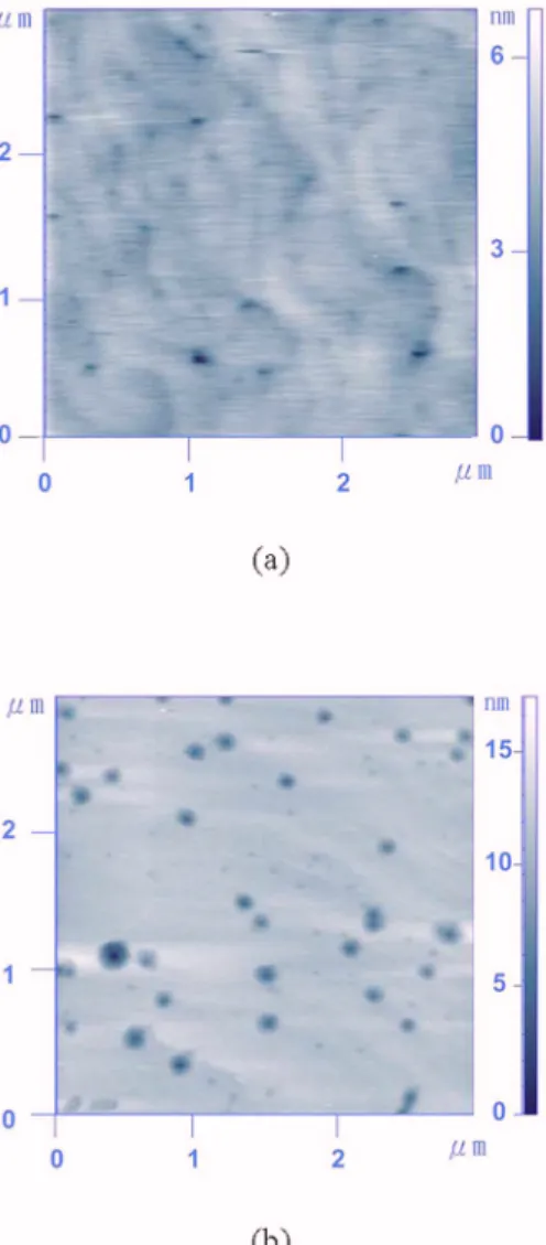
580 ° C followed by a LT SiN layer. The growth time of the LT SiN layer was 300 s. We then raised the temperature to 1020 ° C to grow a 2-m-thick GaN epitaxial layer 共i.e., sample A兲. For comparison, samples without the SiN layer were also prepared 共i.e., sample B兲. After the growth, we performed etch pit study for these two samples. Figures1共a兲 and1共b兲show atomic force microscope共AFM兲 images of the etched samples A and B, respectively. From these AFM im-ages, it was found that etch pit density was 9.2⫻108cm−2 for sample B with conventional LT GaN nucleation layer. In contrast, etch pit density was only 3.3⫻108cm−2for sample A. These values indicate that we can indeed reduce disloca-tion density in GaN epitaxial layer by inserting the LT SiN layer. SBPDs were then fabricated. After mesa etching for 0.5m, we deposited Ti共15 nm兲/Al共400 nm兲 as the Ohmic contact, and subsequently thermally annealed at 700 ° C for 5 min for alloying. Ni共3 nm兲/Au共6 nm兲 was used as the Schottky contact material.
Figure2shows dark current-voltage共I-V兲 characteristics of the fabricated SBPD. With −5 V applied bias, it was found that reverse leakage current of sample A was 7.8 ⫻10−12A, while that of sample B was four orders of mag-nitude larger. It should be noted that leakage current of sample B depends strongly on reverse bias. The much smaller and much less voltage dependent leakage current ob-served from sample A should be attributed to the use of SiN / GaN nucleation layer. These results also suggest that we can reduce threading dislocation in the epitaxial layer and thus improve device performance by inserting the porous SiN layer. With the SiN / GaN nucleation layer, Schottky bar-rier height should be enhanced due to the reduction of trap levels within the band gap of GaN. According to the Norde method, the effective Schottky barrier height 共b兲 of these two samples can be determined by plotting F共V兲−V curves. The F共V兲 function is defined as15
a兲Electronic mail: [email protected]
APPLIED PHYSICS LETTERS 91, 103506共2007兲
0003-6951/2007/91共10兲/103506/3/$23.00 91, 103506-1 © 2007 American Institute of Physics
F共V兲 = V 2 − kT q ln
冉
I共V兲 AAⴱ ⴱ T2冊
, 共1兲where I共V兲 could be achieved from the I-V curves. From the minimum in the F共V兲−V curve, we can calculate the effec-tive Schottky barrier height by
b= F共Vmin兲 +
Vmin
2 −
kT
q , 共2兲
where F共Vmin兲 is the minimum point of F共V兲 and Vminis the corresponding voltage. Figure 3 shows F共V兲−V curves of
samples A and B which were replotted from Fig. 2. From these curves, it was found that the effective Schottky barrier heights of samples A and B were around 1.53 and 1.27 eV, respectively. These values agree with the aforesaid issue that larger barrier height resulted in the lower dark current in sample A, as compared with conventional SBPD with single LT GaN nucleation layer.
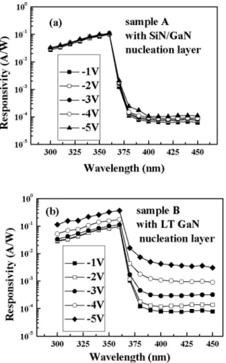
Figures4共a兲and4共b兲show spectral response of samples A and B, respectively. It can be seen that cutoff occurred at around 360 nm for both samples. With incident light wave-length of 360 nm and −1 V applied bias, it was found that measured responsivities for these two samples were both around 0.10 A / W. As shown in Fig.3共b兲, the responsivity of sample B increased to 0.37 A / W as the reverse bias was increased to −5 V. This suggests that some internal gain ex-ists in sample B, which probably originated from the thread-ing dislocation in the epitaxial layer.16 Very recently, it has been reported that internal gain in GaN-based SBPD is re-lated to the persistent photocurrent gain.17 In brief, disloca-tion related surface/interface traps in GaN epitaxial layers can act as generation-recombination centers. Other than the photovoltaic current, an additional current will be created by photogenerated holes drifting to the metal-semiconductor in-terface when SBPD was under illumination. The holes trapped at the surface sites produce net positive charges which will affect the equilibrium surface charge. This will reduce the depletion width and the build-in voltage to cause a lower Schottky barrier height. Thus, we observed a larger dark current from sample B. In contrast, the responsivity of sample A shown in Fig.3共b兲was almost independent of bias, implying the internal gain in sample A is much smaller. The experimental evidence again could be attributed to the di-minishing effect of threading dislocation owing to the use of SiN / GaN nucleation layer. Here, we define UV to visible rejection ratio as the responsivity measured at 360 nm di-vided by the responsivity measured at 420 nm. With −1 V reverse bias, it was found that UV to visible rejection ratios were 1.61⫻103and 1.25⫻103for samples A and B, respec-tively. As we increased the reverse bias to −5 V, it was found FIG. 1. 共Color online兲 AFM images of the etched 共a兲 sample A and 共b兲
sample B.
FIG. 2. Dark I-V characteristics of the fabricated SBPD.
FIG. 3. F共V兲-V curves of samples A and B which were replotted from Fig. 2.
103506-2 Jhou et al. Appl. Phys. Lett. 91, 103506共2007兲
that UV to visible rejection ratios became 1.07⫻103 and 1.00⫻102 for samples A and B, respectively. The findings indicate an enhancement of UV to visible rejection ratio as result of inserting a LT SiN layer into the photodetector. It also indicates that such enhancement is more pronounced when the photodetectors were operated at large reverse bias. In summary, GaN Schottky barrier photodetectors with SiN / GaN nucleation layer were fabricated. It was found that leakage current was much smaller and much less bias
depen-dent for the photodetector with SiN / GaN nucleation layer, as compared to the photodetector with conventional LT GaN nucleation layer. It was also found that effective Schottky barrier height increased from 1.27 to 1.53 eV with the inser-tion of the SiN layer. Furthermore, it was found that we can effectively suppress internal gain of the detector and enhance UV to visible rejection ratio by using the SiN / GaN nucle-ation layer.
1S. Nakamura, M. Senoh, S. Nagahama, N. Iwasa, T. Yamada, T. Mat-sushita, H. Kiyoku, Y. Sugimuto, T. Kozaki, H. Umemoto, M. Sano, and K. Chocho, Appl. Phys. Lett. 72, 211共1998兲.
2S. J. Chang, W. C. Lai, Y. K. Su, J. F. Chen, C. H. Liu, and U. H. Liaw, IEEE J. Sel. Top. Quantum Electron. 8, 278共2002兲.
3N. Biyikli, I. Kimukin, O. Aytur, and E. Ozbay, IEEE Photonics Technol. Lett. 16, 1718共2004兲.
4C. K. Wang, S. J. Chang, Y. K. Su, Y. Z. Chiou, S. C. Chen, C. S. Chang, T. K. Lin, H. L. Liu, and J. J. Tang, IEEE Trans. Electron Devices 53, 38 共2006兲.
5O. Katz, V. Garber, B. Meyler, G. Bahir, and J. Salzman, Appl. Phys. Lett. 80, 347共2002兲.
6S. J. Chang, C. L. Yu, R. W. Chuang, P. C. Chang, Y. C. Lin, Y. W. Jhan, and C. H. Chen, IEEE Sens. J. 6, 1043共2006兲.
7E. Monroy, E. Muňoz, F. J. Sánchez, F. Calley, E. Calleja, B. Beaumont, P. Gibart, J. A. Muňoz, and F. Cussó, Semicond. Sci. Technol. 13, 1042 共1998兲.
8G. Y. Xu, A. Salvador, W. Kim, Z. Fan, C. Lu, H. Tang, H. Morkoç, G. Smith, M. Estes, B. Goldenberg, W. Yang, and S. Krishnankutty, Appl. Phys. Lett. 71, 2154共1997兲.
9K. Uchida, K. Nishida, M. Kondo, and H. Munekata, J. Cryst. Growth 189-190, 270共1998兲.
10T. Kachi, K. Tomita, K. Itoh, and H. Trando, Appl. Phys. Lett. 72, 704 共1998兲.
11S. Sakai, T. Wang, Y. Morishima, and Y. Naoi, J. Cryst. Growth 221, 334 共2000兲.
12C. H. Kuo, S. J. Chang, Y. K. Su, C. K. Wang, L. W. Wu, J. K. Sheu, T. C. Wen, W. C. Lai, J. M. Tsai, and C. C. Lin, Solid-State Electron. 47, 2019 共2003兲.
13S. J. Chang, C. S. Chang, Y. K. Su, R. W. Chuang, Y. C. Lin, S. C. Shei, H. M. Lo, H. H. Y. Lin, and J. C. Ke, IEEE J. Quantum Electron. 39, 1439 共2003兲.
14S. J. Chang, L. W. Wu, Y. K. Su, Y. P. Hsu, W. C. Lai, J. M. Tsai, J. K. Sheu, and C. T. Lee, IEEE Photonics Technol. Lett. 16, 1447共2004兲. 15H. Norde, J. Appl. Phys. 50, 5052共1979兲.
16O. Katz, V. Garber, B. Meyler, G. Bahir, and J. Salzman, Appl. Phys. Lett. 79, 1417共2001兲.
17N. Vanhove, J. John, A. Lorenz, K. Cheng, G. Borghs, and J. E. M. Haverkort, Appl. Surf. Sci. 253, 2930共2006兲.
FIG. 4. Spectral response of共a兲 sample A and 共b兲 sample B.
103506-3 Jhou et al. Appl. Phys. Lett. 91, 103506共2007兲