Interfacial bonding behavior with introduction of Sn–Zn–Bi
paste to Sn–Ag–Cu ball grid array package during
multiple reflows
Po-Cheng Shih and Kwang-Lung Lina)
Department of Materials Science and Engineering, National Cheng-Kung University, Tainan, Taiwan 701, Republic of China
(Received 20 July 2004; accepted 18 October 2004)
Sn–8Zn–3Bi solder paste and Sn–3.2Ag–0.5Cu solder balls were reflowed
simultaneously on Cu/Ni/Au metallized ball grid array (BGA) substrates to investigate the interfacial bonding behaviors for multiple reflow cycles at two different soldering temperature of 210 and 240 °C. The different intermetallic compounds that formed at the interface after one reflow cycle were respectively the island-shaped Ag–Au-Cu-Zn (near the solder) compounds and the Ni–Sn–Cu-Zn (near the metallized pad)
compounds in 210 or 240 °C soldering systems. Layered Ag–Au–Cu–Zn, Ag5Zn8, and Ag–Zn–Sn compounds were also observed within the solder near the interface after single reflow cycle. After ten reflow cycles, the Ag–Au–Cu–Zn compounds
significantly decomposed, while the Ag3Sn and Ni–Sn–Cu–Zn compounds coarsened obviously.
I. INTRODUCTION
Sn–Pb solder alloys have been widely used in elec-tronic packaging industries due to their low eutectic melting temperatures (around 183 °C) and good wetting behavior on several substrates such as Cu, Ag, Pd, and Au.1–3 However, the Pb contained in these solders is toxic and detrimental to the environment and to human health. As a result, the use of Pb-free solders will soon be required for the manufacture of electronic products, driv-ing the need for a Sn–Pb solder substitutent. Among the potential candidates for lead-free solders, Sn–Ag–Cu holds promise because of its good resistance to thermal fatigue, high ductility,4and better solderability on copper than Sn–Pb solder.5 However, the ternary eutectic position of Sn–Ag–Cu solder takes place within the com-position range of 3.2–4.7 wt% Ag and 0.5–1.7 wt% Cu at 217 °C,5 which is about 40 °C higher than that of Sn–Pb eutectic solder. This is expected to result in the excessive growth of intermetallic compounds (IMCs) during the soldering process.6
The overgrown IMCs are known to be detrimental to the bonding strength between the solder and the substrate due to increased brittleness. To overcome this problem, a nickel layer is often used as a diffusion barrier to prevent copper from diffusing into the solder to form the IMCs. A gold layer, plated on the
Ni layer of the metallized pads, not only improves wet-tability but also increases oxidation resistance.7
Sn–Zn solder (Sn–9mass% Zn for the eutectic compo-sition), with a eutectic melting temperature of 199 °C,
a)
Address all correspondence to this author. e-mail: [email protected] DOI: 10.1557/JMR.2005.0023
FIG. 1. The cross-sectional schematic of the specimen before reflow process.
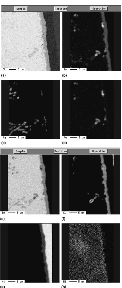
FIG. 2. The elemental analysis at the interfacial area of the single reflow specimen soldered at 210 °C (a) backscattered electron image, (b) Zn, (c) Au, (d) Ag, (e) Sn, (f) Cu, (g) Ni, and (h) Bi.
has also been recommended as a lead-free solder for replacing Sn–Pb eutectic solder.8,9 Moreover, the addi-tion of Bi to Sn–Zn near eutectic solder can improve the soldering properties by lowering melting temperature to roughly 188–199 °C.10–12
With the results mentioned above, the soldering tem-perature of Sn–Ag–Cu could be decreased with the in-troduction of Sn–Zn–Bi solder paste. The lowering in reflow temperature with the intermediate Sn–Zn–Bi paste could inhibit the excessive growth of IMCs by Sn–Ag–Cu. The purpose of this study is to investigate the interfacial interactions of the materials when the com-mercial Sn–Zn–Bi solder paste is introduced to the Sn– Ag–Cu soldering system for single reflowed and multiple reflowed specimens. In addition, the effect of the differ-ent soldering temperatures on the interaction behavior of the solder alloys will be examined for multiple reflows.
II. EXPERIMENTAL PROCEDURE
Commercial Sn–8Zn–3Bi solder paste and Sn–3.2Ag– 0.5Cu (mass%) solder balls were used in this study. The solder paste and solder balls were reflowed simulta-neously on Cu/Ni/Au metallized ball grid array (BGA) substrates. The solder paste was composed of activated flux and Sn–Zn–Bi solder particles, which were 20–25m in diameter. The solder balls were 760 m in
diameter. The thickness of the gold layer was less than 1m, while the nickel and copper layers were about 7 m and 30 m thick, respectively. A stencil printing machine was used to apply solder paste to each Cu/Ni/Au metallized solder pad on the substrate, and then a solder ball was located on each paste-covered pad, as shown in Fig. 1.
The specimens were divided into two sets; one set was reflowed at 210 °C while the other set was reflowed at 240 °C. Within each set, separate groups were reflowed 1, 5, and 10 times. The reflow experiment was performed in an infrared (IR) furnace using a protective atmosphere of 90% N2–10% H2. The reflow profile consisted of ac-tivation at 170 °C with a peak temperature of 210 or 240 °C for 30 s and afterward descended to room tem-perature through 3–4 min. Multiple reflows of the solder balls were conducted by repeating the reflow temperature profile for the desired number of cycles. The BGA speci-mens were mounted, polished with 0.3-m Al2O3 pow-der, and then etched with a 5% HCl–95% H2O solution for interfacial investigation by scanning electron micros-copy (SEM), energy dispersive x-ray analysis (EDX), and electron probe microanalysis (EPMA). Moreover, to easily identify the crystal phases of the IMCs of BGA samples observed in either 210 or 240 °C soldering sys-tems, the x-ray diffractometer analysis was carried out by employing the Cu/Ni/Au foils instead of
FIG. 3. The SEM images of the IMCs formed after single reflow at 210 °C: (a) the layer compound [A: the upper part, B: the lower part], (b) the island-shaped compound [labeled C], (c) solder ball, and (d) the magnified image of D region in (c).
substrate. Thickness of the Ni layer is 3m, and that of Au is less than 1m. Ammonia solution was used to etch away the Cu for x-ray analysis.
III. EXPERIMENTAL RESULTS
Identifications of the IMCs with the interaction of the materials
The cross-sectional SEM image of the single reflow specimen soldered at 210 °C is shown in Fig. 2(a). El-emental mapping analysis [Figs. 2(b)–2(h)] reveals that discontinuous discrete particulate IMCs formed at the interface between the Cu/Ni/Au metallization layers and solder. These IMCs consist of Ni, Sn, Cu, and Zn. It is likely that Ag and Au are incorporated with these com-pounds. Meanwhile, the needle-shaped Ag–Zn–Sn and Ag–Zn compounds are observed in the solder region. Moreover, a relatively thick layer compound composed of Ag, Au, Cu, and Zn with varying elemental distribu-tion forms near the interface. It seems to show that Ag– Sn IMC particles are embedded within this compound layer. The Bi distributes uniformly in the solder and does not associate with any compound. It is noticed that the region between the Ag–Au-Cu-Zn and the Ni-Sn–Cu-Zn compound layers consist of Sn and Bi only. Zn of the Sn–8Zn–3Bi solder paste migrates outward and inward completely to form the IMCs. Figures 3(a)–3(b) show the IMCs formed between the solder and the metallized pad. The energy dispersive spectroscopy (EDS) results show that composition ratio of the compounds A and B are, respectively, Ag:Au:Cu:Zn⳱ 10:7:20:63 and 7:17:12:64 (at.%), which correspond to the EPMA results for Ag, Au, and Cu elemental distributions of the layer IMCs in Figs. 2(b)–2(d) and 2(f). The composition of the island-shaped compound of Fig. 3(b) (labeled C) is Ag:Au:Cu:Zn ⳱ 10:6:22:62 (at.%), and the needle-shaped compounds are identified as Ag5Zn8. Figure 3(d), a magnification of region D in Fig. 3(c), reveals that there are Ag3Sn particles in the upper part of the solder ball. Reflow resulted in counter diffusion between the Sn– Ag–Cu solder ball and the Sn–Zn–Bi solder paste. The two originally separated solders mixed together and did not show visible interfacial boundary, as shown in Fig. 3(c).
The Ni–Sn–Cu-Zn compounds (roughly Ni:Sn:Cu:Zn⳱ 27:43:13:16, at.%), shown in Figs. 4(a) and 4(b), slight-ly grew upon multiple reflow. While the layer Ag–Au– Cu–Zn compounds observed in the single reflow speci-men break into smaller pieces and detach from the un-derneath Ni–Sn–Cu–Zn compound after 5 reflow cycles at a soldering temperature of 210 °C, as shown in Fig. 4(a). The layer Ag–Au–Cu–Zn compounds shrink and almost disappear after 10 reflow cycles at 210 °C, as shown in Fig. 4(b). The Ag3Sn grows and coarsens sig-nificantly after 10 reflow cycles, as comparing the results
FIG. 4. The SEM images of the IMCs formed for reflow at 210 °C, (a) 5 reflow cycles, (b, c) 10 reflow cycles.
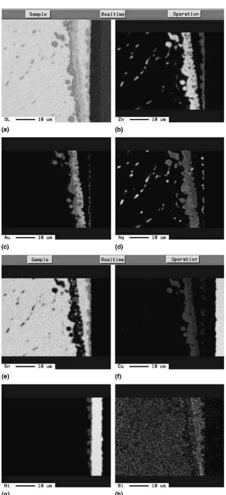
FIG. 5. The elemental analysis at the interfacial area of the specimen soldered at 210 °C after 10 reflow cycles (a) backscattered electron image, (b) Zn, (c) Ag, (d) Au, (e) Sn, (f) Cu, (g) Ni, and (h) Bi.
FIG. 6. The Zn–containing compounds shrink after multiple reflow, (a, b) single reflow cycle, and (c) 10 reflow cycles.
FIG. 7. The SEM images of the IMCs formed at the interface after reflow at 240° C for (a, b) single reflow, (c) 5 reflow cycles, and (d) 10 reflow cycles.
FIG. 8. The elemental analysis at the interfacial area of the specimen soldered at 240 °C after 5 reflow cycles (a) backscattered electron image, (b) Zn, (c) Ag, (d) Au, (e) Sn, (f) Cu, (g) Ni, and (h) Bi.
of Figs. 3(d) and 4(c). Figure 5(a) shows the cross-sectional image of the specimen reflowed for ten cycles at 210 °C. It shows a segregation behavior of Bi in the solder near the interface, as shown in Fig. 5(h). This segregation behavior is not in association with any other elements. Besides this, Bi was seen to distribute through the solder layer. Zn forms the Ni–Sn–Cu–Zn IMC at the interface. The elemental analysis indicates that Zn seems to form IMC with Ag in the region closing to interface. This IMC is likely to have Au, Cu, and Sn dissolved in it. However, Zn seems to dissolve in the Ag3Sn com-pound in the bulk solder, as revealed in Fig. 6. Moreover, Zn atoms gradually migrate out of the dispersive Ag– Zn–Sn compounds during multiple reflow and seem to lead to the coarsening of the Ag3Sn compounds, as shown in Figs. 6(a)–6(c).
Figures 7(a) and 7(b) show the cross-sectional image of the single reflow specimen soldered at 240 °C. As with the 210 °C soldering system, the island-shaped and the elongated compounds, whose compositions are quite close to those in 210 °C single reflow specimen, are also observed. Figure 7(c) shows that the IMCs located at the interface are mainly Ni–Sn–Cu–Zn compounds (Ni:Sn: Cu:Zn⳱ 26:44:12:17, at.%), which formed in a continu-ous layer (about 3–5m thick) and some detached from
this layer and moved into the solder after 5 reflow cycles. The elemental mapping analysis also shows similar re-sults, as shown in Fig. 8. Meanwhile, as found in the 210 °C cases above, the Ag–Au–Cu–Zn compounds also decompose into smaller pieces circled. For 10 reflow cycles at a 240 °C soldering temperature, Ni–Sn–Cu–Zn compounds reach a thickness of 4–9 m with some pieces of these compounds suspended in the solder, as shown in Fig. 7(d).
Figure 9 shows the x-ray diffraction (XRD) data for specimens reflowed at 210 and 240 °C for 1 and 10 reflow cycles. Similar results are obtained for the phase peaks of Ni3Sn4, CuZn, AgZn3, and AuZn3compounds at 210 and 240 °C for the single reflow soldering system, while the peaks of AgZn3and AuZn3compounds are not distinct after ten reflow cycles.
IV. DISCUSSION
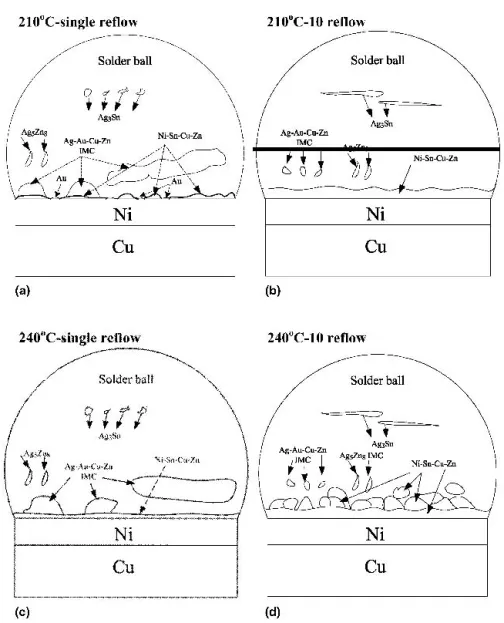
Based on observations and analysis of the interfacial IMCs, a possible interaction between the two solders and substrate can be described, as shown in Fig. 10. Figures 10(a) and 10(b) and Figs. 10(c) and 10(d) are respec-tively the schematic diagrams of the interfacial IMCs formation between the two solders and Cu/Ni/Au metal-lized solder pads at 210 and 240 °C soldering tempera-tures. Previous studies12–14 indicated that the activation energy of diffusion of Sn in a Cu matrix (177 kJ/mol) is much higher than that of Cu in a Sn matrix (33.02 kJ/ mol). The diffusion constant of Cu or Zn atoms in Sn crystals is significantly larger than that of the self-diffusion of Sn. Meanwhile, the magnitude of diffusivity of Cu in a Sn matrix is 1,000–10,000 times larger than that of Zn. This difference enables Cu atoms to move through the Sn matrix during the soldering process and leads to the formation of Cu-containing compounds near the interface between the solder and the Cu/Ni/Au met-allized pads, as shown in Figs. 10(a) and 10(c). It was also indicated4 that Au reacts easily with Zn to form Au–Zn intermetallic compounds. Hence, according to the XRD experimental results and the binary phase diagram of Ag–Au, Ag–Zn, and Au–Zn,15–17the Ag–Au–Cu–Zn compounds may consist of AuZn3 and AgZn3 com-pounds with Ag and Au substituting freely. On the other hand, the solubility of Zn in Cu at 200 °C is at most 33 at.%.18 Au and Cu also have a solid solution at 200 °C.19However, Cu and Ag are hardly interact with each other.20 The Ag–Au–Cu–Zn compound could be composed of the (Ag, Au)Zn3and a solution containing Zn, Au, and Cu atoms of which the proportions vary by location. The CuZn peaks appeared in the XRD results of the single reflow samples. Hence, CuZn compounds may exist in Ag–Au–Cu–Zn or Ni–Sn–Cu–Zn IMCs or both. The detailed microstructure of the Ag–Au–Cu–Zn com-pounds needs to be further investigated. Figures 10(a)
FIG. 9. XRD patterns of the interfacial compounds formed between the solder and the substrate at different soldering temperature for de-sired reflow cycles.
and 10(c) show similar results except that some Au nod-ules did not diffuse away from the interface in single reflow due to the various diffusivities affected by a 30 °C difference in soldering temperature. After 10 reflow cycles in both soldering systems, the Ag–Au–Cu–Zn compounds seem to decompose into small dispersed par-ticles. The reasons for the decomposition of Ag–Au–Cu– Zn compounds are not clear. Ag might diffuse to enhance the growth of Ag3Sn, as shown in Figs. 4(c) and 6(c), and Au might dissolve into the solder after multiple reflow cycles because of the high solubility of Au in the molten solder.21
Moreover, the Au–Sn compounds could have formed,22
but they are not observed in this study. The Cu and Zn atoms diffuse into the interface causing signifi-cant growth of Ni–Sn–Cu–Zn compounds after ten re-flow cycles, as shown in Figs. 4(b) and 7(d). On the other hand, the decrease in the Zn content of the Ag–Zn–Sn IMCs may relate to the growth of the Ni–Sn–Cu–Zn IMC.
The Ni–Sn–Cu–Zn compounds, formed closing to the interface after single reflow cycle, mainly contain Ni and Sn. In addition, Ni–Sn–Cu–Zn compounds grow faster at higher soldering temperatures, and some even spall into the solder. According to the XRD data, the detecting incident x-ray moving through the Cu/Ni/Au foil first, the AgZn3 and AuZn3 almost disappear due to the sig-nificant decomposition of Ag–Au–Cu–Zn compounds, while the CuZn peaks are obvious in ten reflow samples. It may be attributed to that the Ni–Sn–Cu–Zn IMCs con-sist of Ni3Sn4and CuZn. Previous studies
23–27
indicated that Cu could react with Sn to form Cu–Sn compounds. However, in this study, Cu–Zn compounds are observed instead of Cu–Sn compounds. The Gibbs free energy of compound formation of Cu–Zn and Cu–Sn are −11.5 to −12.3 kJ/mol and −6.6 to −7.78 kJ/mol, respectively.8,28 From this point of view, Cu–Zn compounds are more stable than Cu–Sn compounds. The Gibbs free energy
FIG. 10. The sketches of the IMCs formed at different soldering temperature for (a) 210 °C-single reflow, (b) 210 °C-10 reflows, (c) 240 °C-single reflow, and (d) 240 °C-10 reflows.
may not absolutely govern the interfacial reaction during soldering as the reaction does not reach equilibrium. However, the formation of Cu–Zn compounds, but not Cu–Sn compounds, is also indicated by the thermody-namic analysis results.
Other interfacial reaction results in the Sn–Ag/Ni, Sn– Cu/Ni, and Sn–Ag–Cu/Ni systems7,23–25,29
are compared with those in this study. In the case of the Sn–3.5 (3.9) Ag solder system, the IMC phase formed at the interface was Ni3Sn4. In the Sn–4.0Ag–0.5Cu solder system, the IMC formed at the interface was composed of Cu, Ni, and Sn. It means that a small amount of Cu in Sn–Ag–Cu alloy significantly affected interfacial reaction. In the case of Sn–4.0Ag–0.5Cu and Sn–0.7Cu solders, the IMC phases found at the interface were respectively (Cu, Ni)6Sn5and (Ni, Cu)3Sn4, with the involvement of Ni or Cu in Cu6Sn5 or Ni3Sn4, completely different from the Ni3Sn4IMC observed in Sn–3.5 (3.9) Ag solder.
A comparison between the results of the present study and those reported that the introduction of Zn tends to change the compound formation. Zn becomes more im-portant than the Sn in compound formation. This behav-ior was also observed in the Sn–Zn solder system.9
V. CONCLUSIONS
The Sn–3.2Ag–0.5Cu BGA soldering temperature is successfully lowered down to 210 °C with the introduc-tion of commercial Sn–8Zn–3Bi solder paste during mul-tiple-reflow tests. The island-shaped Ag–Au–Cu–Zn (near the solder) compounds and the Ni–Sn–Cu–Zn (near the metallized pad) compounds were formed at the inter-face after single reflow at 210 and 240 °C. Layered Ag– Au–Cu–Zn, needle-shaped Ag5Zn8, and Ag–Zn–Sn com-pounds are also observed within the solder near the in-terface for single reflow cycle. After ten reflow cycles, the Ag–Au–Cu–Zn compounds significantly shrink, while the Ag3Sn and Ni–Sn–Cu–Zn compounds grow.
ACKNOWLEDGMENTS
The financial support for this work, provided by the National Science Council of Taiwan, Republic of China, under Grant No. NSC91-2216-E-006-035 is gratefully acknowledged. The authors also thank Accurus Scientific Co., LTD. for supplying the solder balls.
REFERENCES
1. M. Amagai, M. Watanabe, M. Omiya, K. Kishimoto, and T. Shibuya: Mechanical characterization of Sn–Ag–based lead-free solders. Microelectron. Reliab. 42, 951 (2002).
2. A. Hirose, T. Fujii, T. Imamura, and K.F. Kobayashi: Influence of interfacial reaction on reliability of QFP joints with Sn–Ag based Pb free solders. Mater. Trans. 42, 794 (2001).
3. Y. Miyazawa and T. Ariga: Influences of aging treatment on mi-crostructure and hardness of Sn–(Ag, Bi, Zn) eutectic solder al-loys. Mater. Trans. 42, 776 (2001).
4. Y. Chonan, T. Komiyama, J. Onuki, R. Urao, T. Kimura, and T. Nagano: Influence of P content in electroless plated Ni-P alloy film on interfacial structures and strength between Sn–Zn solder and plated Au/Ni-P alloy film. Mater. Trans. 43, 1887 (2002). 5. C.M. Chuang, P.C. Shih, and K.L. Lin: Mechanical strength of
Sn–3.5Ag–based solders and related bondings. J. Electron. Mater. 33,1 (2004).
6. S.K. Kang, W.K. Choi, D.Y. Shih, P. Lauro, D.W. Henderson, T. Gosselin, and D.N. Leonard: Interfacial reactions, microstruc-ture and mechanical properties of Pb-free solder joints in PBGA Laminates, in Electronic Components and Technology
Confer-ence, Institute of Electrical and Electronics Engineers, Inc, San
Diego, CA, 2002 Proceedings 52nd, 28-31 May 2002, pp. 146–153. 7. C.B. Lee, S.B. Jung, Y.E. Shin, and C.C. Shur: Effect of isother-mal aging on ball shear strength in BGA joints with Sn–3.5Ag–0.75Cu solder. Mater. Trans. 43, 1858 (2002). 8. S.P. Yu, H.J. Lin, M.H. Hon, and M.C. Wang: Effects of process
parameters on the soldering behavior of the eutectic Sn–Zn solder on Cu substrate. J. Mater. Sci.–Mater. Electron. 11, 461 (2000). 9. K. Suganuma, K. Niihara, T. Shoutoku, and Y. Nakamura: Wet-ting and interface microstructure between Sn–Zn alloys and Cu. J.
Mater. Res. 13, 2859 (1998).
10. T. Taguchi, R. Kato, A. Okuno, H. Suzuki, T. Okuno, and S. Akita: Lead free interfacial structures and their relationship to Au plating (including accelerated thermal cycle testing of non-leaden BGA spheres), in Electronic Components and Technology
Conference, Institute of Electrical and Electronics Engineers, Inc,
Orlando, FL, 2001 Proceedings, 51st, 29th May-1st June 2001, Orlando, FL, pp. 675–680.
11. Y.S. Kim, K.S. Kim, C.W. Hwang, and K. Suganuma: Effect of composition and cooling rate on microstructure and tensile prop-erties of Sn–Zn–Bi alloys. J. Alloys Compd. 352, 237 (2003). 12. I. Shohji, T. Nakamura, F. Mori, and S. Fujiuchi: Interface
reac-tion and mechanical properties of lead-free Sn–Zn alloy/Cu joints.
Mater. Trans. 43, 1797 (2002).
13. H.M. Lee, S.W. Yoon, and B.J. Lee: Thermodynamic prediction of interface phases at Cu/solder joints. J. Electron. Mater. 27, 1161 (1998).
14. S.W. Yoon, W.K. Choi, and H.M. Lee: Interfacial reaction be-tween Sn–1Bi-5In-9Zn solder and Cu substrate. Scripta Mater. 40, 327 (1999).
15. T.B. Massalski: Binary Alloy Phase Diagrams (ASM, Metals Park, OH, 1986), Vol. 1, pp. 5–7.
16. T.B. Massalski: Binary Alloy Phase Diagrams (ASM, Metals Park, OH, 1986), Vol. 1, pp.85–86.
17. T.B. Massalski: Binary Alloy Phase Diagrams (ASM, Metals Park, OH, 1986), Vol. 1, pp. 337–338.
18. T.B. Massalski: Binary Alloy Phase Diagrams (ASM, Metals Park, OH, 1986), Vol. 1, pp. 980–981.
19. T.B. Massalski: Binary Alloy Phase Diagrams (ASM, Metals Park, OH, 1986), Vol. 1, pp. 253–254.
20. T.B. Massalski: Binary Alloy Phase Diagrams (ASM, Metals Park, OH, 1986), Vol. 1, pp. 18–19.
21. F. Zhang, M. Li, C.C. Chum, and Z.C. Shao: Effects of substrate metallization on solder/under-bump metallization interfacial reac-tions in flip-chip packages during multiple reflow cycles. J.
Elec-tron. Mater. 32, 123 (2003).
solder joints in electronic packaging technology. Mater. Sci. Eng.
R 38, 55 (2002).
23. C.E. Ho, R.Y. Tsai, Y.L. Lin, and C.R. Kao: Effect of Cu concen-tration on the reactions between Sn–Ag–Cu solders and Ni.
J. Electron. Mater. 31, 584 (2002).
24. Y.D. Jeon, S. Nieland, A. Ostmann, H. Reichl, and K.W. Paik: Studies on the interfacial reactions between electroless Ni UBM and 95.5Sn–4.0Ag–0.5Cu alloy, in Electronic Components and
Technology Conference, Institute of Electrical and Electronics
En-gineers, Inc, San Diego, CA, 2002 Proceedings 52nd, 28-31 May 2002, pp. 740–746.
25. A. Zribi, A. Clark, L. Zavalij, P. Borgesen, and E.J. Cotts: The growth of intermetallics compounds at Sn–Ag–Cu solder/Cu and Sn–Ag–Cu solder/Ni interfaces and the associated evolution of the solder microstructure. J. Electron. Mater. 30, 1157 (2001). 26. Y. Zheng, C. Hillman, and P. McCluskey: Intermetallic growth on
PWBs soldered with Sn3.8Ag0.7Cu, in Electronic Components
and Technology Conference, Institute of Electrical and Electronics
Engineers, Inc., San Diego, CA, 2002 Proceedings 52nd, 28-31 May 2002, pp. 1226–1231.
27. K.S. Kim, S.H. Huh, and K. Suganuma: Effects of fourth alloying additive on microstructures and tensile properties of Sn–Ag–Cu alloy and joints with Cu. Microelectron. Reliab. 43, 259 (2003). 28. S.P. Yu, M.C. Wang, and M.H. Hon: Formation of intermetallic compounds at eutectic Sn–Zn–Al solder/Cu interface. J. Mater.
Res. 16, 76 (2001).
29. K.W. Paik, Y.D. Jeon, and M.G. Cho: Interfacial reactions and bump reliability of various Pb-free solder bumps on electroless Ni-P UBMs, in Electronic Components and Technology
Confer-ence, Institute of Electrical and Electronics Engineers, Inc, Las
Vegas, NV, 2004 Proceedings 54th, pp. 675–682.

![FIG. 3. The SEM images of the IMCs formed after single reflow at 210 °C: (a) the layer compound [A: the upper part, B: the lower part], (b) the island-shaped compound [labeled C], (c) solder ball, and (d) the magnified image of D region in (c).](https://thumb-ap.123doks.com/thumbv2/9libinfo/8997192.284572/3.945.212.728.126.583/formed-single-reflow-compound-compound-labeled-magnified-region.webp)