國 立 交 通 大 學
機械工程學系
博士論文
電鍍鎳基奈米鑽石與奈米碳管複合材料於微機械式
共振器之應用
Electroplated Ni-diamond and Ni-CNT nanocomposites for
micromechanical resonator applications
研 究 生:李毅家
指導教授:徐文祥 教授
鄭裕庭 教授
電鍍鎳基奈米鑽石與奈米碳管複合材料於微機械式共振器之應用
Electroplated Ni-diamond and Ni-CNT nanocomposites for
micromechanical resonator applications
研 究 生:李毅家 Student:Yi-Chia Lee
指導教授:徐文祥 Advisor:Wensyang Hsu
鄭裕庭 Yu-Ting Cheng
國立交通大學
機械工程學系
博士論文
A ThesisSubmitted to Department of Mechanical Engineering College of Engineering
National Chiao Tung University In Partial Fulfillment of the Requirements
For the Degree of PhD In
Mechanical Engineering July 2012
電鍍鎳基奈米鑽石與奈米碳管複合材料於微機械式共振器之應用
學生:李毅家 指導教授:徐文祥
鄭裕庭
國立交通大學機械工程學系 博士班
摘 要
在無線通訊與消費電子系統的應用上,石英共振器為重要的時間或頻率的參考源, 但石英共振器在製程上難與其他電路做直接性的整合。相較之下,微機械式共振器展現 高度的製程整合性,使其逐漸取代石英共振器之應用。本論文首先提出以電鍍鎳基奈米 鑽石粒子與奈米碳管兩種奈米複合材料,製作微機械式共振器。為了完全利用奈米粒子 (奈米鑽石粒子與奈米碳管)的特性,奈米粒子必須在電鍍液中均勻分散。目前所使用的 奈米鑽石粒子能均勻分散於電鍍液中,而奈米碳管則呈現聚集狀態,需進行分散處理。 在此採用硫酸/過氧化氫與十二烷基硫酸鈉水溶液兩種配方做為奈米碳管的分散處理液。 由實驗結果可知,十二烷基硫酸鈉水溶液所處理的奈米碳管在分散狀態與鍍層中的含量 皆優於硫酸/過氧化氫處理,用於微機械式共振器的製作上,可得到較高的共振頻率提升。 製程上,鎳基奈米複合材料所製作之懸浮微結構常因為殘留應力導致翹曲。此翹曲問題 在此可藉由降低電鍍之電流密度而減緩。當電流密度為 0.8 mA/cm2時,可得到低應力梯 度之純鎳、鎳-奈米鑽石、鎳-奈米碳管,值各為-3.23、-5.65、-4.75 MPa/μm。相較於 15.3 mA/cm2電流密度,可降低 41~21%的應力梯度。由於奈米鑽石粒子(2 g/L)與奈米碳管(1 g/L)的添加,所得到的鎳基奈米複合材料各有 1.39 與 1.46 倍的楊氏係數/密度比值,高 楊氏係數/密度比值有助於提升共振器的共振頻率。在此採用梳狀與橋狀微機械式共振器 的結構設計。對於梳狀設計,鎳-奈米鑽石(2 g/L)與鎳-奈米碳管(0.028 g/L)相對於純鎳, 各提升 14% 與 8%的共振頻率;橋狀設計,共振頻率的提升量為 45% (2 g/L) 與 27% (1 g/L)。在共振頻率提升的同時,共振器的品質因子並不會因為奈米粒子的添加而大幅衰 減。Electroplated Ni-diamond and Ni-CNT nanocomposites for
micromechanical resonator applications
Student:Yi-Chia Lee Advisors:Wensyang Hsu
Yu-Ting Cheng
Department of Mechanical Engineering
National Chiao Tung University
Abstract
Quartz plays an important role for time and frequency reference in wireless and consumer electronic systems. Unfortunately, quartz resonator is not easy to integrate with other electronics directly. Currently, micromechanical resonator has become an alternative device to replace quartz resonator for better integration. Based on the technology trend, this dissertation explores the feasibility of electroplated Ni-diamond and Ni-CNT (Ni-Carbon Nanotube) nanocomposites for micromechanical resonator applications and proposes a proper fabrication process where good particle dispersion characteristics including nano diamonds and CNTs in electrolyte can be obtained to fully adopt the physical properties of the nano materials for achieving composite effects. The nano diamond and CNT particles can exhibit good dispersion using ultrasonication and the surface treatment of H2SO4/H2O2and SDS
water solution, respectively, that result in better frequency enhancement in nanocomposite micromechanical resonators. Meanwhile,as-plated Ni-based nanocomposite film is usually accompanied with residual stress that would cause significant undesired structural deformation. The stress issue can be evidently reduced by lowering plating current density.For the films plated with the density reduction from 15.3 mA/cm2to 0.8 mA/cm2, about 41%~21% stress gradient reduction can be realized. Experimental results show that the stress gradients are -3.23, -5.65, and -4.75MPa/μm for Ni, Ni-diamond, and Ni-CNT plate with 0.8 mA/cm2, respectively. The stress gradients are low enough to achieve a fully suspended micromechanical structure without any noticeable deformation. In addition, 39% and 46% ofE/ρenhancements can be achieved by the nano diamond (2 g/L) and CNTs (1 g/L) incorporations, respectively. The higher theE/ρ ratio is, the higher resonant frequency performance will be in the micromechanical resonators. Thus, in the work, comb and CC-beam designs are adopted for the validation of the performance improvement of the
致 謝
感謝所有曾經幫助、關心以及支持過我的所有人,因為有你們的協助,讓我在漫長 的研究路程上得以持續前進。 學術研究往往有無限的發展可能,正如同行舟於汪洋之中,雖可自在遨遊,卻總需 靠岸,而靠岸的關鍵在於方向與動力。我的指導教授,徐文祥老師與鄭裕庭老師扮演著 引導方向的重要角色,當我在研究上遇到瓶頸時,能及時提供我重要的建議;在問題探 討上,給予多面向的可能性分析;並指導我論文寫作的技巧,讓論文得以順利發表。此 外,感謝爸爸、媽媽以及眾多的家族成員,因為你們的關懷與支持,讓我有持續向目標 邁進的動力。同時也要感謝實驗室成員,包括君煒學長、涵評學長、梨暖學姐、駿偉學 長、家聖學長、育欣學長、元德學弟、一全學弟、盈斌學弟、松岳學弟、正鄴學弟以及 眾多實驗室的夥伴們,這一路的相互勉勵與陪伴,使我在研究的路上不覺得孤獨乏味。 除了方向與動力之外,也需要槳與舵的協助:交大奈米中心、國家晶片系統設計中 心,提供大量製程機台以及量測設備,讓我不必為了找尋實驗儀器而奔波;交大電子鄭 裕庭老師師門的趙子元同學與陳永昌學弟,協助場發射式電子顯微鏡的量測,使我能夠 快速得到材料性質的分析資料;清大奈微所李昇憲老師提供量測技術以及李銘晃學弟協 助電訊號的量測,讓我成功突破了量測上的困境。 其次要感謝口試委員,台大楊燿州老師、師大楊啟榮老師、清大李昇憲老師、交大 陳宗麟老師與鍾添淦老師以及兩位指導教授,在百忙之中撥空參與口試,提共寶貴的建 議,並對未來的發展提出更多的可能性。 回顧漫長的博士生生涯,也許論文內容並不完美,資料不夠完備,但卻讓我在這路 途的最終仍然努力不懈,並為下一階段的開始做準備。最後,希望本論文能對後續的相 關研究有所幫助,也期待實驗室的夥伴們能有更卓越的研究成果,與大家共勉。Table of Contents
摘 要 ... i Abstract ... ii 致 謝 ... iii Table of Contents ... iv Figure Captions ... vi Table Captions ... ix CHAPTER 1 INTRODUCTION ... 1 1.1FOREWORD ... 11.2BACKGROUND AND LITERATURES SURVEY ... 2
1.2.1 Micromechanical resonator ... 2
1.2.2 Electroplated Ni for micromechanical resonator application ... 4
1.2.3 Ni based nanocomposite ... 6
1.3THE SCOPE OF THIS DISSERTATION ... 7
CHAPTER 2 DESIGN AND FABRICATION OF RESONATOR ... 14
2.1DESIGN OF MICROMECHANICAL RESONATOR ... 14
2.1.1 Comb resonator ... 14
2.1.2 Clamped-clamped beam resonator ... 15
3.1.1 CNT surface modification... 25
3.2GRADIENT STRESS IN NI FILM ... 26
3.2.1 Gradient stress estimation ... 28
3.2.2 Grain boundary resulted stress ... 29
CHAPTER 4 CHARACTERIZATION OF MICROMECHANICAL RESONATOR ... 41
4.1MEASUREMENT SETUP ... 41
4.1.1 Optical measurement ... 41
4.1.2 Electrical measurement ... 42
4.2CHARACTERIZATION OF MICROMECHANICAL RESONATOR ... 43
4.2.1 Diamond and CNT incorporation ... 43
4.2.2 Performance measurement of comb resonators ... 43
4.2.3 Performance measurement of clamped-clamped beam resonators ... 45
4.2.4 Temperature coefficient of frequency ... 47
4.2.5 Power handling capability of CC-beam resonator ... 48
CHAPTER 5 CONCLUSION ... 65
5.1SUMMARY ... 65
5.2FUTURE WORK ... 66
REFERENCE ... 68
Figure Captions
Figure 1.1 Time and frequency components in GSM handset. ... 9
Figure 1.2 The commercial micromechanical resonator oscillators of (a) Discera and (b) SiTime. ... 9
Figure 1.3 (a) Comb resonator, (b) clamped-clamped beam, (c) free-free beam, (d) torsional resonator, and (e) disk resonator. ... 10
Figure 1.4 The frequency-Q product of micromechanical resonator over time. ... 10
Figure 1.5 Energy loss mechanisms of micromechanical resonator and their dependence on frequency. ... 11
Figure 1.6 Geometrically compensated folded-beam design for Ni comb resonator. ... 11
Figure 1.7 (a) Schematic of in situ localized anneal of Ni comb resonator. (b) Q is improved after localized anneal. ... 12
Figure 1.8 Fully monolithic CMOS Ni disk-array micromechanical resonator oscillator. (a) Overhead photo of oscillator and (b) 9 disk array resonator. ... 12
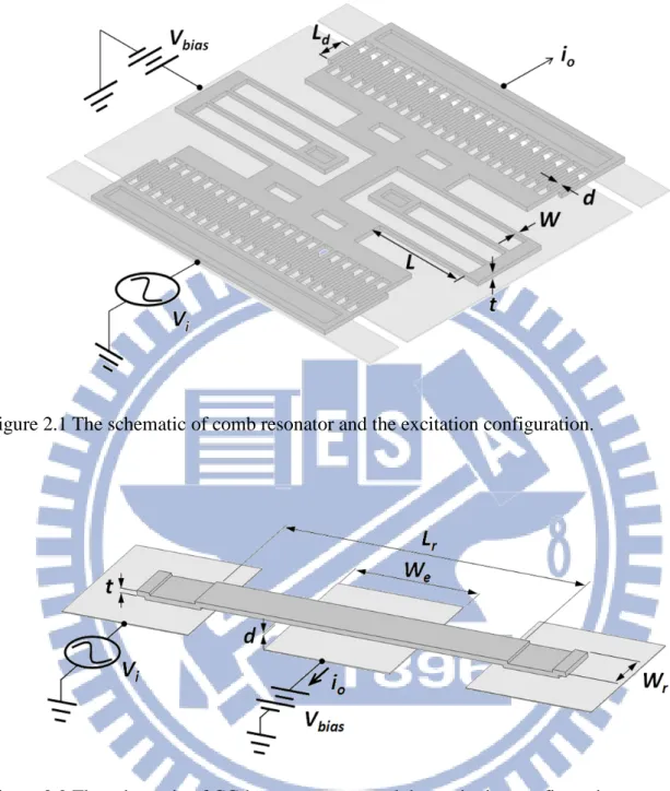
Figure 2.1 The schematic of comb resonator and the excitation configuration. ... 19
Figure 2.2 The schematic of CC-beam resonator and the excitation configuration. ... 19
Figure 2.3 Process flow of comb resonator. ... 20
Figure 2.4 Process flow of CC-beam resonator. ... 20
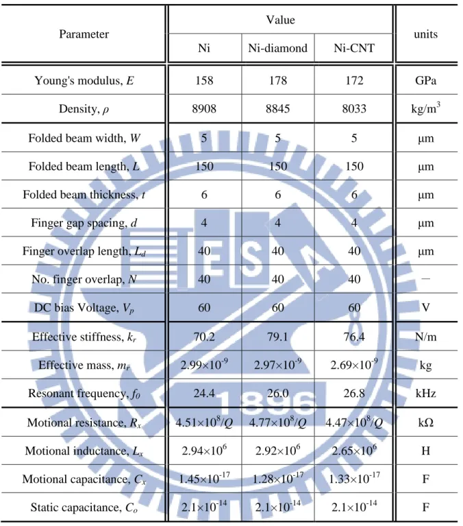
Figure 2.5 Electroplating system. The nano particles are kept in well dispersion in electrolyte with aerating system. ... 21
Figure 3.1 Nano particles for nanocomposite electroplating: (a) nano diamond particles in the preservation solution and (b) carbon nanotubes (CNTs) powder... 32
160min, and (d) 200 min. From left to right: H2SO4/H2O2, SDS water solution, and
DI water. ... 33 Figure 3.5 The CNTs treated by (a) DI water, (b) H2SO4/H2O2, and (c) SDS water solution and
spin dry on the Si wafer. ... 34 Figure 3.6 The comb resonator plated with 20 mA/cm2. The structure warps downward
seriously. The same dimension with thickness in (a) 6 μm, (b) 3 μm, and (c) 16 μm. ... 35 Figure 3.7 Micro-cantilever beam (a) before and (b) after release. (c) The stress distribution
can be expressed by the mean stress (σ0) and gradient stress (σ1) ... 36
Figure 3.8 (a) The surface profile of cantilever beams are characterized by
White-Light-Interferometer. (b) The cutting curve is extracted from the surface profile. (c) MATLAB is used to find the fitted curve and its value. ... 37 Figure 3.9 Long-short beam structure for mean stress characterization... 37 Figure 3.10 The stress gradient of Ni, Ni-diamond, and Ni-CNT nanocomposite films under
different current density. ... 38 Figure 3.11 (a) FIB cross sectional images of Ni films electroplated at 15.3 mA/cm2 and 0.8
mA/cm2 and Ni-diamond at 0.8 mA/cm2 (from left to right). (b) Model of grain evolution of electroplated Ni. ... 38 Figure 3.12 The grain size versus height: Ni plated at (a) 15.3 mA/cm2 and (b) 0.8 mA/cm2. (c)
Ni-diamond nanocomposite plated at 0.8 mA/cm2. ... 39 Figure 4.1 The in plane motion analysis of comb resonator by MEMS Motion Analyzer
(MMA). (a) The setup for displacement characterization of comb resonator. (b) The motion images captured by MMA. ... 50 Figure 4.2 The out of plane motion analysis of CC-beam resonator by Laser Doppler
Vibrometer (LDV). ... 51 Figure 4.3 Frequency characteristic measurement scheme of the CC-beam resonator. ... 51
Figure 4.4 SEM images of top surface of (a) Ni-diamond and (b) Ni-CNT nanocomposites. . 52 Figure 4.5 Volume percentage of nano particle in nanocomposite films: (a) Ni-diamond and (b)
Ni-CNT. ... 53 Figure 4.6 The SEM photos of (a) Ni, (b) Ni-diamond, and (c) Ni-CNT comb resonators
plated at 0.8 mA/cm2. ... 54 Figure 4.7 Frequency response for (a) Ni, (b) Ni-diamond, and (c) Ni-CNT comb resonators.
... 55 Figure 4.8 Frequency responses for (a) Ni, (b) Ni-CNT (H2SO4/H2O2), and (c) Ni-CNT (SDS)
comb resonators. ... 56 Figure 4.9 SEM photos and EDS analysis results of Ni-CNT comb resonators with CNTs
treated by H2SO4/H2O2 and SDS water solution. ... 57
Figure 4.10 The SEM photos of (a) Ni, (b) Ni-diamond, and (c) Ni-CNT CC-beam resonators plated at 0.8 mA/cm2. ... 58 Figure 4.11 Frequency characteristics for (a) Ni, (b) Ni-diamond, and (c) Ni-CNT CC-beam
resonators at 0.2 mTorr. ... 59 Figure 4.12 The resonant frequency shift versus temperature. ... 60
Table Captions
Table 1.1 Material properties of popular MEMS structural materials. ... 13
Table 2.1 Design parameters and equivalent circuit value of comb resonator. ... 22
Table 2.2 Design parameters and equivalent circuit value of CC-beam resonator. ... 23
Table 3.1 Dispersion treatments of CNTs ... 40
Table 3.2 The measured material properties and dimensions of the cantilever beams made of Ni, Ni-diamond, and Ni-CNT nanocomposite. ... 40
Table 4.1 Dimensions of nano diamond particles and carbon nanotubes. ... 61
Table 4.2 Measured dimensions of Ni, Ni-diamond, and Ni-CNT comb resonators. ... 62
Table 4.3 Measured dimensions of Ni and Ni-CNT comb resonators with different dispersion treatments. ... 63
Chapter 1 Introduction
1.1 Foreword
Wireless communication plays a key role to promote all-round social progress in terms of message transmission, idea delivery and knowledge spread in the modern world. By means of the technology advance, wireless communication system, such as cell phone, cordless phone, global positioning system and many others, has evolved as indispensable apparatus in our daily life. Figure 1.1 is the example of typical GSM cell phone [1] and the time and frequency components, such as oscillator and filter, are necessary in it.
In general, signal modulation between received/transmitted signal and reference one is a critical function in wireless communication integrated circuit systems and thus a high quality reference frequency provided by oscillator is necessary. Resonator is a key component in oscillator circuits. Although conventional resonator components, such as quartz resonator [2], exhibit high quality factor, thermal dependence, and aging stability, the fabrication regarding these devices usually requires high-precision machining techniques that would result in high manufacture cost. In addition, board-level integration is usually taken to integrate these discrete resonator and relative electronics that requires more space.
Microelectromechanical Systems (MEMS) technology provides a low cost solution to the resonator component in terms of batch process. Vibrating mechanical elements can be produced using existing IC compatible processes. The micromechanical resonators have been investigated for more than 40 years. Nevertheless, its applications for wireless
choosing proper materials and resonator designs [4]. Several Si-based micromechanical resonators have been infused into the frequency reference and timing application market. Discera and SiTime presented their first Si micromechanical resonator-based oscillators in 2003 and 2006, respectively, as shown in Figure 1.2 [5, 6] and both of the companies have achieved more than 10 million US dollar revenue in 2011. The oscillator market using the micromechanical resonator is still expanding and has been recognized as the next alternative technology to replace quartz oscillator for high frequency wireless applications.
1.2 Background and literatures survey
1.2.1 Micromechanical resonator
For mechanically resonant signal processing, electrical signals (current or voltage) are converted into the mechanical signals (force or velocity), processed in the mechanical domain, and then converted back to the electrical forms [7]. Most of micromechanical resonators are constructed by the driving and sensing electrodes with a transducer gap less than 2μm and actuated by the electrostatic force and Si is chosen as the most common structural material for this application. Due to the high Q value (often in excess of 1000), it is very suitable for communication applications. In terms of its operational mode, the micromechanical resonators can be categorized into flexural, torsional, and bulk mode [8]. In Figure 1.3(a)-(c), comb [9], clamped-clamped beam [10], free-free beam [11] are the typical flexural mode design of the micromechanical resonators. The displacement of the flexural structure is orthogonal to the bending stress. Figure 1.3(d) is the typical torsional mode design of the micromechanical resonators [12]. The resonant structure is in the torsional motion driven by shear stresses. Bulk mode operation of the resonators is a representative of standing longitudinal wave which is driven by electrostatic force. Based on the high stiffness of the
bulk mode, the higher resonant frequency can be achieved. In Figure 1.3(e), disk resonator is the most common design in the bulk mode resonators [13]. The technology roadmap in the development of micromechanical resonator can be illustrated by Figure 1.4 [14]. The frequency-quality factor products have increased exponentially over past years.
The resonant frequency (f) of a micromechanical resonator can be expressed simply as following, eff eff M K f π 2 1 = (1.1) Here, Keff and Meff are the effective stiffness and mass of resonator. Modulating the size of
resonator, i.e. increasing the thickness or shrinking the length of beam type resonator, can directly lead to a high resonant frequency design. When the geometric size of a micromechanical resonator is limited by manufacture technique, using high order mode or the structural design with higher stiffness can be also helpful to increase its resonant frequency. In equation (1), the Keff/Meff is proportional to the ration of Young’s modulus/density (E/ρ).
Therefore, by adopting the structural material with a higher E/ρ, the higher resonant frequency can be achieved.
Quality factor (Q) is defined as 2πW0/ΔW, where W0 is the total stored energy and ΔW is
the energy lost per cycle. ΔW can be expressed as ΣΔWi, where i represents the energy
dissipation mechanism. The inversed Q as follows can be written as the summation of the Q factor originated from each dissipation source:
∑
= i Qi Q 1 1 (1.2) It is well known that the Q factor of a resonator is mainly determined by the air damping in the atmospheric condition and the damping effect can be reduced while the working pressurewave into substrate via anchor and this stress wave will carry energy away from the resonator [15]. If the resonator can be anchored to the substrate at its nodes, certain points with zero vibration, the energy loss can be diminished effectively. For example, free-free beam resonator anchored at its flexural nodal points with four torsional beams has been proposed and validated with a much higher Q factor performance than the clamped-clamped one [11]. In addition to the anchor loss, Thermoelastic dissipation (TED) [16, 17] and Akhieser effect (AKE) [8, 18], as shown in Figure 1.4, are brought up as the dominant energy loss mechanism when the frequency is above MHz and THz, respectively. TED is resulted by the heat flow generated by the compression-expansion in the elastic material. On the other hand, AKE is caused by the loss originated from the energy absorption while the phonons of an anharmonic solid shift to a new non-equilibrium distribution under stress. As long as the characteristic time (τ) is close to the period of resonator (1/ f), a maximum of internal friction of energy loss would take place.
1.2.2 Electroplated Ni for micromechanical resonator application
As a micromechanical structural material, electroplated Ni has drawn many research attentions in MEMS manufacture since it has the characteristics of high deposition rate, low process temperature, low manufacture cost, good electrical conductivity, and high mechanical strength very suitable for post-CMOS MEMS fabrication [19, 20]. A variety of high performance Ni-based MEMS micro-actuators have been demonstrated, such as the electro-thermal actuators with large output displacement for low power applications [21, 22] and the micromechanical resonators with high quality factor for monolithic RF CMOS oscillator fabrication [19, 23]. Owing to the intrinsic ferromagnetic property of Ni, Ni-based MEMS devices can be also designed with a magnetic-force-driven function [24, 25], applicable for the use in highly conductive salty solutions, such as in-vivo biological systems [26]. Using
the multiple molding/electroplating technology [17], 3-D Ni-based MEMS structures can be constructed with a high aspect ratio of the structural thickness to width (>100)[28] which can effectively increase the sensitivity but also reduce the driving voltage in any capacitive type transducers [29].
As aforementioned, Si is the most common structural material for micromechanical application and, so far, two-chip packaging solution using wire bonding is taken for the fabrication of the oscillator with a Si-based micromechanical resonator. If the micromechanical resonator can be fully integrated with CMOS transistors, more chip area can be saved and small form factor can be realized. However, for the realization of the MEMS-CMOS integration, MEMS-last scheme is the best economic strategy [9, 23] because its process can be fully compatible with CMOS foundry. Nevertheless, as the CMOS technology advances, the low-k dielectric materials of BEOL (Backend of the Line) may not be able to keep its property if the post-CMOS processing temperature is over 400°C [30]. Since conventional high quality Si [9] for micromechanical resonator fabrication would be close to or even higher than the ceiling temperature, it is required to develop new structural materials with low processing temperatures as well as maintain the performance of micromechanical resonators, such as frequency response and quality factor. In this regard, the key properties of materials commonly used in fabricating micromechanical resonator are summarized in Table 1.1 [31] and it reveals the feasibility of the materials pertinent to process temperatures for the CMOS integration. Ni shows the superior characteristics in terms of deposition temperature and electrical conductivity for MEMS-last application.
Electroplated Ni has been utilized as the structural material of micromechanical resonator [19, 23, 32, 33]. Owing to the coefficient mismatch of thermal expansion between
times reduction over the polysilicon one and 7 times over the Ni one with the folded-equal-beam design. With in-situ localized annealing, the quality factor of Ni comb resonator can be boosted from few thousands to tens of thousands as shown in Figure 1.7 [33].
The Q factor of a Ni micromechanical resonator is strongly dominated by its anchor. In the other words, the attachment of Ni resonators to the Si substrate at their anchors is not as sturdy as the Si one. The poor adhesion might result in a weak anchor that ultimately dissipates more energy during vibration. Via the no stem design, Ni disk resonator resonating at 60 MHz shows that its Q can be improved up to 54,507 [23]. It verifies that Ni’s intrinsic material Q is quite high at very high frequency (VHF). Thus, MEMS-last Ni disk resonator can be integrated onto CMOS transistor directly for oscillator application [19]. Previous study showed that the phase noise of the Ni resonator oscillator is -95dBc/Hz at 10 kHz offset from the 10.92 MHz carrier frequency. This performance was sufficient for low end clock applications. While the micromechanical resonators were placed over the CMOS transistor directly, the footprint of this oscillator could be only dominated by the area of the resonators. The area of 9-disk-array was only 302 μm × 60 μm as shown in Figure 1.8(b).
1.2.3 Ni based nanocomposite
Recently, it has been found that the physical properties of Ni can be further reinforced by incorporating a secondary material such as Al2O3, SiC, SiO2, diamond and CNTs within itself
[34-37]. These hard particles further improve the wear resistance of Ni and make it suitable for surface coating applications. It may be attractive for MEMS device fabrication. The cordierite particles had been added into the electroless Ni solution for Ni-cordierite composite deposition [36]. The incorporation of cordierite particles in Ni film improved the thermal expansion coefficient compatibility with Si. Therefore, it was possible to fabricate a Ni comb resonator on Si substrate with less thermal stress because of the incorporation of cordierite
particles. At the same time, it was found that the electroplated Ni with higher diamond concentration makes the films more compressively stressed.
Previously, our group reported a simple process by adding nano-diamond or CNT nanoparticles into an electroplating bath to fabricate Ni-based nanocomposite electro-thermal micro-actuators [38, 39]. With appropriate incorporation of the secondary phase, such as nano-diamond or CNTs, the nanocomposite actuator can have superior performance including lower power consumption and larger output displacement due to the increase of Young’s modulus, hardness and coefficient of thermal expansion (CTE) even without sacrificing its intrinsic mechanical reliability [38, 40]. Further studies have found that the incorporation of nano diamond particles could reduce fatigue limit of Ni [41]. When the average diameter of incorporated nano diamond particles lowing to 50 nm, the nanocomposite shows a high fatigue limit as good as pure Ni. The Ni nanocomposite plated in a plating bath with 2 g/L nano-diamond has about 1.29 times higher Young’s modulus/density (E/ρ) ratio than pure Ni [40]. On the other hand, with 0.028 g/L CNTs in the plating bath, the plated nanocomposite reveals 1.47 times E/ρ [38]. The property enhancements have led such electroplated Ni-based nanocomposite films for more MEMS applications, especially in RF MEMS like the fabrication of MEMS switch, resonator and filter components.
1.3 The scope of this dissertation
The Ni micromechanical resonator has been demonstrated and the results reveal a high potential for device and circuit integration. In order to achieve higher frequency, more aggressive designs are adopted. In addition to geometric design, incorporation of
is to demonstrate the feasibility of Ni-based nanocomposite for micromechanical resonator fabrication. By electroplating, Ni-based nanocomposite micromechanical resonator can be fabricated and it is predictable that the resonant frequency of nanocomposite resonator can be promoted due to the increase of E/ρ. In this dissertation, two flexural types, comb for in-plane motion and clamped-clamped beam for out-of-plane motion, are adopted. The dimensions of resonator and fabrication process are proposed in Chapter 2. Structural deformation resulting in the failure of electroplated Ni devices is usually accompanied with the residual stress in Ni film. The dispersion of nanoparticle in electroplating bath would deeply influence the amount of effective incorporation. These two process issues will be characterized and discussed in Chapter 3. Then, the resonators fabricated by characterized process are measured both in optical and electrical methods. The measurement setup and results, including resonant frequency and quality factor, will be discussed in Chapter 4. Finally, some suggestions for future work will be described in Chapter 5 to conclude the thesis work.
Figure 1.1 Time and frequency components in GSM handset [1].
(a) (b)
(a) (b)
(c) (d) (e)
Figure 1.3 (a) Comb resonator [9], (b) clamped-clamped beam [10], (c) free-free beam [11], (d) torsional resonator [12], and (e) disk resonator [13].
Figure 1.5 Energy loss mechanisms of micromechanical resonator and their dependence on frequency [8].
(a) (b)
Figure 1.7 (a) Schematic of in situ localized anneal of Ni comb resonator. (b) Q is improved after localized anneal [33].
(a)
(b)
Figure 1.8 Fully monolithic CMOS Ni disk-array micromechanical resonator oscillator [19]. (a) Overhead photo of oscillator and (b) 9 disk array resonator.
Table 1.1 Material properties of popular MEMS structural materials [31].
Chapter 2 Design and fabrication of resonator
2.1 Design of micromechanical resonator
2.1.1 Comb resonator
The comb drive actuator (or resonator) is first introduced by Tang in 1989 [42]. It consists with movable shuttle suspended by folded beams and driven by electrostatic force caused form the comb type transducers. The electrostatic force (Fe) of lateral driven comb
actuator is given by i bias e V d t N V d t N V x C V F 2 2 0 0 2 1 2 1 = ε ≅ ε ∂ ∂ = (2.1) where V and C are the applied voltage and capacitance of comb transducers; N, t, and d are the number of comb transducers, thickness of structure, and gap distance of comb transducers;
Vbias and Vi represent the DC bias and AC voltage. Fe does not depend on displacement.
Combining this feature with the linear folded beams, the displacement of comb drive actuator can be easily controlled by the input voltage. It makes the comb type structure become the most common design for MEMS applications. On the other hand, the capacitance of comb transducers varies linearly with the displacement of shuttle. It is greatly helpful for avoiding frequency instability, transfer function distortion, and transfer function nonlinearity while it is utilized as a resonator [43].
The designed comb resonator is shown as Figure 2.1. The first lateral mode resonant frequency (f0) of comb resonator can be expressed as [42, 43]:
(
)
(
)
+ + = + + = = b t p b t p r r A A A L W E M M M L W Et m k f 35 12 4 1 2 2 1 35 12 4 1 2 2 1 2 1 3 3 0 ρ π π π (2.2) where kr and mr are the effective stiffness and mass of resonator. M and A are the mass andarea. The subscripts, p, t, and b, represent the shuttle, folding trusses, and suspending beams.
W, L, and t are the width, length, and thickness of suspending beam. E and ρ are Young’s
modulus and density of structural material.
The equivalent relationship between the lump system and RLC circuit can be expressed by [43]: 2 η Q m k Rx = r r 2 ηr x m L = r x k C 2 η = (2.3)
The electromechanical coupling parameter, η, can be expressed as:
∂ ∂ = x C Vbias η (2.4)
x is the displacement. Vbias is the dc voltage applied on the transducer. C is the capacitance of
resonator,
(
L x)
d Nt C= ε0 d + (2.5)N and ε0 are number of finger overlap and permittivity. Ld and d are the overlap length and
gap distance of finger.
The designed dimensions of comb resonator are summarized in Table 2.1. The resonant frequency of comb resonator is set at 20~30 kHz. Limited by our lithography ability, the comb finger gap spacing is 4 μm. It would result in high motional resistance and small motional current.
the CC-beam as the device structure for out of plane vibration at their first/flexural mode. Resonant frequency of clamped-clamped beam resonator is given by the expression [7, 10], 2 0 1.03 2 1 r r r L t E m k f ρ π = = (2.6) where Lr and t are the length and thickness of CC-beam. E and ρ are Young’s modulus and
density of structural material.
2 0 2 )] ( [ ' )] ' ( [ ) ( y Z dy y Z t W y m r L r r
∫
= ρ (2.7) and(
ky ky)
(
ky ky)
yZ( )= cos −cosh −σn sin −sinh
(2.8) where k and σn are 4.73/Lr and 0.9825 for fundamental mode [7].
The capacitance of CC-beam resonator is expressed as,
x d W W C e r + = ε0 (2.9)
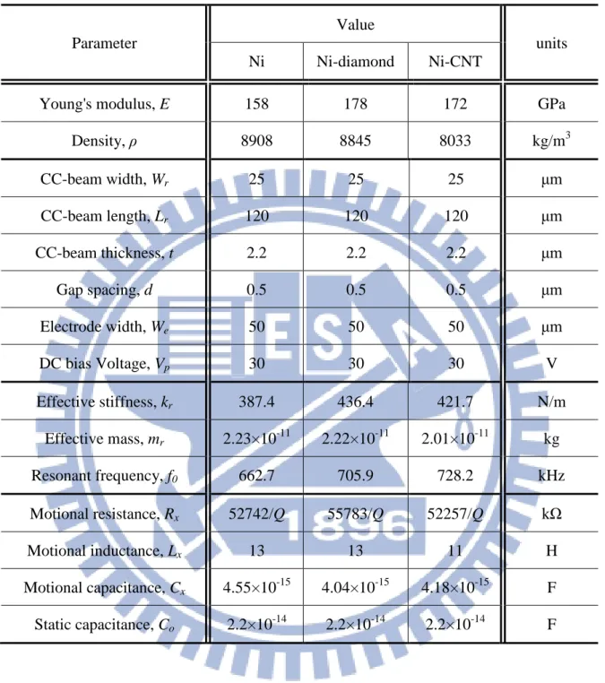
We and Wr are width of electrode and beam. Figure 2.2 depicts the design CC-beam resonator.
The relative dimensions are listed in Table 2.2. The resonant frequency of CC-beam resonator is set at 600-800 kHz. The gap spacing of CC-beam depends on the thickness of sacrificial layer which can be controlled in 500 nm. Therefore, the motional resistance can be reduced effectively.
2.2 Fabrication process of micromechanical resonator
The three-mask surface micromachining is adopted for Ni based micromechanical resonator fabrication. The usages of these three marks are defining the electrode, anchor, and structure of the resonator.
spin-coating and lithographically patterning on an electrical isolation layer, 500 nm thick SiO2,
followed by Ti/Ni layer (20/200 nm) deposition for device electrode fabrication on a silicon substrate. Sacrificial layer, like PR, is then coated, defined, and deposited with a sputtered Cu seed layer (200 nm) for following Ni-based composite electroplating. Before electroplating, thick PR like AZ-10XT is spun and patterned on the substrate as a mold (10 μm) where Ni-based film (6 μm) is electroplated to form microstructure. Micro-resonator fabrication is then finished after the removal of PR mold, Cu seed layer, and sacrificial layer by acetone, the mixture of CH3COOH and H2O2 (20:1), and PR stripper (Baker ALEG-370), respectively.
Figure 2.4 shows the process flow for the CC-beam resonator fabrication. The fabrication starts with thermal oxide (500nm) deposition as the isolation layer on a silicon wafer, followed by sputtering Ti/Ni (20/150nm) and Cu (500nm) as the electrode and sacrificial layer, respectively. Electrode and sacrificial layers are both patterned by lift-off process. Here, the electrode and sacrificial layers are also utilized as the seed layer for electroplating the anchors and suspended parts of the resonator. Before electroplating, a layer of thick photoresist, AZ10XT (>5μm), is spun and patterned as the mold where the Ni-based film is electroplated to form the resonator. At last, the fabrication is then finished after the removal of PR mold and Cu sacrificial layer by acetone and the mixture of NH4OH and H2O2 (4:1), respectively. Due to
good etching selectivity of the mixture of NH4OH and H2O2, the Cu sacrificial layer can be
removed completely without damaging the Ni-based structure.
The selectivity of the mixture of NH4OH and H2O2 for Ni and Cu is as good as
CH3COOH and H2O2. The PR sacrificial layer will be damaged while the Cu seed layer is
etching in the mixture of NH4OH and H2O2. Therefore, the mixture of CH3COOH and H2O2 is
2.3 The preparation of electrolytes
Sulfamate-based Ni electrolyte is chosen for electroplating due to low residual stress in film deposition. Ni film is DC (direct current) electroplated in the plating bath with the electrolyte comprising of nickel sulfamate of 400 g/L, boric acid of 40 g/L, nickel chloride of 3 g/L, and wetting agent (NPA, Atotech Inc.) of 5 g/L. On the other hand, either nano diamond particles with 125 nm in diameter or CNT with 10-20 (5-10) nm in outer (inner) diameters and 0.5-10 μm in length are added into the electrolyte for Ni-based nanocomposite electroplating. An aerating system as shown in Figure 2.5 is utilized to increase the diffusion of Ni ion and keep the nano-particles well suspended in the electrolyte. The plating bath with a pH level of 4.1~4.3 is put in a tank stored in a water immersion system where the temperature is kept at 35°C. Before being placed into the plating bath, the device substrate is first dipped in a 5% sulfate acid water solution for 10 sec and then rinsed in de-ionized water for 5 min.
Figure 2.1 The schematic of comb resonator and the excitation configuration.
Figure 2.3 Process flow of comb resonator.
Figure 2.5 Electroplating system. The nano particles are kept in well dispersion in electrolyte with aerating system.
Table 2.1 Design parameters and equivalent circuit value of comb resonator.
Parameter
Value
units
Ni Ni-diamond Ni-CNT
Young's modulus, E 158 178 172 GPa
Density, ρ 8908 8845 8033 kg/m3
Folded beam width, W 5 5 5 μm
Folded beam length, L 150 150 150 μm
Folded beam thickness, t 6 6 6 μm
Finger gap spacing, d 4 4 4 μm
Finger overlap length, Ld 40 40 40 μm
No. finger overlap, N 40 40 40 -
DC bias Voltage, Vp 60 60 60 V Effective stiffness, kr 70.2 79.1 76.4 N/m Effective mass, mr 2.99×10⁻⁹ 2.97×10⁻⁹ 2.69×10⁻⁹ kg Resonant frequency, f0 24.4 26.0 26.8 kHz Motional resistance, Rx 4.51×10⁸/Q 4.77×10⁸/Q 4.47×10⁸/Q kΩ Motional inductance, Lx 2.94×10⁶ 2.92×10⁶ 2.65×10⁶ H Motional capacitance, Cx 1.45×10⁻¹⁷ 1.28×10⁻¹⁷ 1.33×10⁻¹⁷ F Static capacitance, Co 2.1×10⁻¹⁴ 2.1×10⁻¹⁴ 2.1×10⁻¹⁴ F
Table 2.2 Design parameters and equivalent circuit value of CC-beam resonator.
Parameter
Value
units
Ni Ni-diamond Ni-CNT
Young's modulus, E 158 178 172 GPa
Density, ρ 8908 8845 8033 kg/m3 CC-beam width, Wr 25 25 25 μm CC-beam length, Lr 120 120 120 μm CC-beam thickness, t 2.2 2.2 2.2 μm Gap spacing, d 0.5 0.5 0.5 μm Electrode width, We 50 50 50 μm DC bias Voltage, Vp 30 30 30 V Effective stiffness, kr 387.4 436.4 421.7 N/m Effective mass, mr 2.23×10⁻¹¹ 2.22×10⁻¹¹ 2.01×10⁻¹¹ kg Resonant frequency, f0 662.7 705.9 728.2 kHz Motional resistance, Rx 52742/Q 55783/Q 52257/Q kΩ Motional inductance, Lx 13 13 11 H Motional capacitance, Cx 4.55×10⁻¹⁵ 4.04×10⁻¹⁵ 4.18×10⁻¹⁵ F Static capacitance, Co 2.2×10⁻¹⁴ 2.2×10⁻¹⁴ 2.2×10⁻¹⁴ F
Chapter 3 Process modification
3.1 Dispersion of nanoparticles
As shown in Figure 3.1, commercial nano diamond particles (Microdiamant AG Co., Ltd.) and CNTs (Seedchem Pty., Ltd.) prepared by a chemical vapor deposition method with 95% purity are adopt for nanocomposite plating. The average diameter of nano diamond particle is 125 nm. On the other hand, the inner and outer diameters and length of CNTs are in an average of 5-10 nm, 10-20 nm, and 0.5-200 μm respectively.
The size distribution of nano diamond particles provide by vendor is shown in Figure 3.2. The nano diamond particles are kept in the preservation solution with the known concentration. After adding into the electrolyte, the nano diamond particles can keep a good dispersion by the aerating system.
In Figure 3.1(b), the CNTs are in powder state. In order to fully adopt the unique properties of CNTs, it is necessary to disperse CNTs form each other in the electrolyte. Actually, the CNTs are often agglomerated in the solution by strong van der Waals force due to their nonpolarized surface characteristic and fiber shape. Many surface treatments have been developed to assist the dispersion of CNTs, and these methods can be classified into three general categories which are direct mixing, chemical surface modification, and third component assisted dispersion. Direct mixing is a method with mechanical force such as stirring or ultrasonication to separate CNTs from each other. It is one of the most convenient methods to achieve CNT dispersion. However, the dispersion quality is unsatisfactory [44]. Chemical surface modification of the CNTs starts with the treatment of CNTs with strong acids or other strong oxidizing agents and the functional groups are attached strongly on the nanotube walls, ends and defect sites of the CNTs. The functional groups help CNTs to expel each other.
Meanwhile, this treatment tends to disrupt and shorten the CNTs. The third method utilizes the third component, such as surfactants, which is coated on CNTs and helps CNTs dissolve into the solution. This method is very efficient without having any structural damage.
3.1.1 CNT surface modification
As aforementioned, we evaluate two kinds of CNTs treatments using H2SO4/H2O2 and
SDS water solutions which are commonly used for the dispersion of CNTs in water-based solutions [45, 46] and investigate the dispersion effects on the synthesis of electroplated Ni-CNTs nanocomposite for resonator fabrication.
Table 3.1 lists the recipes of the two kinds of surface treatment solutions which are covalent and non-covalent functionalization, respectively. Each solution is made for the treatment of 0.028 g CNTs whose inner and outer diameters and length are 5-10 nm, 10-20 nm, and 0.5-200 μm, respectively. After putting the CNTs in the treatment solutions, ultrasonication is performed for 120 min to ensure that the CNTs can separate from each other and fully disperse in the solutions.
The surface treatment of CNTs is shown in Figure 3.3. Firstly, the CNTs powders are added into the treatment solution. Then, ultrasonication is performed for 120 min to ensure that the CNTs can be separated from each other. Finally, the treated CNTs are spinning dry for morphology characterization by SEM. Figure 3.4 shows the dispersion characteristics of three kinds of treated CNTs after ultrasonication and quiescence. For a 120 min ultrasonication, both H2SO4/H2O2, SDS water solution, and DI water treated CNTs exhibit well dispersed
The CNTs on the Si wafer are shown in the following SEM images, Figure 3.5. The CNTs treated in DI water show a poor characteristic property in separation (Figure 3.5(a)). On the contrary, one treated by H2SO4/H2O2 and SDS water solution show the good dispersion.
The CNTs can be well separated from each other and the length of CNTs is in a range of hundreds nanometer to a few micrometers. The length of CNTs in the mixture is also measured by Dynamic Light Scatting (DLS) which is utilized for the detection of particle size in an aqueous solution. The measurement result indicates that the length of CNTs is in the range of 0.5 to 10 μm.
3.2 Gradient stress in Ni film
As-electroplated Ni film is usually accompanied with residual stress which would cause significant undesired structural deformation like beam curling and membrane winkling in suspended Ni-based MEMS devices. Figure 3.6 shows a Ni micromechanical resonator electroplated with the current density of 20 mA/cm2. In Figure 3.6(a), the 6 μm-thick as-released structure is warped down severely. When this comb structure plated with 3 μm-thick, as shown in (b), the structure curls more serious than one plated with 6 μm-thick. On the other hand, 16 μm-thick structure shows fully suspended as shown in Figure 3.6(c). It means that the stress would be compromised while the film thickness increasing. Actually, the demanded thickness of micromechanical resonator is 7 μm or less. Therefore, plating with high thickness (>16 μm) is not a reasonable solution for current approach. Ni-diamond or Ni-CNT nanocomposite comb resonator also exhibits similar behavior.
Because of the deformed structure, the Ni-based MEMS device must suffer either the problem of performance mismatch like capacitance mismatch [47] or the problem of performance degradation if the device structure must be made stiffer than the original design to overcome the warpage [48]. Since the incorporation of secondary phase would aggravate the
residual stress problem would become more severe in the Ni-based nanocomposite film [36], it is still a critical research topic to solve the curling phenomenon in electroplated Ni structures for future MEMS applications.
In fact, the warpage is mainly caused by the existence of stress gradient in the as-electroplated Ni film. Previously, the existence of stress gradient has been found and investigated in sputtered thin films, such as Cr, CrN and TiN [49-51]. The model of grain boundary shrinkage [52] were utilized to well explain the formation of stress gradient mainly resulted by the grain evolution in the sputtered thin films [49]. The mean stress (σavg) in the
sputtered thin film could be characterized using a power law, σavg~h -p, where h is film
thickness and p is the scaling exponential factor determined by the dynamics of the growth process [49]. According to TEM observation [49], the dependence can be attributed to the increase of the grain size over the thickness of the film where the number of grains per unit length (N) is also a function of the film thickness abided by the same power law, N~ h -p.
On the other hand, the stress gradient in the electroplated Ni film has not been investigated systemically yet. So far, only plating temperature has been identified as a key process parameter which can lead to the stress gradient relaxation of the film during plating because Ni atoms can migrate to relaxed positions [53]. Nevertheless, the Ni film electroplated at high temperature (over 70°C) usually accompanies with a high thermal stress level and the inclusion of nonmetallic atoms in the film which would affect the material elastic properties [54]. Since it has been reported that the mean tensile stress in electroplated Ni film would also obey the aforementioned power law and the stress level can be reduced by lowering current density [55], we, therefore, speculate that the stress gradient in electroplated Ni could be caused by the grain evolution when the film growth.
stress gradient of Ni and Ni-diamond nanocomposite films will be investigated and utilized as a process parameter for the modification and reduction of the stress gradient for MEMS fabrication. An optimal plating process with the lowest stress gradient is then derived and utilized to fabricate Ni-based micromechanical resonators. At final, the property enhancement of the nano-diamond-incorporated Ni composite film is verified by characterizing the frequency responses of the micromechanical resonators made of pure Ni and the nanocomposite films, respectively.
3.2.1 Gradient stress estimation
Figure 3.7 shows a micro-cantilever with two kinds of residual stress which are mean stress (σ0) and gradient stress (σ1), respectively. After releasing the sacrificial layer underneath
the cantilever as shown in Figure 3.7(b), the beam tends to be deformed owing to the stress. As shown in Figure 3.7(c), the stress gradient, Γ, can be approximately estimated in a linear distribution and expressed as follows [58, 59],
r E h h Δ Γ 1 1 2 1 − = = = ν σ σ (3.1) where r is the radius of beam curvature and E and ν are the Young’s modulus and Poisson ratio of Ni film, respectively. Thus, the surface profile and curvature of micro-cantilever will be measured by White-Light-Interferometer (FOGALE nanotech Inc.), as shown in Figure 3.8. Then, MATLAB is used to find the fitted curve and characterize its value. Young’s modulus of Ni and Ni nanocomposite are measured by nanoindenter (MTS systems Co., Nano-Indenter XP).
The perpendicular deformation can be resulted by the gradient stress and mean stress [59]. The mean and gradient stress would cause the beam tilting at its fixed end and the beam curling, respectively. Previously, the mean stress of Ni and Ni nanocomposite films has been
characterized by a long-short beam[60], as shown in Figure 3.9. The mean stress (σ0) applied
on the electroplated Ni beam can be calculated by the tip difference (Δ). According to the following equation [60], ∆ + − − = 4 3 2 1 2 2 2 1 1 0 3 2 S 2 n n L L n L L n E σ (3.2) where E is Young’s modulus. L1 and L2 are length of long beam and short beam, respectively.
S denotes the distance between center lines of the two beams. n1-n4 are the dimension
parameters given in reference [60]. The results indicated that mean stresses are small, which are 6.4, 7.4 and 10.3 MPa for Ni, Ni-diamond, and Ni-CNT films plated at 15.3 mA/cm2, respectively, and only result in a few nanometers deformation at the free end of the beam. Since the mean stress would be reduced when the current density reduction [55], it is reasonable to neglect the deformation caused by mean stress.
The measured dimensions cantilever beam and Yong’s modulus are shown in Table 3.2. Figure 3.10 shows the correlation between the plating current density versus the stress gradient of electroplated Ni and Ni-diamond nanocomposite films. It is inevitable to have a warped structure while the films are electroplated with high current density resulting in large stress gradient. For the same current density, the stress gradient of Ni-diamond nanocomposite film is about 1.5 times larger than that of Ni film. By lowering plating current density form 15.3 to 0.8 mA/cm2, the stress gradient can have 41% (from -5.46 to -3.23 MPa/μm) and 21% (from -7.13 to -5.65 MPa/μm) reduction in Ni and Ni-diamond nanocomposite films, respectively. Ni-CNT cantilever beam plated with 0.8 mA/cm2 reveals the stress gradient in -4.75 MPa/μm.
film plated with higher current density is comprised of finer grains. On the contrary, the average grain size of the Ni film plated with 0.8 mA/cm2 is larger than the previous one. As aforementioned, the grain structures in a sputtered polycrystalline film would gradually evolve from the nucleation/seed layer at a fine grain state to a texture structure with a preferred growth direction and the evolution would accompany with the variation of grain size and non-uniform residual stress distribution [49-51]. Figure 3.12 shows the grain size near the seed layer is about 50 nm. The Ni and Ni-diamond nanocomposite films plated with a lower current density would have the grain size distribution quickly saturated to a stable value, i.e. 170 nm and 150 nm in Figure 3.12(b) and (c), respectively. On the contrary, the grain size of the pure Ni one plated with a higher current density would increase with the height along the film thickness and no size saturation is observed as shown in Figure 3.12(a). Thus, for the case of electroplated Ni film, the stress gradient would form in the Ni film while the grain evolution takes place as and the film plated with higher current density will exhibit a larger stress gradient resulted by a thicker transition region, i.e. grain variance region, as shown in Figure 3.11(b). In addition, the nanocomposite film plated with 0.8 mA/cm2 has a grain size distribution similar to the Ni film even though nano diamond particles are incorporated.
The stress gradient reduction scheme in the electroplated Ni film can be further qualitatively illustrated as follows:
The origin of the stress can be illustrated by the model of grain boundary shrinkage [52], − = ν δ σ 1 ) ( ) ( E z G z (3.3) δ and G(z) are the shrinkage of the grain boundary and the grain size, respectively. Considering a transition region with the thickness of h, the stress gradient (Γ) of the film can be derived and expressed as follows by substituting Eq. 3.3 into Eq. 3.1,
) ( ) ( 1 1 h G z1 G z0 ΔG E h Δσ Γ ⋅ ⋅ − − = = ν δ (3.4) where z0 and z1 are the location at the bottom and top surface of the transition region,
respectively. In this expression, it shows the correlation of stress gradient with the grain size variation (∆G) and grain size (G(z)). Thus, electroplated with lower plating current density, the Ni film can have larger and uniformly distributed grain size which can effectively result in a lower stress gradient.
(a) (b)
Figure 3.1 Nano particles for nanocomposite electroplating: (a) nano diamond particles in the preservation solution and (b) carbon nanotubes (CNTs) powder.
(a) (b) (c) Figure 3.3 Process of CNTs surface treatments.
(a) (b)
(c) (d)
Figure 3.4 The CNTs in the treatment solution after quiescence (a) 0 min, (b) 120 min, (c) 160min, and (d) 200 min. From left to right: H2SO4/H2O2, SDS water solution, and DI water.
(a)
(b)
(c)
Figure 3.5 The CNTs treated by (a) DI water, (b) H2SO4/H2O2, and (c) SDS water solution and
(a)
(b)
(c)
(a) (b)
(c)
Figure 3.7 Micro-cantilever beam (a) before and (b) after release. (c) The stress distribution can be expressed by the mean stress (σ0) and gradient stress (σ1)
(a) (b)
(c)
Figure 3.8 (a) The surface profile of cantilever beams are characterized by White-Light-Interferometer. (b) The cutting curve is extracted from the surface profile. (c) MATLAB is used to find the fitted curve and its value.
Figure 3.10 The stress gradient of Ni, Ni-diamond, and Ni-CNT nanocomposite films under different current density.
(a) (b)
Figure 3.11 (a) FIB cross sectional images of Ni films electroplated at 15.3 mA/cm2 and 0.8 mA/cm2 and Ni-diamond at 0.8 mA/cm2 (from left to right). (b) Model of grain evolution of electroplated Ni.
(a)
(b)
(c)
Figure 3.12 The grain size versus height: Ni plated at (a) 15.3 mA/cm2 and (b) 0.8 mA/cm2. (c) Ni-diamond nanocomposite plated at 0.8 mA/cm2.
Table 3.1 Dispersion treatments of CNTs
Covalent functionalization Non-covalent functionalization
H2SO4, 15mL
H2O2, 5mL
Sodium dodecyl sulfate (SDS), 0.04g De-ionized (DI) water, 20mL
Table 3.2 The measured material properties and dimensions of the cantilever beams made of Ni, Ni-diamond, and Ni-CNT nanocomposite.
Current density Young’s modulus Thickness Radius of curvature
Units mA/cm2 GPa μm μm
Ni 15.3 141 5.34 40230 11.5 144 5.85 43853 7.7 148 5.79 47092 3.8 152 6.15 53743 0.8 154 6.54 65343 Ni-diamond 15.3 186 5.84 40681 11.5 191 6.07 42279 7.7 197 5.54 43827 3.8 202 6.16 44999 0.8 206 6.3 52724 Ni-CNT 0.8 173 7.05 93249
Chapter 4 Characterization of micromechanical resonator
4.1 Measurement setup
We measure the frequency responses of micromechanical resonators. According to the frequency responses, it is easy to obtain the resonant frequency and Q. Resonant frequency is the frequency with maximum displacement. On the other hand, Q can be calculated by the following expression: f f Q ∆ = 0 (4.1) where f0and Δf are resonant frequency and half power bandwidth (or 3db bandwidth). Optical
measurement is adopted for the preliminary frequency response (displacement versus frequency) tests of resonators. After optical measurement, electrical measurement is taken for output electrical signal measurement.
4.1.1 Optical measurement
Figure 4.1 shows the in plane motion measurement setup where MEMS Motion Analyzer (Etec Inc., MMA G2) is used for characterizing the frequency response of resonators as shown in Figure 4.1(a). The MMA combines microscopy and stroboscopic illumination to analyze the periodical motions of microstructures. The resonator is driven by the function generator of the MMA. The Vbias (from 60 to 120 V) and Vi (from 2 to 10 V) are applied on the resonating
comb resonator with different vibrating amplitude can be obtained.
Laser Doppler Vibrometer (Ono Sokki Co., Ltd., LV-1716) is used to measure the out of plane displacement. The measured out plane displacement will be converted into voltage form and outputted by LDV. As shown in Figure 4.2, the CC-beam resonator is driven by Vi, AC
voltage supplied by network analyzer, and Vbias, DC voltage supplied by voltage source.
During measurement, network analyzer will provide AC voltage signal output with varied frequency and reads the input signal provided by LDV. The read signal can be converted into displacement and the frequency response of CC-beam resonator can be obtained.
4.1.2 Electrical measurement
Figure 4.3 presents the CC-beam resonator with a typical driving and electrical sensing setup. The resonator consists of a movable flexural beam clamped at both ends and a driving electrode underneath the beam. DC bias voltage (Vbias) is applied to the resonator, while an
AC excitation voltage (Vi) is applied to the electrode. When the frequency of Vi matches the
resonant frequency of the resonant beam, the resonator begins to vibrate to form a time-varying capacitor. This time-varying capacitor biased with the DC voltage could generate an output current (io). The data of frequency characteristic is collected using a
network analyzer (Agilent Technologies Inc., E5071C) with active probe (Agilent Technologies Inc., 41800A) for matching impedance between input port of network analyzer and resonator. The CC-beam resonator is placed into a vacuum chamber and the measurement is performed at the pressure under 0.5 mTorr.
4.2 Characterization of micromechanical resonator
4.2.1 Diamond and CNT incorporation
According to the pervious test, the dimensions of nano particles can be summarized and shown in Table 4.1. The nano diamond particles and CNTs incorporation of the nanocomposite can be verified by the SEM photos taken at the top surface of plated films. Basically, the nanocomposite synthesis is to electroplate the Ni matrix in the solution with well-dispersed nano particles. The bath with an aerating system could ensure that the particles are uniformly attached to the as-plated Ni film and then engulfed into a metal matrix during the plating processing. In the previous investigation, the nano diamond particles were found to be incorporated randomly in the matrix [40]. The SEM shown in Figure 4.4(a) image also shows the top surface of nanocomposite film where nano diamond particles are well distributed in the Ni-diamond nanocomposite film. On the other hand, the CNTs incorporation is shown in Figure 4.4(b). At the top surface, CNTs partly engulf into Ni film and reveal a random distribution. By the way, no void is observed in the SEM photos.
The amount of nano particle incorporated in the Ni film can be characterized by the elemental analyzer (Heraeus, varioIII-NCH). From the detected carbon concentration, it is found that the volume percentages of incorporated nano-diamond or CNTs are proportion to the nano particle concentrations in the Ni plating bath, as shown in Figure 4.5. With nano diamond particle concentration of 2 g/L, the volume percentage is 0.44%. The volume percentage is 13.9% with CNTs concentration of 1 g/L.
and Ni-CNT resonators (Figure 4.6(b)) electroplated at 0.8 mA/cm2. It indicates that the springs still have a little downward warpage but they have been fully suspended to support the whole micro-resonator structures.
Figure 4.7 shows the frequency response of the comb resonators made of Ni and Ni-diamond, and Ni-CNT indicating the related resonant frequencies are 22.55, 25.75, and 24.45 kHz, respectively. About 14% and 8% resonant frequency enhancement can be realized in the Ni-diamond and Ni-CNT nanocomposite micro-resonators where the composite film is electroplated in a Ni electrolyte with 2 g/L nano-diamond and 0.028 g/L CNTs, respectively. Meanwhile, the measured response also shows the nanocomposite comb resonators have higher quality factors than that of Ni at atmospheric pressure. The measured quality factors of Ni, Ni-diamond, and Ni-CNT comb resonators are 124, 201, and 217, respectively. The measured dimensions and resonant frequencies are summarized in Table 4.2.
According to rule of mixture [61, 62], the Young’s modulus of two-phase composite can be estimated by the upper and lower bound expressions as follows, respectively,
D D m m upper composite E V E V E , = + (4.2) and m D D m D m lower composite V E V E E E E + = , (4.3) where the Em, ED, Vm and VD are Young’s moduli and volume fractions of the matrix and
secondary phase, respectively. Based on the measured Young’s modulus, the mechanical property of the Ni nanocomposite film with the volume ratio of 0.46% nano-diamonds can only have 2.3% and 0.3% Young’s modulus enhancements estimated by the upper and lower bounds, respectively. Thus, according to the upper bound of the estimated Young’s modulus, it indicates only 1.5% resonant frequency increase can be achieved. In comparison of the measured resonant frequencies of the comb resonators, nano diamond incorporation can bring more enhancement than that estimated by the upper bound. The frequency enhancement can be
attributed to two possible factors which can result in the Young’s modulus increase of the nanocomposite film. According to the previous study [63], it was found that the more compressive-stressed film will come with a higher Young’s modulus. Since the nano diamond incorporation would cause Ni film with more compressive stress [36], it may cause the increase of Young’s modulus of Ni part of nanocomposite so that the Young’s modulus of the nanocomposite can be enhanced with a value larger than the one estimated by the rule of mixture.
Figure 4.8 shows the frequency-response spectrum of the as-fabricated Ni and Ni-CNT nanocomposite comb resonators. The resonant frequency of the SDS treated Ni-CNT nanocomposite resonator is 30.65 kHz which is higher than the one made of pure Ni and the H2SO4/H2O2 mixture treated Ni-CNT nanocomposite which are 29.35 kHz and 30.35 kHz
respectively. The measured dimensions and resonant frequencies are summarized in Table 4.3. Figure 4.9 shows SEM micrographs of as-fabricated Ni-CNT comb resonators where the CNTs are treated by H2SO4/H2O2 and SDS solutions, respectively. In addition, the Energy Dispersive Spectroscopy (EDS) analyses on the resonator springs verify the incorporation of CNTs and further indicate that the embedded CNTs in the SDS treated nancomposite is higher than that treated by H2SO4/H2O2 solution because SDS treated nanocomposite has a higher
carbon intensity than that of the nanocomposite treated by H2SO4/H2O2.
4.2.3 Performance measurement of clamped-clamped beam resonators
Figure 4.10(a) and (b) show the SEM images for Ni and Ni-CNT CC-beams, respectively. The measured thickness of structure and sacrificial layer are 2.27 μm and 531 nm for NiFigure 4.11 presents the frequency responses of Ni, Ni-diamond, and Ni-CNT CC-beam resonators at 0.2 mTorr. The measured data is summarized in Table 4.4. It shows resonant frequencies (f0) of 498.75, 725.47, and 634.72 kHz for the Ni and Ni-CNT CC-beam
resonators, respectively, designed with the same dimensions. About 45% and 27% frequency enhancement can be realized and attributed to the incorporation of nano diamond particles and CNTs. In addition, it can be found that the electrical sensing results are different from that of the LDV measurement. This frequency reduction is caused by the introduction of electrical stiffness (ke) related to the interaction of the electric field between the resonator and drive
electrode, and hence, the effect would lower the effective spring stiffness as follows [64]:
r r e bias r r e r m g W W V k m k k f ( / ) 2 1 2 1 0 3 2 0 ε π π − = − = (4.4) where kr and mr are the mechanical spring constant and mass of the resonator, respectively.
From (4.4), the electrical spring constants of the Ni and Ni-CNT resonators are calculated as 118.3, 113.2, 140.8 N/m, so the calculated resonant frequencies of the resonators applied with
Vbias are 504, 701, and 639 kHz, which are close to the aforementioned measurements. The
measured Q values of the Ni, Ni-diamond, and Ni-CNT CC-beam resonators are 781, 612, and 760, respectively, indicating that nano particle incorporations did not cause the Q degradation.
According to the previous research work [23], the electroplated Ni CC-beam resonator indicated the quality factor in 576. This level is lower than poly-Si CC-beam resonators [10]. The anchor loss is to dominate the Q’s of poly-Si CC-beam resonator and it might also applicable in the Ni-based case, since the attachment of Ni resonators to the substrate at their anchors is not as sturdy as the polysilicon counterparts. The anchor loss becomes more severe in the Ni-based case. Poor adhesion caused by the stress of the plated film between the structure and the substrate could result in a weak anchor that ultimately dissipates more energy during vibration. Nevertheless, it is difficult to make a solid conclusion regarding loss
mechanisms based on Ni-based CC-beam resonator measurements and further Q investigation related to material quality is underway by fabricating free-free-beam-typed resonators.
4.2.4 Temperature coefficient of frequency
Resonant frequency variation over temperature is defined as temperature coefficient of frequency (TCF) which is expressed as:
T f f TCF ∂ ∂ = 0 0 1 (4.5)
T and f0 are the operational temperature and resonant frequency. The frequency shift with
changing the temperature is shown in Figure 4.12. The slopes of curves are the TCFs. For Ni, Ni-diamond, and Ni-CNT CC-beam resonators, TCFs are -5.49×10⁻³, -3.47×10⁻³, and -4.58× 10⁻³ /°C respectively. It is found that Ni-diamond and Ni-CNT resonator has lower TCF than Ni one.
Actually, the value of TCF depends on thermal stress, temperature coefficient of Young’s modulus, and thermal expansion coefficient. For the CC-beam design, the TCF can be expressed in terms of these parameters [65],
2 2 1 σ α σ β β ∂ + + ∂ ∂ ∂ = TCE T TCF (4.6)
β and σ are the mode constant and axial stress of CC-beam. TCE and α are the temperature
coefficient of Young’s modulus and thermal expansion coefficient of material. TCE of Ni was investigated about -7.65×10⁻⁴ /°C [66]. Thermal expansion coefficients of Ni, Ni-diamond, and Ni-CNT are 2.3×10⁻⁵, 5×10⁻⁵, and 3.5×10⁻⁵, respectively [38, 40]. Comparing with our
Ni-based structure. The compressive stress would lower the resonant frequency.
4.2.5 Power handling capability of CC-beam resonator
Through coupling, micromechanical resonators can serve as filters [67-69]. For the demand of future systems, increasing power levels of filter is the simplest way to boost system range and capability [70]. Therefore, it is important for micromechanical resonator with high power handling capability. For a capacitivly-transduced resonators, the maximum power handling is defined by the maximum output current Iomax and motional impedance Rm,
2 max max
o o m
P =I ×R
(4.7) By manuplating the above equation, the theoretical maximum power handling can be expressed by 1st and 3rd order equivalent stiffness (k1 and k3) of the resonator [71, 72]:
2 3 2 1 0 max 1.16 Q k k Po ≤ ω (4.8)
ω0 and Q radian resonant frequency and quality factor of resonator, respectively. For
capacitivly-transduced resonators with high dc-bias voltages, the 1st and 3rd order equivalent stiffness can be approximated as
(
f) ( )
m y k k1= re = 2π0 2 r (4.9) and 2 5 0 0 3 3 2 3 p e V d A k k = = ε (4.10) where ke3 denotes the 3rd-order electrical stiffness. We can find that for two resonators withsimilar dimension, quality factor, and 3rd-order electrical stiffness, the resonator who has higher mechanical stiffness kre and resonant frequency would get better power handling
capabilities.
![Figure 1.1 Time and frequency components in GSM handset [1].](https://thumb-ap.123doks.com/thumbv2/9libinfo/8755138.206724/20.892.137.801.112.975/figure-time-frequency-components-gsm-handset.webp)
![Figure 1.5 Energy loss mechanisms of micromechanical resonator and their dependence on frequency [8]](https://thumb-ap.123doks.com/thumbv2/9libinfo/8755138.206724/22.892.128.788.134.966/figure-energy-loss-mechanisms-micromechanical-resonator-dependence-frequency.webp)
![Table 1.1 Material properties of popular MEMS structural materials [31].](https://thumb-ap.123doks.com/thumbv2/9libinfo/8755138.206724/24.892.150.796.187.915/table-material-properties-popular-mems-structural-materials.webp)