國立臺灣大學電機資訊學院電信工程學研究所 碩士論文
Graduate Institute of Communication Engineering College of Electrical Engineering and Computer Science
National Taiwan University Master Thesis
以電晶體負阻抗轉換器實現非福斯特電路
Non-Foster Circuits Realized by Transistor Negative-Impedance Converters
吳蕙心
Skye Huihsin Wu
指導教授:陳士元 博士 Advisor: Shih-Yuan Chen, Ph.D.
中華民國 105 年 1 月 Jan, 2016
i
摘要
本論文旨在探討以電晶體負阻抗轉換器實現非福斯特電路於特高頻(UHF)之 可行性。目前在此頻段少有實作案例,本文藉由分析電路中的非理想效應,探討 可能的阻礙,並且利用這些分析,嘗試設計並實作可工作於特高頻的負電感與負 電容。
關鍵字:非福斯特電路、負阻抗轉換器
ii
Abstract
The feasibility of realizing a non-Foster circuit at UHF (ultra high frequency) by transistor negative-impedance converters is discussed in this work. There are only a very few negative-impedance converters built for this frequency band, and the possible difficulties that may be encountered in the design processes are discussed by analyzing the non-ideal effects in the circuits. In addition, these analyses are used in the attempt to design and to build negative capacitors and negative inductors that can operate at UHF.
Index Terms — Non-Foster Circuits, Negative Impedance Converters
iii
Contents
摘要 ... i
Abstract ... ii
Contents ... iii
List of Figures ... v
List of Tables ... viii
Chapter 1 Introduction ... 1
1.1 Non-Foster Circuits ... 1
1.2 The Cross-coupled Pair as a Negative Impedance Converter ... 1
1.3 Chapter Outline ... 3
Chapter 2 Linvill’s Transistor Negative-Impedance Converters ... 4
2.1 The Original Design by Linvill ... 4
2.2 Higher-Frequency Model of Linvill’s Transistor NIC ... 8
2.3 Input Impedance of NIC with Resistive Load ... 16
2.4 Input Impedance of NIC with Reactive Load ... 19
Chapter 3 Design of the NIC Realized by Practical Circuit Components ... 25
3.1 Practical RF Transistors ... 26
3.1.1 Package of RF Transistors ... 26
iv
3.1.2 Intrinsic Property of RF Transistors ... 32
3.1.3 The Model of VMMK-1218 ... 32
3.2 Practical Inductors and Capacitors ... 35
3.2.1 Selection of the NIC Load ... 35
3.2.2 Selection of DC blocking capacitors ... 36
3.2.3 Selection of RF chokes ... 36
3.3 NICs consist of practical circuit components ... 38
Chapter 4 Implementation of the NIC ... 43
4.1 Simulation of the prototype NIC circuit ... 43
4.2 Fabrication of the prototype NIC circuit ... 47
4.3 Conclusion ... 47
4.4 Future works ... 48
Reference ... 50
v
List of Figures
Figure 1.1 NICs realized by XCPs ... 2
Figure 2.1 Linvill’s NIC ... 5
Figure 2.2 Equivalent circuit of Linvill’s NIC ... 6
Figure 2.3 Input impedance of Linvill’s NIC ... 7
Figure 2.4 Higher-frequency small signal model of a field-effect transistor ... 8
Figure 2.5 Higher-frequency model of the NIC ... 10
Figure 2.6 Small signal model of the transistor VMMK-1218 ... 14
Figure 2.7 Input impedance of the NIC loaded with a 50Ω resistor ... 18
Figure 2.8 Frequency response of ideal −3-nH inductor (dash line) and the NIC loaded with 3-nH inductor. ... 22
Figure 2.9 Frequency response of the NIC loaded with ideal 3-nH inductor (with the internal capacitance of the transistors ignored) and ideal −3-nH inductor (dash line). ... 23
Figure 3.1 Package of Avago ATF-55143 ... 28
Figure 3.2 Simple higher-frequency FET model with parasitic inductors at the terminals ... 28 Figure 3.3 Input impedance of the NIC loaded with 3-nH inductor (thicker
vi
line−transistor with parasitic inductance) ... 29
Figure 3.4 Small signal model of a transistor housed in a WSP ... 30
Figure 3.5 Core of the NIC ... 31
Figure 3.6 0402 WSP of a transistor ... 31
Figure 3.7 Simulation of the two transistor small-signal models ... 33
Figure 3.8 S-parameters of the two transistor small-signal models (circle line: full model) ... 33
Figure 3.9 Input impedance of the NIC predicted by the simple and full circuit model 34 Figure 3.10 Frequency response of practical 10pF/20nH capacitor/inductor [6] ... 35
Figure 3.11 Input impedance of the 1-μF capacitor (circle line: reactance) ... 40
Figure 3.12 Impedance of the 560-nH inductor (circle line: reactance) ... 40
Figure 3.13 Impedance of the 120-nH inductor (circle line: reactance) ... 40
Figure 3.14 NIC consists of practical circuit components... 41
Figure 3.15 Impedance of NIC loaded with 1-pF capacitor compared with ideal −1.2 pF capacitor (circle line: ideal −1.2 pF capacitor) ... 41
Figure 3.16 Impedance of NIC loaded with 2.9-nH inductor compared with ideal −2.9 nH inductor (circle line: ideal −2.9 nH inductor) ... 42
Figure 3.17 Impedance of the 1-pF load and an ideal 1-pF capacitor (circle line: ideal 1-pF capacitor) ... 42
vii
Figure 3.18 Impedance of the 2.9-nH load and an ideal 2.6-nH inductor (circle line:
ideal 2.6-nH inductor) ... 42
Figure 4.1 Geometry of the prototype NIC ... 44
Figure 4.2 Schematic design of the prototype NIC used in the simulation ... 44
Figure 4.3 Core of the prototype NIC ... 45
Figure 4.4 Simulated S-parameters of the 2-port NIC network ... 45
Figure 4.5 Schematic design for simulating the impedance between the sources of the two transistors ... 46
Figure 4.6 Simulated impedance between the sources of the two transistors (circle line: without the effects of the transmission lines and the substrate) ... 46
Figure 4.7 Photograph of the prototype NIC ... 47
viii
List of Tables
Table 2.1 ... 17
Table 2.2 ... 18
Table 2.3 ... 20
Table 2.4 ... 21
1
Chapter 1
Introduction
1.1 Non-Foster Circuits
Foster’s reactance theorem states that the slope of the driving-point impedance of a lossless one-port versus frequency is positive. However, by using active devices, it is possible to realize elements that has negative reactance-versus-frequency slope. These elements are called “non-Foster circuit”, which are typically negative capacitors and negative inductors or their combinations realized by the negative-impedance converters [1].
1.2 The Cross-coupled Pair as a Negative Impedance Converter
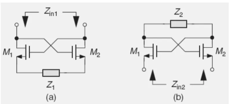
The negative impedance converters (NIC) realized by the cross-couple pairs (XCP) are shown in Figure 1.1. If the XCP operates in equilibrium (with its drain voltages of the two transistors equal to each other), it behaves in the small-signal regime. The input
2
impedance of the XCP in the Figure 1.1 can be derived by small-signal analysis.
Assuming the transistors are ideal, the XCP produces an impedance of Zin1=−Z1−2/gm between the drains or Zin2=−Z2+2/gm between the sources [2].
Figure 1.1 NICs realized by XCPs
The first practical transistor XCP NIC was designed and tested by Linvill [3] in 1954, which will be reviewed in the next chapter. It is originally designed as a negative resistance operating in several tens of KHz. Since then, many attempts are made to build XCP NICs for various operating frequencies. Most of these NICs are designed to
operate at high frequency (HF) or very high frequency (VHF).
XCP NIC is difficult to achieve at higher frequencies for two reasons. First, the effects of internal capacitances of transistors and other circuit parasitic elements become significant at higher frequencies, and thus affect the performance of the NIC. Second, the XCP NIC can form an oscillator with nearby circuit parasitic elements and become unstable. In fact, XCPs are often used in oscillator designs to provide the needed
3
positive-feedback.
1.3 Chapter Outline
The feasibility of XCP NICs operating at ultra high frequency (UHF) is discussed in this work. Since the parasitic effects in the NIC circuit become complicated at UHF and make the performance of NIC difficult to predict, parasitic effects from different parts of the NIC are discussed separately. In chapter 2, the impacts of the transistors’
internal capacitances on the NIC are discussed. A higher-frequency model of the NIC is proposed, and it is used to explain some behaviors of the NIC at UHF. In chapter 3, the non-ideal behaviors of the commercial surface-mount devices used in the NIC are discussed, and a new NIC design are proposed and simulated by taking these effects into account. In chapter 4, the effects of the transmission lines and junctions in the NIC are discussed, and a NIC prototype is simulated and built. The conclusion and future work are also addressed in chapter 4.
4
Chapter 2
Linvill’s Transistor Negative-Impedance Converters
In this chapter, the original negative-impedance converter (NIC) designed by Linvill back in 1952 is reviewed first. Then, in order to discuss the behavior of the NIC at UHF, a new circuit model effective at several GHz is proposed by the author. Mathematical expressions of the input impedance of a loaded NIC are derived from the new circuit model, and moreover, these expressions are used to discuss the potential and limitation of the NIC circuit.
2.1 The Original Design by Linvill
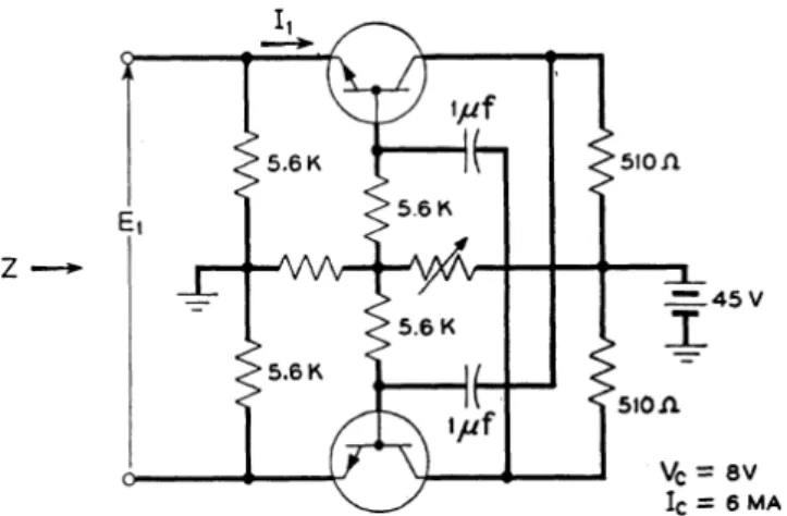
Linvill’s transistor negative impedance converter (NIC) shown in Figure 2.1 is designed for several tens of KHz. It is mainly composed of two cross-coupled bipolar junction transistors (BJTs) with the loads connected between the collectors. The 510-Ω resistors are used as loads. The 1-μF capacitors are used to couple the ac signal and to
5
block the dc bias currents. Following is a simple explanation of this configuration proposed by Linvill. First, almost all the current goes through the upper transistor and then to the loads, building a voltage on that, and finally goes out of the emitter of the lower transistor. Meanwhile, the voltage on the loads is cross-coupled by the 1-μF capacitors to the bases of the transistors. This inverted voltage then reaches the input terminals since the impedances between the emitters and the bases are small. Therefore, the negative of load impedance shows in the input terminals because of the positive-polarity current and the negative-polarity voltage compared with the loads.
Figure 2.1 Linvill’s NIC
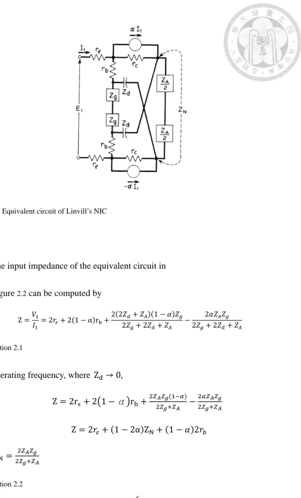
6 Figure 2.2 Equivalent circuit of Linvill’s NIC
The input impedance of the equivalent circuit in
Figure 2.2 can be computed by
Z = = 2 + 2(1 − α)r +2(2 + )(1 − )
2 + 2 + − 2
2 + 2 +
Equation 2.1
at the operating frequency, where Z → 0,
Z = 2r + 2 1 − α r + ( )−
Z = 2 + (1 − 2α)Z + (1 − )2 where Z =
Equation 2.2
7
The above expression is reached with the assumption that Z /r is negligible. The assumption is valid for the average NIC of that time, in which the load ZA is in the order of KΩ and r is in the order of MΩ. The frequency response of the transistor is modeled
by the change of α according to the relationship α = /
Equation 2.3
where is the cut-off frequency of the transistor.
The variation of the input impedance of the NIC with respect to frequency can be seen in Figure 2.3.
Figure 2.3 Input impedance of Linvill’s NIC
8
2.2 Higher-Frequency Model of Linvill’s Transistor NIC
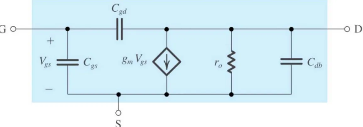
In the previous section, the model and the performance of the original Linvill’s transistor NIC is introduced. However, for nowadays uses, a higher operating frequency and a wider bandwidth are desired, thus a higher-frequency model that can characterize the structure in a larger frequency range is needed. To study the feasibility and limitation of Linvill’s NIC circuit topology, a hybrid-π higher-frequency small signal model for field-effect transistors in Figure 2.4 functioning as a good approximation up to several GHz is used in the following discussion. The field-effect transistors (FET) are adopted instead of bipolar junction transistors (BJT) because the model of FETs is simpler than that of BJTs. In addition, the voltage-controlled characteristic of FETs may also simplify the testing process.
Figure 2.4 Higher-frequency small signal model of a field-effect transistor
9
Although the model is very simple, it can be used to explain some non-ideal characteristics and practical issues of Linvill’s transistor NIC, including the parasitic input reactance/resistance, the bandwidth in which the negative impedance (non-Foster) is preserved between the input terminals, and the potential non-stability at higher band.
This pi-model of a field effect transistor (FET) includes the gate-source, gate-drain, and drain-source capacitors , , , and the output resistor r .
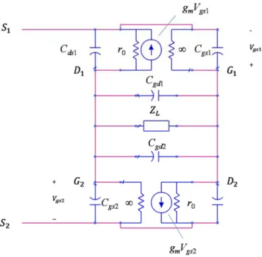
The transistor models in the Linvill’s circuit analysis are replaced by the above model, and a new equivalent circuit is obtained and shown in Figure 2.5. The load impedance is denoted by ZL, where = + . The output resistors exist between the drain and source of the transistor are denoted by = = 1/ . For simplicity, the coupling capacitors on the cross-transistor-coupling path are omitted. Their impacts will be discussed in the next chapter.
The input impedance expression is:
G Z − g Z + sZ C + C + 4C + 2
G + g + s C + C + 2s C + + + 2sZ G (C + ) + 2sZ g C
Equation 2.4
where s denotes the complex frequency.
10
A direct observation of the input impedance expression reveals that if the transconductance gm dominates and the NIC is operating at lower frequencies, where the circuit was originally designed for, the input impedance will be −ZL. However, for the GHz band, the transconductance of the transistors is smaller than 1, and the terms containing frequency and the parasitic capacitors of the transistor become significant, thus the frequency response of the input impedance is more complicated. In the following sections, this expression will be used to discuss the parasitic input reactance/resistance, the bandwidth in which the negative impedance (non-Foster) is preserved between the input terminals, and the potential non-stability of the NIC at higher band.
Figure 2.5 Higher-frequency model of the NIC
11
By expanding the input impedance expression and substituting the complex frequency s with j2πf, the resistive and reactive parts of the input impedance are:
R
={( − ) + (2 )( + 4 + ) − 2} 2 + {(− + ) + (2 )( + 4 + )} 1
1 + 2
X
= − (− + ) + (2 )( + 4 + ) 2 − ( − ) + (2 ) + 4 + − 2 1
1 + 2
A1 = 2πf C + C − 8π + + + 4 ( + + )
A2 = 8π + + − − + 4 ( + + )
Equation 2.5
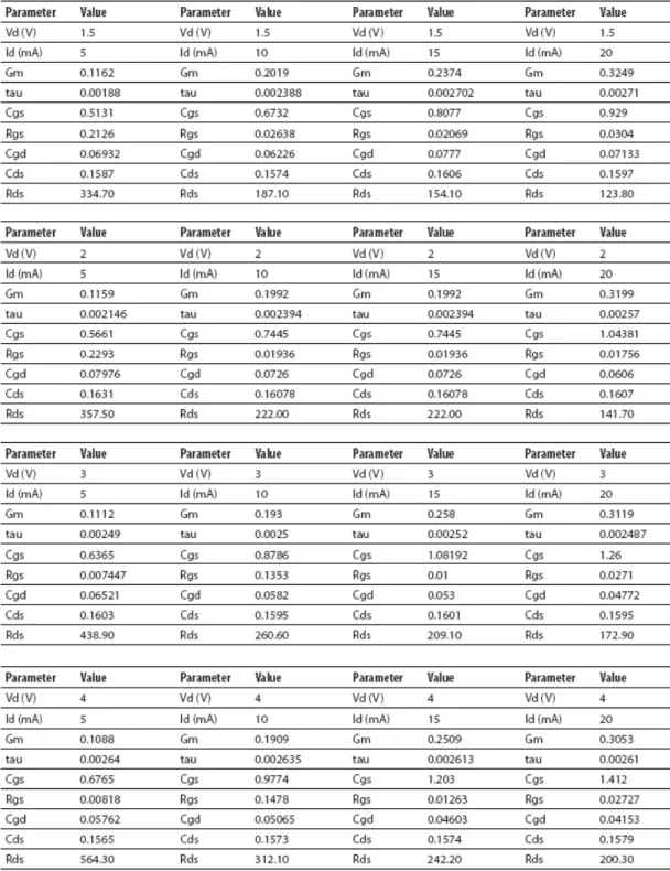
For the two types of small/medium power FETs commonly used in the GHz designs, namely the high-electron-mobility transistor (HEMT, also known as heterostructure FET, HFET) and metal-semiconductor field-effect transistor (MESFET), Cgs and Cds are in the order of 10 F, and Cgd is in the order of 10 F. gm is in the order of 10 or 10 S. The value of these parameters varies with the bias conditions and the size of the transistors. The choice of the transistors based on these parameters will be discussed in
12
the next chapter. The transistor used here for demonstration is VMMK-1218 from Avago Technology. Its parameters for a series of bias conditions are shown in Figure 2.6. It should be noticed that the small signal model of the transistor suggested by Avago is more complicated than that in Figure 2.4. The difference between these two models will be discussed in the next chapter. For now, the simple model of transistor in Figure 2.4 is used, in which the values of parasitic capacitance , , is determined by the corresponding values in Figure 2.6.
13
14
Figure 2.6 Small signal model of the transistor VMMK-1218
15
If the bias condition of the transistors is = 4 , = 5 , the numeric expression of the input impedance calculated by Equation 2.5 is:
, , =(0.107 + 0.00668 − 2) 2 − (0.107 − 0.00668 ) 1
1 + 2
, , =(0.107 − 0.00668 ) 2 + (0.107 + 0.00668 − 2) 1
1 + 2
1 = 0.00523 + 9.51 × 10 − 1.21 × 10
2 = 1.21 × 10 + 9.51 × 10 − 0.111
where ff denotes the frequency in GHz.
Equation 2.6
Two special configurations will be discussed in the following two sections. First, for a purely resistive load = , the expression of the input impedance is derived. In contrast, for a purely reactive load = , similar analysis is conducted. These impedance expressions will be used to discuss the parasitic input reactance/resistance of the NIC. The bandwidth in which the negative impedance (non-Foster impedance) is preserved between the input terminals and the potential non-stability of Linvill NIC at higher band will also be analyzed, whose effects can be seen clearly in the impedance formulas.
16
2.3 Input Impedance of NIC with Resistive Load
Based on Equation 2.6, the input resistance of the NIC with a resistive load can be calculated as:
= − . + . + 1.07 × 10 + 1.93 × 10
. + 2.74 × 10 − 1.69 × 10 + 9.04 × 10 + 1.46 × 10
Equation 2.7
Clearly, the “negative resistance” is degraded mainly by the second term in the numerator, while the third and fourth terms are negligible at lower frequencies. For the denominator, only the first term is dominant at lower frequencies. As a result, the magnitude of the negative resistance at lower frequencies would be about 20 Ω smaller than expected.
The input reactance is also calculated. For a purely resistive load, a negative input resistance is expected at the operating frequency, thus the reactance observed at the input port can also be seen as “parasitic” input reactance:
=− 0.0105 + 0.00111 + 1.02 × 10 − 8.12 × 10 (−0.111 + 1.21 × 10 ) + (0.00523 + 9.51 × 10 )
= − . + . + . × − 8.12 × 10
. + 2.74 × 10 − 1.69 × 10 + 9.04 × 10 + 1.46 × 10
Equation 2.8
17
Assuming that is in the order of 10 and the NIC is operating at several GHz, the magnitude of the parasitic input reactance could be several Ω or several tens of Ω.
As a reference, a simple calculation is done under the assumption that RL = 50Ω, ff = 1GHz & 5GHz, and the magnitude of each significant terms are tabulated in Table 2.1 and Table 2.2. It can be seen that the NIC functions more like a negative resistor at 1 GHz than at 5 GHz because the negative resistance is about −30 Ω, and the parasitic reactance is only about 6 Ω. At 5 GHz, the absolute value of the input reactance is larger than that of input resistance, and thus the circuit is no longer a good NIC.
term Magnitude at 1 GHz
−0.0105 ff −0.0105
0.00111 RL ff 0.0555
1.02 × 10 0.0255
Rin by Equation 2.7 −29.9538
Xin by Equation 2.7 5.7596
Table 2.1
18
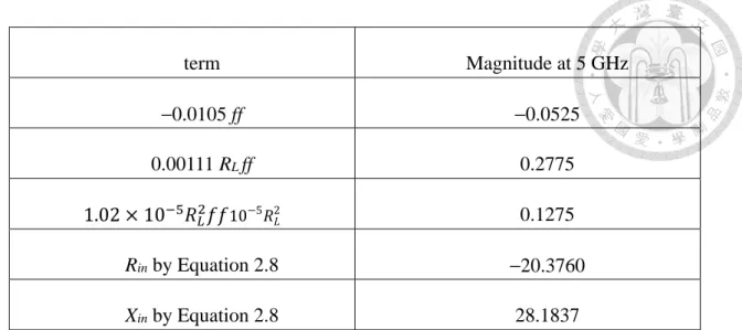
term Magnitude at 5 GHz
−0.0105 ff −0.0525
0.00111 RL ff 0.2775
1.02 × 10 10−5 2 0.1275
Rin by Equation 2.8 −20.3760
Xin by Equation 2.8 28.1837
Table 2.2
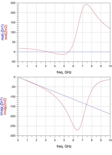
The input impedance response of the NIC loaded with Z = 50 predicted by the Equation 2.7 and Equation 2.8 is shown in Figure 2.7.
Figure 2.7 Input impedance of the NIC loaded with a 50Ω resistor
19
2.4 Input Impedance of NIC with Reactive Load
The input reactance of the NIC with a reactive load can be calculated as:
= − . − . + . × + 5.91 × 10 − 8.08 × 10
. − 2.11 × 10 + 2.74 × 10 − 1.27 × 10 + 9.04 × 10 + 1.46 × 10
Equation 2.9
For the numerator, the fourth and fifth terms are negligible at lower frequencies.
For the denominator, only the first term is dominant at lower frequencies. Clearly, the second term in the numerator should be dominant for the ideal NIC.
Similarly, the “parasitic” input resistance for a reactive load can be computed as:
= . . × . ×. . . × . × . × . ×
Equation 2.10
For the numerator, the third term is negligible at lower frequencies. For the denominator, only the first term is dominant at lower frequencies. Clearly, the parasitic input resistance would be about 20 Ω at lower frequencies (disregarding all the terms having ff).
20
Following is a simple example with numeric results. Assuming that the load is an ideal 3-nH inductor, the significant terms in the input impedance formulas are listed below in Table 2.3 and Table 2.4. The operating frequency is chosen at 2.5 GHz and 5 GHz. The operating frequency of 2.5GHz instead of 1 GHz is chosen because of the small magnitude of the load’s reactance at 1 GHz.
It can be seen in Table 2.3 that the second term in the numerator of Equation 2.9 (−0.119XL) is dominant at 2.5 GHz. Therefore, the input reactance of the NIC is
approximately the invert of the load reactance. In contrast, the magnitude of the third term in the numerator of Equation 2.9 (1.02 × 10 ) become comparable with
−0.119XL (Table 2.4). Therefore, the input reactance of the NIC deviates from that of an
ideal NIC.
Term Magnitude at 2.5 GHz
47.124
−0.0105 −0.0263
− . −0.5608
1.02 × 10 0.0566
X −51.4548
R 7.2826
Table 2.3
21
Term Magnitude at 5 GHz
94.248
−0.0105 −0.0525
− . −1.1216
1.02 × 10 0.4530
X −153.8684
R −11.7260
Table 2.4
The input impedance of the NIC loaded with a 3-nH inductor predicted by the Equation 2.9 and Equation 2.10 is shown in Figure 2.8. For clarity, the frequency responses of the ideal negative inductor of the value −3-nH is also shown in Figure 2.8.
22
Figure 2.8 Frequency response of ideal −3-nH inductor (dash line) and the NIC loaded with 3-nH
inductor.
It can be seen in Figure 2.8 that at higher frequencies, terms in Equation 2.5 that contain frequency ff which are introduced by the internal capacitance of the transistor are not negligible, and thus restrain the operating frequency of the NIC. For demonstration, if the three internal capacitors ( , , ) of the transistors are ignored, the input impedance of NIC loaded with 3-nH inductor calculated by Equation 2.9 and Equation
23
2.10 is shown in Figure 2.9. In other words, the internal capacitance of the transistors is of great importance to the highest effective frequency of the NIC.
Figure 2.9 Frequency response of the NIC loaded with ideal 3-nH inductor (with the internal
capacitance of the transistors ignored) and ideal −3-nH inductor (dash line).
24
In this chapter, the input impedance of the NIC is predicted by simple circuit models in Figure 2.5. In practice, the parasitic effects of the transistors and loading elements could affect the performance of the NIC, and thus more complex models are needed to accurately describe these phenomena. Simulations and analysis of the NIC characterized by more complex models will be discussed in the next chapter.
25
Chapter 3
Design of the NIC Realized by Practical Circuit Components
A NIC realized by commercial surface mounted devises (SMDs) is described.
Measurement-based SMD models provided by the manufactures are used in the simulations to discuss the non-ideal behavior of circuit components and the impacts of that on the NIC. General selection guide for the components used in the NIC including transistors, capacitors and inductors is also proposed. It should be noticed that the components choices are aimed for a wideband NIC at UHF, and the suggested
components may not be the optimum choices for other purpose. Also, components with less parasitic effects are suggested in this chapter, although it is possible to make use of the components with more parasitic effects to synthesize the needed frequency
responses of the NIC. Since the parasitic effects could be complicated at UHF, this method is not discussed in the thesis.
26
3.1 Practical RF Transistors
A commercial packaged transistor consists of the transistor die and the added connections. Effects of both parts should be considered in the selection of transistors.
Their effects are discussed separately in the following sections. In addition, the transistor used as an example in the Chapter 2 is reviewed, and its full model is compared with the simple model proposed previously.
3.1.1 Package of RF Transistors
If a RF transistor’s behavior can be modeled by the simple higher-frequency model in Figure 2.4 at the target frequency band, the input impedance expressions of the NIC in Chapter 2 can be used to explain the NIC’s frequency response. Since the effects of the transistor’s package are not included in the higher-frequency model, surface mount packages with the least parasitic elements are preferred. The possible sources of the package parasitic are the parasitic capacitance and inductance associated with bond wires, lead frames, and encapsulating dielectric materials in the package. To eliminate these effects, the transistors with wafer scale packaging (WSP) are considered. WSP is a sub-miniature leadless package proposed by Avago Technologies which has
27
demonstrated low loss performance up to 80 GHz[4]. For the same reason, the common packages for RF transistors, namely the small-outline transistor (SOT), are not adopted for the NIC because of the parasitic inductance induced by the leads. A transistor housed in the SOT-343 package is shown in Figure 3.1. Each lead could introduce an inductor in the order of 10-10 H, while a transistor housed in the leadless WSP is free from the parasitic inductance. The full small signal model of a transistor housed in the WSP provided by Avago Technologies is shown in Figure 3.4. The only three parasitic elements introduced by the package are the parasitic capacitors Cpgd, Cpgs and Cpds.
As an example, the NIC loaded with a 3-nH inductor discussed in chapter 2 is reviewed. This time, three 0.5-nH inductors are added to the three terminals of the two transistors in the NIC, and the new small signal model of the transistor is shown in Figure 3.2. These three inductors are used to model the leads of the transistor package.
The input impedance of the new NIC is compared with the original NIC in Figure 3.3. It can be seen that the parasitic inductance induced by the leads of the package could lower the highest operating frequency of the NIC.
28 Figure 3.1 Package of Avago ATF-55143
Figure 3.2 Simple higher-frequency FET model with parasitic inductors at the terminals
29
Figure 3.3 Input impedance of the NIC loaded with 3-nH inductor (thicker line−transistor with
parasitic inductance)
30
Figure 3.4 Small signal model of a transistor housed in a WSP
On the other hand, it should be noticed that the relative positions of the transistor’s terminals may also influence the performance of the NIC. In order to explain this, the schematic of the core of the NIC is shown in Figure 3.5, in which the bias network and the coupling capacitors are neglected. In a practical NIC realized by surface mounted devices on a printed circuit board, the traces that connect the two transistors and the
31
load impedance are of critical importance. The longer trace would introduce the larger parasitic inductance, and thus change the load impedance. If transistors with the SOT-343 package are adopted, there is no short trace to connect the drain of one transistor to the gate of another transistor or to connect the load to the two drains of the transistors. Its is shown in a stability analysis of [5] that long traces between the drain of one transistor to the gate of another transistor could lead to oscillation, which will make the NIC unstable. This is another reason to adopt transistors with the wafer-scale
packages. A 0402 wafer-scale transistor package is shown in Figure 3.6. Clearly, the gates and drains of the two transistors can be connected with short traces.
Figure 3.5 Core of the NIC
Figure 3.6 0402 WSP of a transistor
32
3.1.2 Intrinsic Property of RF Transistors
The simple circuit model of the NIC in Figure 2.5 predicted that the input impedance of the NIC is:
G Z − + sZ C + C + 4C + 2
G + + s C + C + 2s C + + + 2sZ G (C + ) + 2sZ g C
Equation 3.1
Therefore, larger gm, smaller Gds and smaller internal capacitance may be preferred. These criteria can be used to select the RF transistor and its bias conditions for the NIC.
3.1.3 The Model of VMMK-1218
Based on the criteria in previous two section, the transistor VMMK-1218 is chosen for the NIC design and the bias conditions for the transistor is Vds=4V, Ids=5mA. Its full small signal model is shown in Figure 3.4, which can be divided into intrinsic part and extrinsic part. In contrast, the simple higher-frequency small signal model in Figure 2.4 only consists of the intrinsic part. Whether the Equation 2.6 is accurate for the input impedance of the NIC depends on how the simple small signal model approximate the full one. Accordingly, the S-parameters of the two models are simulated and compared.
33
The simulation setup and the simulation results are shown in Figure 3.7 and Figure 3.8.
Figure 3.7 Simulation of the two transistor small-signal models
Figure 3.8 S-parameters of the two transistor small-signal models (circle line: full model)
34
It can be seen in Figure 3.8 that the frequency response of the simple small-signal model of the transistor can roughly approximate that of the full model.
Also, the input impedances of a NIC loaded with 3-nH inductor predicted by the simple model and the full model are shown in Figure 3.9. There is consistency between the two models below 3GHz.
Figure 3.9 Input impedance of the NIC predicted by the simple and full circuit model
(circle line: full model)
35
3.2 Practical Inductors and Capacitors
Surface-mount inductors and capacitors are used in the NIC as the load, the DC−block and the RF choke circuits. Selection guide of practical elements for these three parts of circuits will be proposed in the next three sections.
3.2.1 Selection of the NIC Load
Considering the parasitic elements of a practical capacitor/inductor, an element operating around or above its self-resonance frequency (SRF) should not be used as the NIC load. The element would not behave like a capacitor/inductor above its SRF. More over, its capacitor/inductor value changes rapidly around the SRF.
Figure 3.10 Frequency response of practical 10pF/20nH capacitor/inductor [6]
36
Roughly speaking, the values of the capacitors/inductors used as NIC loads should not exceed 10 pF/20 nH for UHF application. To illustrate this, the frequency responses of a practical 10pF/20nH capacitor/inductor provided by Murata are shown in Figure 3.10. These are RF capacitor/inductor housed in 01005 (0.4mm×0.2mm) package, and they are from Murata GJM02/LQP02 series.
3.2.2 Selection of DC blocking capacitors
DC blocking capacitors should present small impedance at the operating frequency.
Unlike the criteria for NIC load, it is possible to use a DC blocking capacitor at or above its self-resonance frequency, as long as its effective series resistance (ESR) and input reactance remains low in magnitude at the operating frequency. The 1-μF capacitors from Murata GRM15 series are used as DC-blocking capacitors on the cross-coupling traces of the NIC, and their impedance is shown in Figure 3.11. While their SRF is at 10MHz, their reactance remains small in magnitude at several GHz.
3.2.3 Selection of RF chokes
RF chokes should present large impedance at the operating frequency. When an
37
inductor is used as a RF choke, three of its parameters are of great concern:
self-resonance frequency, quality factor at the target frequencies, and dc resistance. First, typically an inductor with its SRF near the operating frequency is chosen because its reactance is at maximum at SRF. Next, unlike the inductor used as NIC load, a low loss inductor may not be the best choice. Low loss inductors with high quality factor have high peak impedance. However, they may not provide high impedance over a wide bandwidth, and thus may not be applicable to broadband applications. Then, for RF isolation in a bias circuit, an inductor with small dc resistance is preferred because it helps to preserve the original dc operating point.
A 560-nH inductor from Coilcraft 0402AF series is chosen as the choke inductor for the NIC at UHF. It is a wire-wound ferrite-core inductor, and its SRF (600MHz) is well below the target frequency. At several GHz, it behaves more like a resistor than an inductor. Its impedance is shown in Figure 3.12. For comparison with the 560-nH inductor, the impedance of a 120-nH inductor is shown in Figure 3.13. It is a
wire-wound high-Q inductor from Murata LQW15 series and its SRF is around 1.5 GHz.
It would be a typical choice around 1.5GHz for narrow band applications since it present high impedance (larger than 2000Ω in magnitude) between 1.3GHz and 1.8
38
GHz. However, it could not function as a RF choke between 2GHz and 3GHz because its impedance is smaller than 1000Ω at that frequency.
3.3 NICs consist of practical circuit components
In this section, NIC consist of practical circuit components are simulated and discussed. All the component models used in the simulations are measurement-based models from the manufactures’ websites. The full small-signal model of the transistor VMMK-1218 is used in the simulations. The effects of the transmission lines, junctions and the substrate are not included in the simulations, and these effects will be discussed in the next chapter.
A NIC loaded with a 1-pF capacitor is shown in Figure 3.14. The capacitor comes from Murata GRM15 series. The DC block capacitors are used on the cross-coupling path between the two transistors. There are RF choke inductors near the voltage source.
In addition, decoupling capacitors are shunted to the voltage sources so that the lower-frequency ac signals which pass through the choke inductors would not disturb the power supply. The gate voltages of the transistors are chosen in order that the bias condition for the transistors is Vds=4V, Ids=5mA. The simulated impedance shows between the sources of the two transistors is shown in Figure 3.15 with the impedance
39
of an ideal −1.2-pF capacitor for comparison.
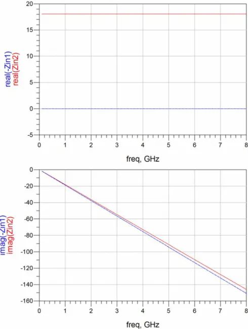
Similarly, the NIC loaded with 2.9-nH inductor is simulated, and the simulated impedance shows between the sources of the two transistors is shown in Figure 3.16 with the impedance of an ideal −2.9-nH inductor for comparison. In addition, the impedance of the loads (the 1-pF capacitor and the 2.9-nH inductor) used in the NICs and their ideal counterparts (with minor adjustments to the value of the ideal
components) are shown in Figure 3.17 and Figure 3.18. The inversion of load reactance is still valid up to 3GHz, which can be observed between the sources of the two
transistors. Although there is a small input resistance that may be undesirable, it could be eliminated with slight change of the load based on Equation 2.6. From the similar behavior of the proposed circuit and an ideal NIC, it can be seen that the components’
parasitic effects would only slightly affect the NIC’s behavior at UHF if the components are properly chosen.
40
Figure 3.11 Input impedance of the 1-μF capacitor (circle line: reactance)
Figure 3.12 Impedance of the 560-nH inductor (circle line: reactance)
Figure 3.13 Impedance of the 120-nH inductor (circle line: reactance)
41 Figure 3.14 NIC consists of practical circuit components
Figure 3.15 Impedance of NIC loaded with 1-pF capacitor compared with ideal −1.2 pF capacitor
(circle line: ideal −1.2 pF capacitor)
42
Figure 3.16 Impedance of NIC loaded with 2.9-nH inductor compared with ideal −2.9 nH inductor
(circle line: ideal −2.9 nH inductor)
Figure 3.17 Impedance of the 1-pF load and an ideal 1-pF capacitor (circle line: ideal 1-pF capacitor)
Figure 3.18 Impedance of the 2.9-nH load and an ideal 2.6-nH inductor (circle line: ideal 2.6-nH
inductor)
43
Chapter 4
Implementation of the NIC
A prototype NIC circuit is simulated and manufactured based on the results in chapter 3. Simulations in this chapter are the extensions of that in the previous chapter.
Apart from the components’ non-ideal behavior, the effects of transmission lines and the substrate are also included in the simulations presented in this chapter. The conclusion and future works are addressed at the end of this chapter.
4.1 Simulation of the prototype NIC circuit
The geometry of the prototype NIC circuit is shown in Figure 4.1. The NIC circuit which is based on microstrip structure is simulated using ADS, and the schematic design is shown in Figure 4.2. The core of the NIC is shown in Figure 4.3, which consists of the two transistors, the DC block capacitors and the load impedance. A 1.6 mm FR4 dielectric slab (εr = 4.4 and tanδ=0.02) is used in this design. The load of the NIC circuit is a 1pF capacitor from Murata GRM15 series.
The simulated S-parameters for the 2-port NIC circuit are shown in Figure 4.4. The circuit is designed as a 2-port network, thus it can be easily measured and tested. The
44
impedance between the sources of the two transistors can be obtained by de-embedding the network after the measurement process.
Figure 4.1 Geometry of the prototype NIC
Figure 4.2 Schematic design of the prototype NIC used in the simulation
45 Figure 4.3 Core of the prototype NIC
Figure 4.4 Simulated S-parameters of the 2-port NIC network
46
The schematic design for simulating the impedance between the sources of the two transistors is shown in Figure 4.5, and the simulation result is shown in Figure 4.6. The simulation result in the previous chapter, which excludes the effects of the transmission line and the substrate, is also shown in Figure 4.6.
Figure 4.5 Schematic design for simulating the impedance between the sources of the two transistors
Figure 4.6 Simulated impedance between the sources of the two transistors (circle line: without the
effects of the transmission lines and the substrate)
47
4.2 Fabrication of the prototype NIC circuit
A photograph of the fabricated loaded NIC is shown in Figure 4.7. The size of this prototype circuit is 24×17 mm2, including the space occupied by the pads for SMA connectors and the DC connectors. If the area occupied by the biasing circuit and the connectors’ pads is neglected, the core of the NIC is implemented in the area equal to 2×2.8 mm2. At the submission date of this thesis, the measurement of the prototype NIC circuit is unfinished, thus the measurement results are not shown here.
Figure 4.7 Photograph of the prototype NIC
4.3 Conclusion
The frequency response of a NIC structure which is originally designed for LF (low frequency) is discussed in this thesis. By analyzing the new circuit model proposed in this thesis, the behavior of the NIC structure can be explained at UHF (ultra-high
48
frequency). The frequency response caused by the transistor is discussed in chapter 2, and the frequency response caused by the non-ideal surface-mounted devices used in the design is discussed in chapter 3.
A prototype UHF NIC is designed, simulated and fabricated. The general
components selection guide for a wideband UHF NIC is proposed in chapter 3, and the full prototype NIC circuit is discussed in this chapter. Although the frequency response of the NIC structure could be complicated at UHF, the simulations show that by
choosing the components properly and minimizing the size of the NIC structure, a wideband NIC at UHF is still possible to achieve.
4.4 Future works
There are some possible studies that could be the extension of this work, and they are divided into three categories. First, after the measurement of the NIC circuit is finished, the layout of the NIC could be further optimized based on the measurement results. Second, the small signal NIC circuit model proposed in this work could be modified into a more general form. By substituting general impedances for the internal capacitances of the transistor in the model, the frequency response of the full NIC circuit could be fully described, which includes the parasitic effects introduced by other
49
components in the circuit. Third, the circuit could be redesigned based on different applications. For instance, if a certain impedance-frequency curve is desired within a target frequency band (rather than the whole UHF band), the circuit could be redesigned based on the design formulas in chapter 2, and the optimal components choices could be different from that suggested in chapter 3. In addition, it should be noticed that the cross-couple pair (XCP) circuit used in the design is not necessarily operated as a NIC if components with more parasitic effects are adopted. Although not recommended for a NIC, these components could be adopted in the XCP circuit to synthesize the needed impedance by carefully making use of their parasitic effects. For example, wider transistors could be a better choice than the smaller ones if a large-value negative resistor is desired at the terminals of the XCP. However, the load of the XCP should be carefully selected, and it would not be simply the inverse of the desired negative resistor.
50
Reference
[1] S. E. Sussman-Fort and R. M. Rudish, "Non-Foster impedance matching of electrically-small antennas," Antennas and Propagation, IEEE Transactions on, vol. 57, pp. 2230-2241, 2009.
[2] B. Razavi, "The Cross-Coupled Pair - Part I [A Circuit for All Seasons]," Solid-State Circuits Magazine, IEEE, vol. 6, pp. 7-10, 2014.
[3] J. G. Linvill, "Transistor Negative-Impedance Converters,"
Proceedings of the IRE, vol. 41, pp. 725-729, 1953.
[4] H. Morkner, "Wafer scale package construction and usage for RF through millimeter wave applications," in Microwave Conference, 2009. EuMC 2009. European, 2009, pp. 1772-1775.
[5] O. O. Tade, P. Gardner, and P. S. Hall, "Antenna bandwidth broadening with a negative impedance converter," International Journal of Microwave and Wireless Technologies, vol. 5, pp. 249-260, 2013.
[6] Murata. SimSurfing [Online]. Available:
http://ds.murata.co.jp/software/simsurfing/en-us/index.html