Schottky barrier height and interfacial state density
on oxide-GaAs interface
J. S. Hwang,a)C. C. Chang, M. F. Chen, C. C. Chen, K. I. Lin, and F. C. Tang Department of Physics, National Cheng Kung University, Tainan, Taiwan
M. Hong and J. Kwo
Bell Laboratories, Lucent Technologies, Murray Hill, New Jersey 07974 共Received 15 November 2002; accepted 9 April 2003兲
Photoreflectance 共PR兲 and Raman spectra were employed to investigate the interfacial characteristics of a series of oxide films on GaAs. The barrier heights across the interfaces and the densities of interfacial states are determined from the PR intensity as a function of the pump power density. The oxide-GaAs structures fabricated by in situ molecular beam epitaxy exhibit low interfacial state densities in the low 1011 cm⫺2 range. The density of the interface states of the Ga2O3(Gd2O3) – GaAs structure is as low as (1.24⫾0.14)⫻1010cm⫺2. The Ga2O3(Gd2O3) dielectric film has effectively passivated the GaAs surface. Additionally, Raman spectra were used to characterize the structural properties of the oxide films. © 2003 American Institute of Physics. 关DOI: 10.1063/1.1578528兴
I. INTRODUCTION
Dielectric or insulating films have played an important role in fabricating conventional and low dimensional field-effect metal–insulator conductor devices.1–5 However, for high mobility materials such as GaAs and its related com-pounds, which are the most commonly used in low power, high-speed devices, an insulating film with low interface state density and stable device operation is not yet available. A large density of surface or interfacial states tends to pin the Fermi level in the energy gap and results in lower gain and speed of bipolar transistors, high loss in semiconductor la-sers, and low efficiency in solar cells and photodetectors. Several efforts have been made to search for dielectric films such as Si3N4, SiO2, Al2O3 and Ga2O3, deposited in com-bination with dry, wet and photochemical surface treatment.6 –9Recently, M. Passlack and co-workers10–12 of Bell Laboratory have reported an approach to growing, by in situ molecular beam epitaxy, a Ga2O3(Gd2O3) – GaAs struc-ture with interface state density in the low 1010 cm⫺2eV⫺1 range and interface recombination velocity of 4500 cm/s. They made capacitance–voltage (C – V), capacitance-time (C – T), conductance–voltage (G – V) and steady state photoluminescence 共PL兲 measurements to elucidate elec-tronic interface properties.13 More recently, the Bell Labs group has demonstrated enhancement-mode metal–oxide– semiconductor field-effect transistors 共MOSFETs兲 with in-version, using Ga2O3(Gd2O3) as the gate dielectric and a conventional ion implantation process.14 –16
Because of its contactless and nondestructive nature, modulation spectroscopy of photoreflectance 共PR兲 has be-come important in studying the surface barrier height,17–19 surface Fermi level pinning,20,21 surface state density,22–25
and doping concentration23 during the last three decades. Previous work has demonstrated that soft x-ray photoemis-sion spectroscopy共SXPS兲,26 –30used in most previous studies of the surface Fermi level, can be replaced by photoreflec-tance when investigating surface and interface Schottky bar-rier formations as well as surface Fermi level pinning. In our previous report, we presented results of our studies on the electronic properties of the oxide–semiconductor interface by photoreflectance. Four samples, air-, Al2O3– , Ga2O3– , and Ga2O3(Gd2O3) – GaAs 共bare GaAs surface兲 were stud-ied. From the observed Franz–Keldysh oscillations 共FKOs兲 of the PR spectra we were able to estimate the interface electric fields and the densities of interfacial states for air-, Al2O3– , and Ga2O3– GaAs interfaces. The density of inter-facial states of Ga2O3(Gd2O3) – GaAs was estimated from the low field limit criterion in photoreflectance spectroscopy, since no FKOs appear in PR spectra within the low field limit.
This study determines the barrier heights across the in-terfaces and the densities of interfacial states of air-, Al2O3– , Ga2O3– , and Ga2O3(Gd2O3) – GaAs from the PR intensity as a function of the pump power density. Moreover, Raman spectroscopy was also used to characterize the struc-tural characteristics of the epitaxial films. A coherent picture can be drawn from results obtained from previous and present PR studies, Raman spectroscopy and other studies. II. THEORY
In PR, the electric field of the sample is modulated through changes in the surface photovoltage induced by the absorption of photons with energy above the band gap en-ergy. When an electric field is applied to a sample, the elec-trons and holes are accelerated by the field. The line shape of the PR signal, ⌬R/R, is directly related to the perturbed dielectric function. In the low field limit,兩ប⍀兩3/⌫3⬍1/3, the line shape of the PR spectrum can be fitted to9,10
a兲Author to whom correspondence should be addressed; electronic mail: [email protected]
348
⌬R/R⫽RebAei共E⫺E
g⫹i⌫兲⫺ᐉc, 共1兲
where A is the amplitude, the phase angle, E the incident photon energy, Eg the interband transition energy, ⌫ the broadening parameter,ᐉ a parameter depending on the type of critical point (ᐉ⫽5/2 for a three-dimensional critical point兲, and ប⍀ is electro-optical energy defined by8
共ប⍀兲3⫽共បFe兲2/2, 共2兲
where F is the electric field and is the reduced interband electron and heavy hole pair effective mass in the direction of the electric field. For a moderate electric field, the PR spectrum exhibits a series of oscillations 共FKOs兲. The asymptotic expression for the FKO line shape is given by31–33 ⌬R/R⬃E⫺2共E⫺E g兲⫺1exp
冉
⫺ ⌫共E⫺Eg兲1/2 共ប⍀兲3/2冊
⫻cos冋
2 3冉
E⫺Eg ប⍀冊
3/2 ⫹册
, 共3兲where is an arbitrary factor. The extremes of the FKO in Eq. 共3兲 occur when
n⫽共4/3兲关共En⫺Eg兲/ប⍀兴3/2⫹, n⫽1, 2, 3, . . . , 共4兲 where n represents the index number of the FKO extremes. A plot of (4/3)(En⫺Eg)3/2 versus the index number n will
yield a straight line with slope (ប⍀)⫺3/2. Therefore, the electric field F can be obtained directly from the period of the FKOs.
The mechanism of the built-in electric field can be inter-preted by a simple model of the parallel plate capacitor. The band bending region which supplies the PR signal is sand-wiched between the negative charges in the interface states 共surface states for an air-GaAs structure兲 and the positive charges in the thin depletion layer in n-type GaAs. The elec-tric field of the capacitor is given by
F⫽i/0⫽eDi/0, 共5兲
wherei,, 0, e and Direpresent the charge density,
rela-tive dielectric constant, free space permittivity, free electron charge and density of the occupied interfacial states, respec-tively. Once the electric field is obtained from the FKOs, the interfacial charge density i and thus the interfacial state
density Di can be calculated from Eq.共5兲. For samples with
built-in electric field within the low field limit, their PR spec-tra do not exhibit Franz–Keldysh oscillations. The built-in electric fields can only be estimated from the low field limit criterion, 兩ប⍀兩3/⌫3⬍1/3. The only information provided by the PR spectra is that the built-in electric field and surface or interfacial state densities are smaller than those calculated from兩ប⍀兩3/⌫3⫽1/3.
An alternative approach can be taken to derive precisely the surface or interfacial state densities independent of whether the built-in electric fields are below the low field limit or in the moderate field regions. Under low-intensity low-frequency modulation, the PR intensity ⌬R/R, at fixed probe wavelength, is directly proportional to the modulating photovoltage (Vs) induced by the pump beam, and is given
by34 –38
⌬R/R⬀Vs⫽
kT
e ln共Ipc/I0⫹1兲, 共6兲
where is an ideality factor;39 Ipcis equal to the photocur-rent density Jpc times the surface area Apc simultaneously illuminated by both the pump and probe beams, and I0 ⫽I0(T) represents the saturation current, which depends on the dominant current flow mechanism40 and is equal to the saturation flow density J0(T) times an effective area A0, which effectively contributes to the current mechanism. The photocurrent density Jpcincludes the drift and diffusion cur-rent densities. According to curcur-rent–transport theory applied to the case in which the diffusion length is much larger than the penetration depth of the pump beam, Jpc can be written as37,38,41
Jpc⫽ePm␥共1⫺R0兲/ប, 共7兲
where Pmis the pump beam power density,␥is the quantum
efficiency, R0 is the reflectivity of sample surface andបis the photon energy of the pump beam.
Thermionic emission and diffusion are the main contri-butions to J0(T) so J0 can be expressed as
14,25,38,40
J0共T兲⫽bA*T2/共1⫹BT3/2兲cexp关⫺eVb共T兲/kT兴, 共8兲
where A* is the modified Richardson constant defined as m*ek2/(22ប3); V
bis the barrier height across the interface
or the surface barrier height on the bare surface, and B ⫽(k/2m*)1/2(300/0),42where m*is the effective mass of the electron. Substituting Eqs. 共7兲 and 共8兲 into Eq. 共6兲 with Ipc⫽ApcJpcand I0⫽A0J0 yields a PR intensity of
⌬R/R⫽共kT/e兲lnb1⫹ePm␥共1⫺R0兲共1⫹BT3/2兲
⫻exp共eVb/kT兲/បrA*T2c, 共9兲
where r⬅A0/Apc is defined as the geometric factor intro-duced by Yin et al.26
At constant temperature, the only variable in Eq. 共9兲 is the pump beam power density Pm. When experimental
val-ues⌬R/R at various pump beam intensities are least squares fitted to Eq.共9兲, Vb,and r can be obtained from the fitting
parameters. The density of surface or interfacial states is then calculated from rN0 where N0 is the number of atoms per unit area of the surface.
III. EXPERIMENT
The samples were grown using an ultrahigh vacuum 共UHV兲 multiple-chamber molecular beam epitaxy 共MBE兲 system. A typical growth sequence entailed different oxide films being deposited on a 1.5 m n-type GaAs buffer layer (1.6⫻1016cm⫺3) which had previously been grown on a highly doped n-type共100兲 GaAs substrate. The oxide films, Al2O3– , Ga2O3– , and Ga2O3(Gd2O3) – GaAs, were depos-ited using molecular beams of aluminum oxides, gallium ox-ides, and a mixture of gallium oxides and gadolium oxox-ides, respectively. Single crystals of Al2O3, Ga2O3, and Gd3Ga5O12were used as source materials and evaporated by the e-beam technique. According to the work reported by Passlack et al.,10the use of Gd3Ga5O12was motivated by the unavailability of single Ga2O3crystal and led to the
success-ful deposition of gallium oxide molecules that formed ex-tremely uniform nonstoichiometric Ga2O3(Gd2O3) films on GaAs. Samples with different dielectric film materials and thickness are listed in Table I.
A standard PR apparatus was used in this study. The probe beam consisted of a tungsten lamp and a 1/4 m mono-chromator. A He–Ne laser served as the pump beam. The detection scheme consisted of a Si photodetector and a lock-in amplifier. The probe and pump beams were defo-cused onto the sample to reduce the photovoltaic effect. All measurements were performed at room temperature and modulation frequency of 200 Hz. The dependence of the PR intensity on the pump beam intensity was measured with the wavelength of the probe beam fixed at one of the two major extremes of the PR spectrum. The pump beam intensity, con-trolled by a gradient neutral density filter, was varied from 0.3 to 1000W/cm2. Data were measured by a computerized acquisition system.
Raman scattering experiments were performed in back-scattering geometry on sample surfaces using an Ar⫹-ion laser. Raman spectra of III–V compound semiconductors with zinc-blende crystal structure generally show two peaks. The lower-frequency peak corresponds to transverse optical 共TO兲 phonons while the higher peak corresponds to longitu-dinal optical 共LO兲 phonons. Only LO phonons appear in the 共100兲 backscattering direction, and only TO phonons appear in the 共110兲 direction, while both appear in the 共111兲 direction.43,44The laser output power was fixed at 100 mW so as to prevent excess heating of the samples and was fo-cused onto the samples by a cylindrical lens. The light scat-tered was analyzed using a standard double-grating spec-trometer in photon-counting mode, and the spectral resolution was better than 2 cm⫺1.
IV. RESULTS AND DISCUSSION
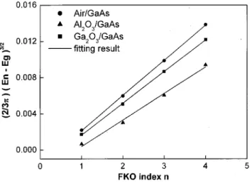
Figure 1 displays the PR spectra for all samples at room temperature measured at a pump beam power of 1W/cm2. The spectra of air-, Al2O3– , and Ga2O3– GaAs samples ex-hibit FKO features 共labeled A–D in Fig. 1兲 with different periods above the energy gap of GaAs共1.42 eV兲. They indi-cate that electric fields of various strengths exist in the inter-face regions of the samples and that the strengths of these fields are above the low field limit. In Fig. 2, (4/3)(En ⫺Eg)3/2is plotted as a function of the extreme index n in the
spectra. The solid lines are linear fits to Eq.共4兲. The slope of the solid line yields the electro-optic energy ប⍀, which in
turn gives the built-in electric field F. The effective masses of the electrons and heavy holes in GaAs used here are 0.065 and 0.34m0, respectively, where m0 is the free electron mass. Once the electric field is determined from the FKOs, the interfacial charge density i, and thus the occupied interfacial state density Di can be calculated from Eq. 共5兲.
No FKO feature appears in the spectrum of
Ga2O3(Gd2O3) – GaAs, implying that the electric field in this sample is too low to create any FKOs and that the only feature seen in the spectrum corresponds to the fundamental band to band transition. The broadening parameter ⌫, ob-tained by fitting the corresponding PR spectrum to Eq.共1兲, is 13 meV, measured at a pump beam power density of 1
W/cm2. Electric field F corresponds to the low field crite-rion, 兩ប⍀兩3/⌫3⬍1/3, which at this broadening parameter is less than 2.1⫻104 V/cm. Accordingly, the interfacial state density of Ga2O3(Gd2O3)-GaAs estimated from Eq. 共5兲 is less than 1.0⫻1011cm⫺2. Table I lists the results for all samples.
FIG. 1. PR spectra of samples of air-, Al2O3– , Ga2O3– , and
Ga2O3(Gd2O3) – GaAs at room temperature.
FIG. 2. Quantity (4/3)(En⫺Eg)3/2, as a function of index n of the FKO
extrema. TABLE I. Sample structure, oxide film thickness, values of the interfacial
field, and densities of interfacial states Diestimated from the model of the
parallel capacitor. Dielectric film Thickness 共Å兲 F 共kV/cm兲 (1011cmD⫺2i eV⫺2) Air 48 2.4 Al2O3 700 44 2.2 Ga2O3 600 38 1.9 Ga2O3(Gd2O3) 400 ⬍21a ⬍1.0
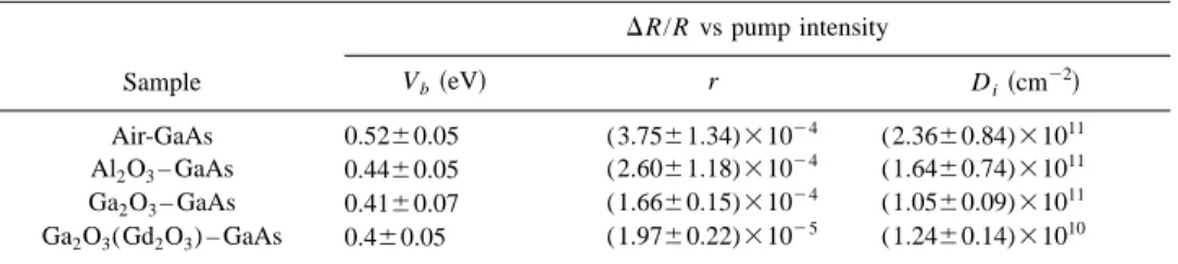
Figure 3 presents the PR spectra of all samples at room temperature measured at various pump power densities. Fig-ure 4 depicts the PR intensity (⌬R/R) as a function of pump power density for all samples. For each sample, the PR sig-nal was measured with the probe beam wavelength fixed at the major extreme prior to the band gap energy in the PR spectra. The solid lines are the least-squares fits obtained using Eq.共9兲. For GaAs samples, when A*⫽8.0 A/cm2K2, B⫽3.3⫻10⫺4K⫺3/2, ␥⬵1, N0⫽6.3⫻1014cm⫺2, and R0 ⫽0.34, the fitting parameters are Vb, , and r. Table II lists
the fitting parameters obtained and the densities of interfacial states Di calculated from rN0. The densities of interfacial states determined by both approaches are comparable and are in the low 1011cm⫺2 range for air-, Al2O3– , and Ga2O3– GaAs. For Ga2O3(Gd2O3) – GaAs, Di is as low as
(1.24⫾0.14)⫻1010cm⫺2, implying that the GaAs surface is effectively passivated by the Ga2O3(Gd2O3) dielectric film.45,46The results are also consistent with those reported by Passlack et al.10–12who determined Difrom capacitance–
voltage measurements in quasistatic/high frequency modes. Hong and co-workers46,47 attributed the low Di in
Ga2O3(Gd2O3) – GaAs to the formation of bonding between Gd2O3 and GaAs.
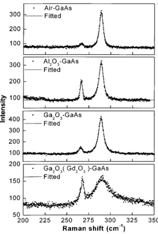
Figure 5 shows Raman spectra of all samples. Each spectrum shows a strong peak at 290⫾2 cm⫺1 and a weak peak at 266⫾2 cm⫺1 that represent the LO and TO modes, respectively. As stated earlier, only the LO mode is allowed in共100兲 oriented material. However, a peak associated with the TO mode is also observed, probably because of a slight substrate misorientation or imperfection or perhaps a small experimental deviation from backscattering. This phenom-enon was also observed with other 共100兲 oriented III–V semiconductors.
Each peak in the Raman spectra of all of the samples was fitted to a Lorentzian line shape to determine its ampli-tude, position, and full width at half maximum 共FWHM兲. The solid lines in Fig. 5 represent the theoretical fits. Table III lists the results for LO modes. The results for TO modes are not considered here since they follow from substrate mis-orientation or imperfection of the substrate, or a small ex-perimental deviation from backscattering. Notably, Ga2O3(Gd2O3) – GaAs, which has the lowest interface state density, has the lowest Raman peak intensity and the greatest FIG. 3. PR spectra of all samples at room temperature measured under
various pump beam power densities.
FIG. 4. PR intensity as a function of the pump beam power density.
TABLE II. Interfacial barrier height, geometric factor, and densities of interfacial states Diderived from the PR
intensity as functions of the pump power density.
Sample ⌬R/R vs pump intensity Vb共eV兲 r Di共cm⫺2兲 Air-GaAs 0.52⫾0.05 (3.75⫾1.34)⫻10⫺4 (2.36⫾0.84)⫻1011 Al2O3– GaAs 0.44⫾0.05 (2.60⫾1.18)⫻10⫺4 (1.64⫾0.74)⫻1011 Ga2O3– GaAs 0.41⫾0.07 (1.66⫾0.15)⫻10⫺4 (1.05⫾0.09)⫻10 11 Ga2O3(Gd2O3) – GaAs 0.4⫾0.05 (1.97⫾0.22)⫻10⫺5 (1.24⫾0.14)⫻1010
FWHM, because Ga2O3(Gd2O3) film on GaAs is a nano-crystalline film that consists of small grains of either Ga2O3 or Gd2O3, whereas Al2O3 and Ga2O3 films are amorphous and polycrystalline, respectively, with each a single oxide with preferred orientation. A nanocrystalline film of two dif-ferent oxide grains usually has a less intense wider Raman peak. In addition, Hong et al.47,48 found, using reflection high energy electron diffraction共RHEED兲 and x-ray diffrac-tion, that the first few molecular layers of Ga2O3(Gd2O3) oxides grown on GaAs include only Gd2O3 single crystals while the layers grown subsequently include a mixture of Ga2O3 and Gd2O3 oxides. Their conclusions are consistent with the features of the Raman spectra obtained herein, since the existence of Gd2O3 single crystal epitaxial film further reduces the intensity and increases the width of the Raman peak.
V. CONCLUSIONS
The contactless nondestructive technique of photoreflec-tance was employed to determine the barrier heights and densities of interfacial states of a series of oxide-GaAs struc-tures. In contrast to in the authors’ previous report, which estimated the interfacial state densities by assuming that the band bending region across the interface was a parallel ca-pacitor, this study accurately determines the interfacial state density from the PR intensity as a function of the pump power density. The densities of interfacial states obtained match the results of our previous report and also those obtained from capacitance–voltage measurements in quasistatic/high frequency modes. The oxide-GaAs struc-tures fabricated by in situ molecular beam epitaxy were found to exhibit low interfacial state densities, in the low 1011 cm⫺2 range. The density of interface states of Ga2O3(Gd2O3) – GaAs is as low as (1.24⫾0.14) ⫻1010 cm⫺2. The Ga
2O3(Gd2O3) dielectric film has effec-tively passivated the GaAs surface. Moreover, Raman spec-tra were used to characterize the structural properties of the oxide films.
ACKNOWLEDGMENT
This work was supported by National Science Council of the Republic of China under Contract No. NSC 90-2112-M-006-029.
1W. E. Spicer et al., J. Vac. Sci. Technol. B 6, 1245共1988兲.
2L. S. Hung, G. H. Braunstein, and L. A. Bosworth, Appl. Phys. Lett. 60, 201共1992兲.
3
P. Viktorovitch, M. Gendry, S. K. Krawczyk, F. Krafft, P. Abraham, A. Bekkaoui, and Y. Monteil, Appl. Phys. Lett. 58, 2387共1991兲.
4H. Shigekawa, T. Hashizume, H. Oigawa, K. Motai, Y. Mera, Y. Nannichi, and T. Sakurai, Appl. Phys. Lett. 59, 2986共1991兲.
5J. A. Dagata, W. Tseng, J. Bennett, J. Schneir, and H. H. Harary, Appl. Phys. Lett. 59, 3288共1991兲.
6F. Capasso and G. F. Williams, J. Electrochem. Soc. 129, 821共1982兲. 7S. D. Offsey, J. M. Woodall, A. C. Warren, P. D. Kirchner, T. I. Chappell,
and G. D. Pettit, Appl. Phys. Lett. 48, 475共1986兲. 8
C. J. Sandroff, R. N. Nottenburg, J.-C. Bischoff, and R. Bhat, Appl. Phys. Lett. 51, 33共1987兲.
9J. S. Herman and F. L. Terry, Appl. Phys. Lett. 60, 716共1992兲. 10M. Passlack, M. Hong, J. P. Mannaerts, S. N. G. Chu, R. L. Opila, and N.
Moriya, Tech. Dig. - Int. Electron Devices Meet. 1995, 383. 11
M. Hong, M. Passlack, J. P. Mannaerts, J. Kwo, S. N. G. Chu, N. Moriya, S. Y. Hou, and V. J. Fratello, J. Vac. Sci. Technol. B 14, 2297共1996兲. 12M. Passlack, M. Hong, J. P. Mannaerts, R. L. Opila, S. N. G. Chu, N.
Moriya, F. Ren, and J. R. Kwo, IEEE Trans. Electron Devices 44, 214
共1997兲. 13
M. Passlack et al., J. Appl. Phys. 77, 686共1995兲.
14M. Hong, J. Kwo, A. R. Kortan, J. P. Mannaerts, and M. Sergent, Science 共Washington, DC, U.S.兲 283, 1897 共1999兲.
15F. Ren, J. M. Kuo, M. Hong, W. S. Hobson, J. R. Lothian, and J. Lin, IEEE Electron Device Lett. 19, 309共1998兲.
16M. Hong, F. Ren, J. M. Kuo, W. S. Hobson, J. P. Mannaerts, J. R. Lothian, and Y. K. Chen, J. Vac. Sci. Technol. B 16, 1398共1998兲.
17X. Yin, H. M. Chen, F. H. Pollak, Y. Chan, P. A. Montano, P. D. Kirchner, G. D. Pettit, and J. M. Woodall, Appl. Phys. Lett. 58, 260共1991兲. 18
J. S. Hwang, Z. Hang, S. L. Tyan, S. W. Ding, J. H. Tung, C. Y. Cheng, B. J. Lee, and J. T. Hsu, Jpn. J. Appl. Phys., Part 2 31, L571共1992兲. 19J. S. Hwang and S. L. Tyan, J. Vac. Sci. Technol. A 10, 3176共1992兲. 20H. Shen, M. Dutta, L. Fotiadis, P. G. Newman, R. P. Moerkirk, W. H.
Chang, and R. N. Sacks, Appl. Phys. Lett. 57, 2118共1990兲. 21
C. Van Hoof, K. Deneffe, J. De Boeck, D. J. Arent, and G. Borghs, Appl. Phys. Lett. 54, 608共1989兲.
FIG. 5. Raman spectra of all samples at room temperature.
TABLE III. Amplitude, center position, and FWHM of the LO mode of the Raman spectra at room temperature.
Sample
Vibration mode:LO
Amplitude Center共cm⫺1兲 Half width 共cm⫺1兲
Air-GaAs 259.1 289.1 4.7
Al2O3– GaAs 236.0 289.1 5.7
Ga2O3– GaAs 324.8 289.2 6.7
22J. S. Hwang, W. Y. Chou, S. L. Tyan, H. H. Lin, and T. L. Lee, Appl. Phys. Lett. 67, 2350共1995兲.
23R. N. Bhattacharya, H. Shen, P. Parayanthal, F. H. Pollak, T. Coutts, and H. Aharoni, Phys. Rev. B 37, 4044共1988兲.
24X. Yin, F. Pollak, L. Pawlowicz, T. O’Neill, and M. Hafazi, Appl. Phys. Lett. 56, 1278共1990兲.
25
See, for example, J. M. Woodall, P. D. Kirchner, J. L. Freeouf, and A. C. Warren, Solid-State Electron. 33, 53共1990兲, and references therein. 26X. Yin, H.-M. Chen, F. H. Pollak, Y. Chen, P. H. Montano, P. D. Kirchner,
G. D. Pettit, and J. M. Woodall, J. Vac. Sci. Technol. A 10, 131共1992兲. 27
S. Chang, L. J. Brillson, Y. J. Kime, D. S. Rioux, P. D. Kichner, G. D. Pettit, and J. M. Woodall, Phys. Rev. Lett. 64, 2551共1990兲.
28T. T. Chiang, C. J. Spindt, W. E. Spicer, I. Lindau, and R. Browning, J. Vac. Sci. Technol. B 16, 1409共1998兲.
29M. Yamsda, A. K. Wahi, P. L. Meissner, A. Herrera-Gomez, T. Ken-delewicz, and W. E. Spicer, Appl. Phys. Lett. 58, 2243共1991兲. 30T. T. Chiang and W. E. Spicer, J. Vac. Sci. Technol. A 7, 724共1989兲. 31J. S. Hwang, Y. C. Wang, W. Y. Chou, S. L. Tyan, M. Hong, J. P.
Man-naerts, and J. Kwo, J. Appl. Phys. 83, 2857共1998兲. 32
N. Bottka, D. K. Gaskill, R. J. M. Griffiths, R. R. Bradley, T. B. Joyce, C. Ito, and D. McIntyre, J. Cryst. Growth 93, 481共1988兲.
33T. M. Hsu, Y. C. Tien, N. H. Lu, S. P. Tsai, D. G. Liu, and C. P. Lee, J. Appl. Phys. 72, 1065共1992兲.
34H. Hovel, Semiconductors and Semimetals共Academic, New York, 1975兲, Vol. 11, p. 59.
35X. Yin, H.-M. Chen, F. H. Pollak, Y. Chan, P. A. MonTano, P. D. Kirchner, G. D. Pettit, and J. M. Woodall, J. Vac. Sci. Technol. A 10, 131共1992兲.
36H. Shen and M. Dutta, J. Appl. Phys. 78, 2151共1995兲, and references therein.
37G. S. Chang, W. C. Hwang, Y. C. Wang, Z. P. Yang, and J. S. Hwang, J. Appl. Phys. 86, 1765共1999兲.
38
J. S. Hwang, G. S. Chang, W. C. Hwang, and W. J. Chen, J. Appl. Phys.
89, 1771共2001兲.
39S. M. Sze, Semiconductor Devices Physics and Technology共Wiley, New York, 1985兲.
40M. Hecht, Phys. Rev. B 41, 7918共1990兲. 41
T. Kanata, M. Matsunaga, H. Takakura, Y. Hamakawa, and T. Nishino, Proc. SPIE 1286, 56共1990兲.
42H. Shen, S. H. Pan, Z. Hang, J. Leng, F. H. Pollak, J. M. Woodall, and R. N. Sacks, Appl. Phys. Lett. 53, 1080共1988兲.
43C. S. Rama Rao, S. Sundaram, R. L. Schmidt, and J. Comas, J. Appl. Phys. 54, 1808共1983兲.
44
F. H. Pollak, Microelectronics-Applications, Materials and Technology
共SRI International, Menlo Park, CA, 1984兲, pp. 185–284.
45J. Kwo, D. W. Murphy, M. Hong, R. L. Opila, J. P. Mannaerts, A. M. Sergent, and R. L. Masaitis, Appl. Phys. Lett. 75, 1116共1999兲. 46J. Kwo, D. W. Murphy, M. Hong, J. P. Ma, R. L. Opila, and R. L. Masaitis,
J. Vac. Sci. Technol. B 17, 1294共1999兲.
47M. Hong, A. R. Kortan, J. Kwa, J. P. Manaerts, J. J. Krajewski, Z. H. Lu, K. C. Hsieh, and K. Y. Cheng, J. Vac. Sci. Technol. B 18, 1688共2000兲. 48
M. Hong, Z. H. Lu, J. Kwo, A. R. Kortan, J. P. Manaerts, J. J. Krajewski, K. C. Hsieh, L. J. Chou, and K. Y. Cheng, Appl. Phys. Lett. 76, 312