A Novel Single-Switch High Conversion Ratio DC---DC Converter Ching-Shan Leu and Shun-Yuan Wu
Power Conversion Laboratory Department of Electrical Engineering
National Taiwan University of Science and Technology Taipei, Taiwan, R.O.C 106
cleu@ mail.ntust.edu.tw
Abstract—By employing the coupled-inductor technique tothe two cascaded boost converters, a single-switch high conversion ratio DC---DC converter is proposed. Unlike its predecessor, high voltage gain can be obtained without operating at extreme duty cycle. In addition to the operating principles and the analysis, a 100 kHz 36-75V DC input, 400V/240W converter is implemented and tested. The 91.2%
maximum efficiency can be achieved under high-line 85% full load operation condition.
Index Terms—boost, DC-DC, high voltage gain ratio
I. I
NTRODUCTIONHigh step-up DC-DC converters are necessary in low input-voltage to high output-voltage power conversion applications. By employing the traditional boost converter with extreme duty cycle operation, the voltage gain approximates six times its applied voltage due to the losses of the parasitic components. However, at least ten times voltage gain is needed in many applications such as the front- end stage of the renewable energy systems, the DC bus of the telecom power systems and high intensity discharge (HID) lamp ballast for the automobile headlights. To obtain the required voltage gain, several topologies have been proposed by employing the coupled inductor or the cascaded booster converter techniques [1]-[12]. However, the former technique induces high voltage stress caused by the leakage inductance of the coupled inductor. On the contrary, the latter suffers from the synchronizing of the two power switches [9]. By merging both the coupled inductor and the cascaded techniques, a novel single-switch high conversion ratio DC---DC converter is thus proposed to alleviate these problems. In addition to the analysis and circuit principles, the circuit is implemented and tested to demonstrate its feasibility.
II. ANALYSIS AND CIRCUIT OPERATION
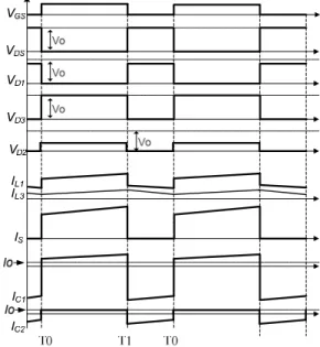
The circuit diagram and the key waveforms of the proposed converter are shown in Fig. 1 and Fig. 2, respectively. It consists a coupled-inductor with two windings, L1 and L2, with N ()N2:N1 turns-ratio, one switch S1, three diodes D1, D2, D3, one inductor L3, and two output capacitors, C1 and C2.
To simplify the analysis of the proposed converter, the capacitors, C1 and C2, are assumed to be sufficiently large that the voltages can be assumed to be constant. Figures 3(a) and 3(b) illustrate the equivalent circuits during the switch-on and the switch-off period, respectively. The
operation of the converter can be divided into two stages within one full switching cycle:
Fig. 1. Circuit diagram of the proposed converter.
Fig. 2 Key waveforms of the proposed converter.
[T0-T1]: When the switch S1 is turned on at T0, the diode D1 starts to conduct. Inductor L1 and L3 are charged by Vi and Vc1, respectively. In addition to charging the inductor L3, the voltage across the capacitor C1 provides power to the output load via the capacitor C2.
[T1-T0]: When the switch S1 is turned off at T1, the diode D1 is reverse-biased and the current of the IL1 and
PEDS2009
IL3 flows through the diode D2 and D3 to charge the capacitor C1 and C2, respectively. In addition to charging capacitors C1 and C2, the current I
L3provides the output load current Io and the current I
L1flows through the coupled inductor L1, L2 is decreased with a slope of (Vc1-Vi)/(L1+L2) to charge the capacitor C1.
Vi
L1
L2 L3
D1 D2
D3 C1
R C2 +Vo
Gnd Q
N1 N2
(a)
Vi
L1
L2 L3
D1 D2
D3 C1
R C2 +Vo
Gnd Q
N1 N2
(b)
Fig. 3 Equivalent circuit stages of the proposed converter.
From the voltage-second balance of the inductor L1, L3, the equations can be obtained as:
1
(1 ) 0
(1 )
C i
i
V V
V D D
N
⋅ + − − =
+ (1)
1
(
1)(1 ) 0
C C
V ⋅ + D Vo V − − D = (2)
The voltage gains of (V
C1/V
i) and (Vo/V
C1) can be derived as Eq. (3) and Eq. (4), respectively.
1
1
1
C i
V ND
V D
= +
− (3)
1
1 1
O C
V
V = D
− (4)
Therefore, the voltage gain of the proposed converter is derived as shown in Eq. (5).
2
1 (1 )
O i
V ND
V D
= +
− (5)
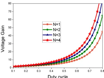
The ideal voltage gain verse the duty cycle is plotted with N as the running parameter as shown in Fig. 4. With a higher turns-ratio, N=4, the voltage gain be up to 20 by employing the proposed converter with 0.6 duty cycle.
Fig. 4 Ideal voltage gain verse duty cycle of the proposed converter
In practically, the inductor winding resistor, the forward voltage drop of the diode V
F, and MOSFET’s turn-on resistor r
DSare considered in deriving the voltage gain as follows:
Including the non-ideal components, the circuit diagram is shown in Fig .5.
Fig. 5 Circuit diagram of the proposed converter including inductor resistors (re1,re2 and re3), MOSFET’s turn-on resistor, rDS, and the diode forward voltage drop (VF1,VF2 and VF).
The Ampere-Second balance of the capacitors, C1 and C2, are expressed as Eq. (6) and Eq. (7), respectively.
3 2 3 2
( I
L+ Io D ) ⋅ − ( I − I
L+ I
C)(1 − D ) 0 = (6)
(
L3)(1 ) 0
Io D ⋅ − I − Io − D = (7)
Therefore, I
L3, I
2can be expressed as:
3
(1 )
L
I Io
= D
− (8)
PEDS2009
2
(1 )
2I Io
=
D− (9)
2 2 2
1 1 1 2
1 1
( 1)
2 L I = 2 L N + I (10)
Both terms in Eq. (10) represent the inductor energy under the switch S1 turned on-off transition.
As a result, I
1is expressed as
1 2 2
( 1) ( 1)
(1 ) N Io
I N I
D
= + = +
− (11)
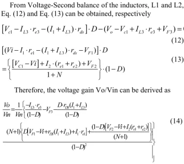
From Voltage-Second balance of the inductors, L1 and L2, Eq. (12) and Eq. (13) can be obtained, respectively
[ V
c1− I
L3⋅ − r
e3( I
1+ I
L3) ⋅ r
ds] ⋅ − D V V (
o−
c1+ I
L3⋅ + r
e3V
F3) 0 =
(12)
[ ]
[ ]
1 1 1 3 1
1 2 1 2 2
( ( ) )
( )
(1 ) 1
e L ds F
C e e F
Vi I r I I r V D V Vi I r r V
N D
− ⋅ − + ⋅ − ⋅
⎧ − + ⋅ + + ⎫
= ⎨ ⎬ ⋅ −
⎩ + ⎭
(13)
Therefore, the voltage gain Vo/Vin can be derived as
[ ] [ ]
3 3 1 3
3
2 2 1 2
1 1 3 1 1
2
( )
1
(1 ) (1 )
(1 ) ( )
( 1) ( )
( 1) (1 )
L e DS L
F
F e e
F DS L e
I r D r I I
Vo V
Vin Vin D D
D V Vi I r r N DV Vi r I I I r
N D
⎧− ⋅ ⋅ +
= ⎨ − −
− −
⎩
⎧ − − + + ⎫⎫
+ ⎨ − + + + ⋅ + ⎬⎪
+ ⎪
⎩ ⎭
− ⎬
− ⎪
⎪⎭
(14)
According to Eq. (14), the voltage gain verse duty cycle by using the turns-ratio of the coupled-inductor as the running parameter is plotted as shown in Fig. 6.
Fig. 6 Voltage gain verse duty cycle by using the turns ratio as the running parameter.
As illustrated, the maximum voltage gain is highly constrained by the ESRs of the inductors. However, to
obtain a higher voltage gain without operating at extreme duty cycle, higher turns-ratio of coupled inductor is recommended.
III. EXPERIMENT RESULTS
A 36-75 V input, 400 V output and 240 W output power converter is implemented. It operates at 100 KHz. The turns-ratio of the coupled-inductor, L2:L1, is set to 1:1.
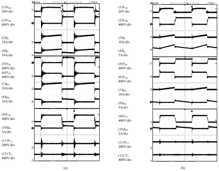
Figures 7(a) and 7(b) show the oscillograms of the key waveforms of the proposed converter under low-line full-load and high-line light-load operating conditions, respectively.
First, a high voltage gain (400/36=11) of the converter is verified as shown in channel 12 in each diagram. 400V output voltage is obtained with 0.62 duty cycle under low- line operating condition.
As shown in channel 2 in each diagram, the voltage waveform across the switch is spike free and clamped to 400V, Vo.
The voltage stress of the diodes can be read from channels 5, 6 and 9 of each diagram. As shown, D3 is clamped the output voltage, Vo. On the contrary, D1 and D2 are dependent on the operating conditions and are always smaller than the output voltage.
As shown in channel 11, the Vc1 is clamped to 160V and 200V for the low-line full load and high-line light load conditions, respectively.
Finally, the measured efficiency of the proposed converter under different line and load operating conditions is plotted in Fig. 8. As shown, the maximum efficiency 91.2% occurs at 75V input 400V/0.5A output operating condition
IV. CONCLUSIONS
By employing the coupled-inductor and cascaded- converter techniques, a single-switch high conversion ratio converter is proposed. A higher voltage gain is verified from the experimental results under low input voltage 36V operating condition. A 400V output-voltage is obtained with 0.62 duty cycle.
Moreover, the voltage waveforms of the switch S1 and diodes D1, D2, D3 are all well clamped without voltage spike.
A maximum 91.2% efficiency is achieved under high-line and 85% load operating condition. It can be further improved by paralleling the MOSFET and/or employing the MOSFET to replace the diodes.
Therefore, the proposed converter is favorable for the high conversion ratio power conversion applications.
PEDS2009
Fig. 7. Oscillograms of the converter under (a) low-line full-load, and (b) high-line light-load operating conditions.
Fig. 8. Measured efficiency of the power stage of the proposedconverter
REFERENCE
[1] K.C. Tseng, T.J. Liang. “Novel High Efficiency Step-up Converter”
IEE Proc. Electr. Power Applications, Vol 151, No 2, March 2004, pp.182-190.
[2] R.J. Wai, R.Y. Duan. “High Step-up Converter with Coupled-Inductor”
IEEE Transactions on Power Electronics, Vol 20, No 5, September 2005. pp 1025-1035.
[3]T.J. Liang, KC Tseng. “Analysis of Integrated Boost-Flyback Step-up Converter” IEE Proc. Electr. Power Applications, Vol 152, No 2, March 2005, pp.217-225.
[4] Q. Zhao, F.C. Lee. “High Efficiency, High Step-up DC-DC Converters”
IEEE Transactions on Power Electronics, Vol 18, No 1, January 2003.pp 65-73.
[5] Q Zhao, Fengfeng Tao, and Fred C. Lee, “A Front-End DC-DC Converter for Network Server Applications”, in Proc. IEEE-PESC’01, pp.1535-1539.
[6] R.J. Wai, C.Y. Lin, R.Y. Duan, and Y.R. Chang “High-Efficiency DC- DC Converter with High Voltage Gain and Reduced Switch Stress”
IEEE Transactions
[7]L. Huber and M. M. Jovanovic, “A design approach for server power supplies for networking,” in Proc. IEEE Appl. Power Electron. Conf., (1)VGS
20V/div
(2)VDS
400V/div
(3)IQ
10A/div
(4)Iin
10A/div
(5)VD1 400V/div (6)VD2
400V/div (7)ID1
10A/div
(8)ID2
10A/div
(9)VD3
400V/div
(10)ID3
5A/div
(11)VC1
200V/div
(12) Vo
400V/div
(a)
(1)VGS
20V/div
(2)VDS
400V/div
(3)IQ
10A/div
(4)Iin
5A/div
(5)VD1 400V/div
(6)VD2
400V/div
(7)ID1
10A/div
(8)ID2
5A/div
(9)VD3
400V/div
(10)ID3
2A/div
(11)VC1
200V/div
(12) Vo
400V/div
(b)
PEDS2009
2000, pp. 1163–1169. on Industrial Electronics, Vol. 54, No.1, February 2007. pp 354-364.
[8] N. Vazquez, L. Estrada, C. Hernandez, E. Rodriguez “The Tapped- Inductor Boost Converter” IEEE International Symposium on Industrial Electronics, June 2007 pp 538 – 543.
[9] F.L Luo, H. Ye. “Positive output cascade boost converters”. IEE Proc.
Electr. Power Applications, Vol 151, No 5, September 2005, pp.590- 606.
[10] Esam H. Ismail, Mustafa A. Al-Saffar, and Ahmad J. Sabzali, “High Conversion Ratio DC–DC Converters with Reduced Switch Stress”, IEEE TRANSACTIONS ON CIRCUITS AND SYSTEMS, VOL. 55, NO. 7, AUGUST 2008.
[11] Zhao, Q., Tao, F., Hu, Y., and Lee, F.C.: ‘Active-clamp DC/DC converters using magnetic switches’. Applied Power Electronics Conf.
(APEC 2001), Piscataway, NJ, USA, 2001, 2, pp. 946–952 [12] Copple, E.J., and Heights, A.: ‘High Efficiency DC Step-up Voltage
Converter’, US Patent’, 5929614, July 1999.