國立臺灣大學電機資訊學院電信工程學研究所 碩士論文
Graduate Institute of Communication Engineering College of Electrical Engineering and Computer Science
National Taiwan University Master Thesis
應用於第五代行動通訊之功率放大器與混頻器的研究 Research of Power Amplifier and Up-Conversion
Mixer for 5G Mobile Communications
王子豪 Ziu-Hao Wang
指導教授:王暉 博士 Advisor: Huei Wang, Ph.D.
中華民國 110 年 2 月 February, 2021
誌謝
本論文得以完成首先最感謝的是我的指導教授 王暉教授,在我碩士班生涯上 給予了專業上的建議以及時常提醒我需要保持積極的做事態度,老師平時的諄諄 教誨與細心指導引領學生進入毫米波的領域,讓我在研究所生涯從對電路懵懂無 知到最後得以從元件模型開始到最後設計電路與量測,老師兢兢業業的做事態度 讓我在英文上也有很大進步最後能順利完成投稿。同時,萬分感謝中研院天文所 的章朝盛博士,在量測以及在建模型上給予相當多的建議和幫助,碩士論文更是 仔細地批改並給予建議。此外,非常感謝口試委員們,黃天偉教授、林坤佑教授、
蔡作敏教授以及章朝盛博士提供許多珍貴的意見,使得碩士論文可以更加完整。
碩士生涯中在實驗室獲得許多幫助,感謝博士班學長陳俊年、王雲杉和吳依 靜學姊,尤其是年哥百忙之中抽空與我們小組討論進度,不管在學業上還是生活 上都對我非常關心。感謝碩士班學長姊陳穎、張洋、黃煒程、李凱皇、姜智尹、
唐子兼、呂柏澤、郭岱宥、許清閔、林彥廷和黎欣怡,從我還是菜鳥時候細心教 導給予許多意見,讓我能快速克服種種難關。另外感謝黃派學長們:鍾杰穎、林 文傑、林宜賢、黃幕召、吳茗航、江坤展、許皓翔、陳育群以及周佑運,在量測 以及研究上的指導,感謝文傑學長分享了很多量測上的知識,而且在我有問題的 時候都可以馬上回覆。同時感謝林派學長,高堃堯、黃致家、楊旻憲,感謝致家
學長當初不厭其煩的傾囊相授,讓我能順利完成Continuous Class-F-1的PA。感謝
碩班的同屆同學們,碧玲、庭瑄、毓閔、Pragya、彥廷、彥瑋、捷葦、昱廷、柏維、
宏博、聖凱,在我碩士班的生活中,大家互相學習奮鬥一起成長畢業,在生活上 也會互相關心增加我生活中許多樂趣,大家在畢業後仍會傳訊息彼此關心,令我 在碩士班最後一段日子感到暖心。特別感謝彥廷在我的工作以及愛情上給予幫 助,在我的人生之中意義重大。而在實驗室中的學弟妹牧恆、梓洋、煒智、楷儁、
威任、凱傑、友東、荷青、玟辰、宏源、雨鉉、瑋軒、愛晨、俊嘉、羚毓、傳立、
育成、健平、家頤,看到你們讓我想起當初在實驗室奮鬥的每一天,希望你們能 再繼續更努力下去,最後大家都能順利畢業。
最後我要感謝我的家人,對於我在學業上與人生道路上做的選擇都予以最大 的支持,讓我能全心全力在追求自己的目標。感謝我的女朋友,在我壓力最大的
那段日子裡給予我鼓勵與陪伴。我很幸運能遇到我的父母、好朋友們以及老師們,
沒有你們就沒有今天在這裡的我,期許未來的我能克服各種挑戰並回報給我珍愛 的人們。
中文摘要
本論文包含兩個部分都是希望運用在第五代行動通訊系統中。第一部分應用
在30 到 40 GHz 寬頻連續反 F 類功率放大器,使用 65 奈米金氧半場電晶體製程設
計。第二部分是應用於28 GHz 高線性度升頻器,使用 28 米金氧半場電晶體製程
設計。
論文中首先提出了一個應用在30 到 40 GHz 連續模式反 F(CCF-1)功率放大器
設計以同時達到寬頻且高效率的表現。此電路為了實現連續反 F 操作,利用輸出
變壓器並且在其中加入電容用來實現理想基頻與諧波阻抗設計。我們可以透過這 種方式設計來減少匹配電路的設計複雜度與損耗,除此之外,在本章當中也討論
放大器的線性度且電路的AM/PM 失真因為輸出諧波匹配而有一定程度的改善。量
測結果顯示本文提出的功率放大器在34 GHz 有 17.9 dBm 的飽和輸出功率且大訊
號頻寬包含從 30 到 40 GHz,在此輸出功率下仍有 35.8%功率附加效益,還得到
15 dBm 輸出功率的增益 1dB 壓縮點。在調變量測使用 64-QAM 的訊號下,此電路
達到 400MHz 調變頻寬且有 9.2 dBm 的平均輸出功率和 12.5 %平均功率附加效
率,且錯誤向量大小(EVM)小於-28 dB。
另外提出一個在轉導級使用二階交互調變注入技術達到高線性度的升頻器,
因此透過混和低頻輸入訊號和二階交互調變訊號可以在轉導級產生一個正的三階 交互調變訊號,並且透過電晶體操作在三級區來放大此訊號,最後本電路展現出 在寬輸入功率範圍下都有三階交互調變功率抑制。量測結果顯示此升頻器有-6.4 dB 的轉換增益與-2.2 dBm 輸出功率的增益 1dB 壓縮點,直流功率損耗為 19 mW,
而雙頻量測(two-tone measurement)則顯示明顯的三階交互調變功率抑制且輸出三
階截點功率為10.2 dBm。除此之外,在調變訊號量測使用 256-QAM 的訊號下,此
電路展現出在有三階交互調變失真抑制下輸出功率可以改善。
關鍵字:第五代行動通訊、互補式金屬氧化物半導體製程、升頻器、功率放大器、
Ka 頻段。
ABSTRACT
This thesis is composed of two parts and both of them aim for the fifth-generation wireless communication. The first part is a 30-40 GHz broadband power amplifier with continuous Class-F-1 matching fabricated in 65-nm CMOS process. The other exhibits a 28-GHz high linearity up-conversion mixer fabricated in 28-nm CMOS process.
At first, a 30-40 GHz continuous-mode inverse Class-F (Class-F-1) power amplifier design to achieve both high efficiency and wide bandwidth is presented. The proposed fundamental and harmonic matching are achieved using the output transformer with an embedded capacitor for continuous inverse class-F operation. In this way, we can reduce the harmonic load complexity and insertion loss significantly. Moreover, linearity of the power amplifier is discussed and the improvement of AM-PM distortion due to harmonic output matching is also exhibited. Therefore, the proposed continuous Class-F-1 PA shows a saturated output power (Psat) of 17.9 dBm, output power bandwidth (30 to 40 GHz) with 35.8 % peak PAE, and output 1-dB compression point (OP1dB) of 15.0 dBm at 34 GHz. When tested with a single-carrier 64-QAM signal, this PA achieves bandwidth of 400 MHz, 9.2-dBm average output power, and 12.5%
average PAE under error vector magnitude (EVM) -28 dB.
The other part is a high linearity up-conversion mixer with a second-order intermodulation (IM2) signal injection technique adopted in the transconductance stage.
So, the positive third-order intermodulation (IM3) signal is generated from mixing the IM2 signal and IF input signal with transistors biasing in triode region. The proposed mixer achieves the IM3 power improvement of 10 dB in a wide IF power range with the proposed technique. The measurement results demonstrate a conversion gain of -6.4 dB and output 1-dB compression point (OP1dB) of -2.2 dBm with 19 mW. The two-tone
measurement results exhibit a conspicuous improvement of IM3 and achieves 10.2 dBm output third-order intercept point (OIP3). Furthermore, with the modulation measured results using single-carrier 256-QAM signal, the proposed mixer also exhibits an output power level enhancement of 3 dB when the linearizer turns on.
keywords : 5G, CMOS, Power amplifier, Mixer.
CONTENTS
口試委員會審定書 ... #
誌謝 ... ii
中文摘要 ...iv
ABSTRACT ...vi
CONTENTS ... viii
LIST OF FIGURES ... xii
LIST OF TABLES ... xx
Chapter 1 Introduction ... 1
1.1 Backgrounds and Motivations ... 1
1.2 Literature Survey ... 3
1.2.1 Broadband and High Efficiency Power Amplifier ... 3
1.2.2 High Linearity Up-Conversion Mixer ... 5
1.3 Contributions ... 7
1.3.1 30-40 GHz Broadband and Efficiency CMOS PA ... 7
1.3.2 28-GHz CMOS up-conversion mixer ... 8
1.4 Thesis Organization ... 9
Chapter 2 A 30-40 GHz Power Amplifier with Continuous Class F-1 matching in 65 nm CMOS Technology ... 11
2.1 Introduction ... 11
2.2 Circuit Design ... 15
2.2.1 Circuit Architecture ... 16
2.2.2 Device and Bias selection ... 17
2.2.3 Capacitance-Based Neutralization ... 24
2.2.4 Load-pull Simulation for Continuous Class-F-1 operation ... 27
2.2.5 Design of the Matching Networks ... 30
2.2.6 Simulation Results ... 37
2.2.7 Stability Check of the Circuit ... 44
2.3 Experimental Results ... 47
2.3.1 DC Operating Point ... 47
2.3.2 S-Parameters and Large Signal Power Sweep Measurement ... 48
2.3.3 Digital Modulation ... 52
2.4 Summary ... 60
Chapter 3 A 28 GHz High Linearity Up-conversion Mixer Using Second-Harmonic Injection Technique in 28 nm CMOS Technology64 3.1 Introduction ... 64
3.2 Circuit Design ... 69
3.2.1 High Linearity Up-Conversion Mixer ... 69
3.2.2 The Design of the Active Mixer Core ... 70
3.2.3 The Design of transconductance stage and IM2 signal injection technique ... 80
3.2.4 Simulation Results ... 87
3.3 Experimental Results ... 92
3.3.1 Large-signal CW Performances ... 92
3.3.2 Digital Modulation ... 102
3.3.3 The Linearity Consideration of the Up-conversion mixer ... 107
3.4 Summary ... 111
Chapter 4 Conclusions ... 113
REFERENCE ... 115
LIST OF FIGURES
Fig. 2.1 Voltage and current waveforms of the continuous Class-F-1 mode. ... 13
Fig. 2.2 Continuous inverse Class-F in the admittance chart... 14
Fig. 2.3 Circuit Architecture of the proposed power amplifier. ... 16
Fig. 2.4 The block diagram and power budget of the proposed PA. ... 17
Fig. 2.5 The DC-IV curve versus different gate bias with the device of 64-m total gate width. ... 18
Fig. 2.6 The Id versus Vgs with different gate width ... 19
Fig. 2.7 Simulated PAE with different Vg at different output power levels. ... 21
Fig. 2.8 AM/AM distortions versus Vgs with different output power level. ... 22
Fig. 2.9 The equivalent circuit of small signal transistor model. ... 22
Fig. 2.10 Simulated Cgs at different bias condition. ... 23
Fig. 2.11 Cin versus output power with different bias condition. ... 23
Fig. 2.12 AM/PM distortions versus Vgs with different output power level. ... 24
Fig. 2.13 The equivalent small signal model of a neutralized differential common-source transistor pair. ... 25
Fig. 2.14 The simulated K factor and maximum gain of the differential CS transistor pair with device of 358 m total gate width versus different CNEU. ... 26
Fig. 2.15 Load-pull simulation at (a) 34 (b) 36 (c) 38 GHz. ... 28
Fig. 2.16 The simulated large signal CW performance of Class-B and CCF-1 operations with ideal source and load impedances at 30 GHz. ... 29
Fig. 2.17 The simulated large signal CW performance of Class-B and CCF-1 operations with ideal source and load impedances at 36 GHz. ... 29 Fig. 2.18 Circuit schematic and EM model of the proposed harmonic-tuned output
network. ... 30 Fig. 2.19 The equivalent half circuit and its output impedance at fundamental frequency. ... 32 Fig. 2.20 The equivalent half circuit and its output impedance at 2nd -harmonic frequency. ... 32 Fig. 2.21 The equivalent half circuit and its output impedance at 3rd -harmonic frequency. ... 32 Fig. 2.22 The output impedance of fundamental, 2nd, and 3rd-order frequency ... 33 Fig. 2.23 The EM layout of the proposed 2-way input matching transformer. ... 34 Fig. 2.24 The simulated insertion loss and I/O return loss of the EM input matching circuit. ... 35 Fig. 2.25 The input impedance seen from the RF pad. ... 35 Fig. 2.26 The EM layout of the proposed 2-way output matching transformer. ... 36 Fig. 2.27 The simulated insertion loss and I/O return loss of the EM output matching circuit. ... 36 Fig. 2.28 The complete circuit schematic of the proposed power amplifier. ... 38 Fig. 2.29 Simulated AM-PM distortion with harmonic tuned output matching at different output power. ... 39 Fig. 2.30 Simulated AM-PM distortion with harmonic tuned output matching and different Vg at different output power. ... 39 Fig. 2.31 The post-layout simulated S-parameters of the proposed PA. ... 40 Fig. 2.32 The post-layout simulated power performance of the proposed PA at 33 GHz.
... 41 Fig. 2.33 The post-layout simulated power performance of the proposed PA at 38 GHz.
... 41
Fig. 2.34 Simulated power performance of the continuous Class-F-1 PA from 30 - 40
GHz. ... 42
Fig. 2.35 Simulated drain current and voltage waveforms at 32 GHz. ... 43
Fig. 2.36 Simulated drain current and voltage waveforms at 36 GHz. ... 43
Fig. 2.37 Simulated drain current and voltage waveforms at 40 GHz. ... 44
Fig. 2.38 The post-layout simulated stability factor of the proposed PA. ... 45
Fig. 2.39 The post-layout time domain simulation result of the PA. ... 45
Fig. 2.40 Schematic of the PA with common mode stability resistor. ... 46
Fig. 2.41 Input stability circles of the differential pair with different RBias,CM in common mode. ... 46
Fig. 2.42 Chip layout of the proposed continuous Class-F-1 mode PA. ... 47
Fig. 2.43 Chip micrograph with chip size of 0.6 × 0.6 mm2. ... 48
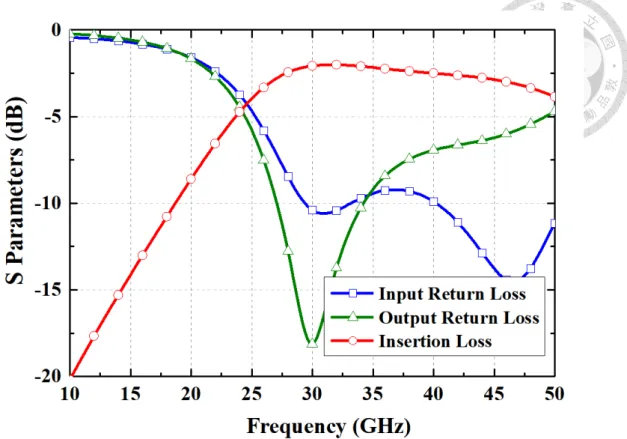
Fig. 2.44 Simulated and measured S-parameters of the proposed continuous Class-F-1 PA... 49
Fig. 2.45 Measured and re-simulation S-parameters of the proposed PA. ... 49
Fig. 2.46 Measured and simulated power performance of the PA at 33 GHz. ... 50
Fig. 2.47 Measured and simulated power performance of the PA at 38 GHz. ... 51
Fig. 2.48 The simulated and measured power performance of the proposed continuous Class-F-1 PA from 30 to 40 GHz ... 51
Fig. 2.49 (a) The measured modulation results with the single carrier 64-QAM signals of 100/200/400 MSymbol/s at 32 GHz. (b) Measured constellation diagrams and (c) Waveforms of the 64-QAM 400 MSymbol/s at 32 GHz. ... 53
Fig. 2.50 (a) The measured modulation results with the single carrier 64-QAM signals of 100/200/400 MSymbol/s at 38 GHz. (b) Measured constellation diagrams and (c) Waveforms of the 64-QAM 400 MSymbol/s at 38 GHz. ... 54
Fig. 2.51 (a) Measured constellation diagrams and (b) Waveforms of the single carrier 256-QAM signals 100 MSymbol/s at 32 GHz. (c) Measured constellation diagrams and (d) Waveforms of the single carrier 256-QAM signals 100
MSymbol/s at 38 GHz. ... 55
Fig. 2.52 (a) The measured modulation results with the 64-QAM OFDM signals of 100/200/400/800/1000 MHz bandwidth at 32 GHz. (b) Measured constellation diagram and (c) Waveform of the 64-QAM OFDM with a bandwidth of 400 MHz at 32 GHz. ... 57
Fig. 2.53 (a) The measured modulation results with the 64-QAM OFDM signals of 100/200/400/800/1000 MHz bandwidth at 38 GHz. (b) Measured constellation diagram and (c) Waveform of the 64-QAM OFDM 400 MHz bandwidth at 38 GHz. ... 57
Fig. 2.54 The measured modulation results with the 64-QAM OFDM signals of 400 MHz bandwidth from 30 to 40 GHz. ... 58
Fig. 3.1 Relationships among various power level in a two-tone test. ... 66
Fig. 3.2 Calculated calibration signal SNDR of a 39 GHz 64-elements phased-array transceiver. ... 66
Fig. 3.3 The simulated third-order transconductance of the MGTR. ... 68
Fig. 3.4 Schematic of the proposed Gilbert-cell mixer. ... 69
Fig. 3.5 Schematic of the double balanced mixer core. ... 70
Fig. 3.6 DC-IV curves of LO switching core. ... 71
Fig. 3.7 Simulated CG and output power versus different IF input power for different Vd at 28 GHz. ... 71
Fig. 3.8 Simulated conversion gain versus different LO power for different bias at 38 GHz. ... 72
Fig. 3.9 Simulated conversion gain versus LO power for different transistor fingers
at 38 GHz. ... 73
Fig. 3.10 Simulated LO port input impedance at different LO power at 38 GHz. ... 73
Fig. 3.11 The Id versus Vgs with different gate width. ... 74
Fig. 3.12 Simulated conversion gain of active mixer versus different LO power at 38 GHz. ... 74
Fig. 3.13 The EM layout of the LO matching network. ... 76
Fig. 3.14 The impedance seen before and after the LO matching circuit under different LO power at 37 GHz. ... 76
Fig. 3.15 The simulated insertion loss and I/O return loss of the EM LO matching network. ... 77
Fig. 3.16 The simulated insertion loss of transmission line of 28, 65, and 90 nm CMOS technology. ... 77
Fig. 3.17 The CG of the mixer core with and without LO matching network. ... 78
Fig. 3.18 The phase difference of the LO transformer design. ... 78
Fig. 3.19 The EM layout of the RF matching network. ... 79
Fig. 3.20 The impedance of the RF matching circuit from 10 to 50 GHz. ... 80
Fig. 3.21 The schematic of the transconductance stage with IM2 signal injection circuit. ... 81
Fig. 3.22 The small signal equivalent circuit of IM2 generator. ... 83
Fig. 3.23 The small signal equivalent circuit of IM2 generator for even harmonic signal. ... 83
Fig. 3.24 The small signal equivalent circuit of IM2 generator for IF input signal... 83
Fig. 3.25 The block diagram of proposed IM3 cancellation technique. ... 84 Fig. 3.26 The transconductance, the first and second order derivative of the
transconductance at different bias. ... 85 Fig. 3.27 Simulated two-tone IM3 and fundamental versus input power of the proposed mixer. ... 86 Fig. 3.28 The simulated CG versus LO power with 1.0 GHz IF frequency and 27 GHz LO frequency. ... 88 Fig. 3.29 Simulated performances versus RF frequency with LO power of 2 dBm and IF frequency of 1 GHz. ... 89 Fig. 3.30 Simulated performances versus IF frequency with LO power of 2 dBm and LO frequency of 27 GHz. ... 89 Fig. 3.31 The conversion gain and output power versus IF power. ... 90 Fig. 3.32 Simulated results of CG and output power at 28 GHz under different value of Vg1. ... 90 Fig. 3.33 The simulated two-tone signal measurement result at RF frequency at 28 GHz 25 MHz. ... 91 Fig. 3.34 The simulated two-tone signal measurement result at RF frequency at 28 GHz 250 MHz. ... 91 Fig. 3.35 Chip photo of the proposed mixer with a chip size of 0.79×0.61 mm2. ... 92 Fig. 3.36 The measurement setup of the up-conversion mixer. ... 95 Fig. 3.37 The measured and simulated CG versus LO power with LO frequency of 27 GHz, and IF frequency of 1.0 GHz... 95 Fig. 3.38 The capacitance of lateral flux capacitor and interdigital capacitor used in the LO transformer circuit. ... 96 Fig. 3.39 The measured and re-simulated CG versus LO power with LO frequency of 27 GHz, and IF frequency of 1.0 GHz after considering the discrepancy in LO port matching. ... 96
Fig. 3.40 The measured and re-simulated CG versus LO power with LO frequency of 27 GHz, and IF frequency of 1.0 GHz after considering the process variation in poly resistors. ... 97 Fig. 3.41 Schematic diagram of the parasitic effects in implementation. ... 97 Fig. 3.42 The measured and re-simulated CG versus LO power with LO frequency of 27 GHz, and IF frequency of 1.0 GHz after considering all of the unexpected factors. ... 98 Fig. 3.43 The simulated and measured CG versus RF frequency with LO power of 2 dBm and IF frequency of 1 GHz. ... 98 Fig. 3.44 Measured and simulated CG versus IF frequency with LO power of 2 dBm and LO frequency of 27 GHz. ... 99 Fig. 3.45 Measured and re-simulated CG versus IF frequency with LO power of 2 dBm and LO frequency of 27 GHz. ... 99 Fig. 3.46 The measured LO leakage versus RF frequency of the proposed mixer. ... 100 Fig. 3.47 The simulated and measured CG, output power versus IF input power at RF frequency of 28 GHz. ... 100 Fig. 3.48 The two-tone measurement result of RF power versus IF power at RF frequency of 28 GHz 5 MHz. ... 101 Fig. 3.49 The measured IMD3 result at RF frequency of 28 5 MHz with and without linearizer. ... 101 Fig. 3.50 The measured IMD3 result at RF frequency of 28 12.5 MHz with and without linearizer. ... 102 Fig. 3.51 Measurement setup of the modulated signal. ... 103 Fig. 3.52 (a) Measured constellation diagram and (b) Waveforms of the single carrier 64-QAM signals with 50 MHz baud rate upon linearizer turning on. (c)
Measured constellation diagram and (d) Waveforms of the single carrier 64-QAM signals with 50 MHz baud rate upon linearizer turning off. ... 104 Fig. 3.53 The measured EVM (dB) versus Pout (dBm) with and without linearizer of the 64 QAM 50 MHz Baud signal. ... 105 Fig. 3.54 (a) Measured constellation diagram and (b) Waveforms of the single carrier 256-QAM signals with 20 MHz baud rate upon linearizer turning on. (c) Measured constellation diagram and (d) Waveforms of the single carrier 256-QAM signals with 20 MHz baud rate upon linearizer turning off. ... 106 Fig. 3.55 The measured EVM (dB) versus Pout (dBm) with and without linearizer of the 256 QAM 20 MHz Baud signal. ... 106 Fig. 3.56 Constellation versus signal different distortion. ... 108 Fig. 3.57 Simulated AM-PM distortion of the device in the transconductance stage of proposed mixer at different input power level. ... 109
LIST OF TABLES
Table 1.1 Comparison of recently published mm-Wave PA. ... 4 Table 1.2 Modulation performance summary of published mm-Wave CMOS PA. ... 5 Table 1.3 Performance summary of the published up-conversion mixers and transmitter. ... 7 Table 2.1 Design targets of the proposed power amplifier. ... 15 Table 2.2 Load-pull simulation of different conditions of the same total device size. . 20 Table 2.3 The bias conditions of the proposed PA under quiescent condition. ... 47 Table 2.4 Modulation measured results with different modulation scheme at 32 GHz.59 Table 2.5 Modulation measured results with different modulation scheme at 38 GHz.59 Table 2.6 Comparison of the published 5G mm-Wave CMOS PAs. ... 62 Table 2.7 Modulation performance summary of published mm-Wave CMOS PA. ... 63 Table 3.1 Comparison of the previous published up-conversion mixers and transmitters. ... 112
Chapter 1 Introduction
1.1 Backgrounds and Motivations
Nowadays, fifth-generation (5G) cellular systems which will be able to provide higher data rates and less time latency become more and more close to people’s life.
Moreover, to relief the crowded spectrum below 6 GHz, the millimeter-wave (MMW) frequency bands of 30-300 GHz is one of the best solutions because extensive spectrum currently exists with light use. The mm-Wave spectrums of 28 GHz and 38 GHz bands are the most popular bands for 5G wireless technologies due to less absorbed during the wireless transmission in the air. The global standard (Release 15, 16) had been established for 5G systems by 3GPP [1]. Besides, most countries have been working hard on carrying out the 28 GHz wireless phased-array transceiver. Therefore, the 38 GHz band will be the next targeted frequency band, where can provide higher data capacity.
Although operating at the mm-wave frequency can provide a wider spectrum bandwidth, the dramatically attenuation is a critical problem due to the absorption by the air and traveling through the obstacles. To overcome this problem, the signal-to-noise ratio (SNR) and equivalent isotropically radiated power (EIRP) of the system have to be enhanced. A phased-array is the most hopeful applicant due to the inherent characteristics of antenna beam-steering and providing improvements in radiated SNR and EIRP which is related to the number of elements. Based on the previous work, a 64-element 28 GHz phased-array transceiver can demonstrate wireless communication with 64-QAM modulation signal at a link distance of 300 m which requires above 42 dBm EIRP from the link budget of 300 m 5G link [2]. Therefore, the requirement on the saturated output power of the power amplifiers in each element of
the phase-array system is more flexible. According to the recent study, the saturated output power around 16 dBm is the most common target [3],[4],[6],[44],[45]. Besides, high efficiency, broadband power performance, and back-off efficiency enhancement become the attractive study subject. Efficiency plays an important role in the improving battery life of portable devices and thermal management. To cover the wideband channels with compact elements in the mm-Wave transmitter, a broadband PA is more attractive than using several single-band power amplifiers [3]-[6],[11]. In the transmitter, power amplifier is the most decisive component that directly affects the linearity of the system. To sum up, high efficiency, good linearity, and wide band performances are the most important issue for the design of power amplifier [4]-[6],[19],[46]-[48].
To achieve high data rate wireless transmission, the communication system is proceeding towards high-level QAM modulation with high peak-to-average power ratios (PAPRs) and linearity requirement. For the transceiver, the mixer converts the baseband data up to MMW frequency and drives the power amplifier in the next stage.
However, when the input power becomes larger, the intermodulation distortion degrades the overall linearity of the mixer which is the main factor of the SNR in the high power region. Besides, the noise due to white noise, image signal, LO leakage signal, and interface from other transceiver dominates the SNR in the low input power region. For the high order QAM modulation, it desires higher SNR to support the same bit error rate.
As a result, the cancellation of IM3 distortion plays an important role to improve the modulation output power. In MMW up-conversion mixer, to take good care of conversion gain, LO power requirement, isolation, and isolation is still an important work.
1.2 Literature Survey
1.2.1 Broadband and High Efficiency Power Amplifier
To satisfy the ever-growing demand of 5G communication for high data rates, the millimeter-wave (mm-Wave) transceiver is expected to achieve a wide spectrum bandwidth. Moreover, power amplifiers with high efficiency are a beneficial on the thermal handling and the power consumption of the system. To meet these requirements, implementation of power amplifiers with high peak efficiency and wide output power bandwidth has become a critical research topic. Besides, study on the linearity of power amplifier is also a challenging research topic. To increase the data rates, OFDM modulation is one of the possible solutions which has more critical requirement on the linearity. Table 1.1 shows the comparison of the recent publications of mm-Wave CMOS PAs. There are many techniques adopted to enhance the peak efficiency or the bandwidth in mm-Wave PA design. Transformer matching which considered as the high-order matching circuit is one of the most common method for broadband design [3],[22],[23]. Reference [3] reports a broadband PA work fabricated in 65 nm CMOS technology which provides saturated output power of 15.3 dBm and discusses the design of transformer matching with uncoupled resonant frequency, Q factor, and peak impedance. However, the bandwidth with the peak PAE above 30 % only covers from 24 – 32 GHz which shows degradation from the 3-dB S21 bandwidth from 22 – 42 GHz.
Recently, the harmonic-tuned PAs are one of the solution to enhance the peak efficiency [4],[5],[18],[21]. Moreover, the modulation performances of the published PAs are listed in Table 1.2. There are several linearization techniques, which is realized by adding PMOS, varactors, or second harmonic termination [12],[18],[22]. Since these techniques are designed on the chip with the PA, no external implementation is required.
In reference [18], it demonstrates that the IM3 distortion which caused by the common mode feedback of the neutralization capacitors can be improved with the second harmonic matching. Furthermore, the AM-AM and AM-PM distortion can be improved with the two-step second harmonic termination. Although several mm-Wave PAs based on class-F or inverse class-F (class-F-1) have outstanding performance, the high efficiency is achieved over a limited bandwidth. Moreover, in references [4] and [21], these PAs require several inductors and capacitors to achieve the proposed harmonic matching which generates additional insertion loss. Therefore, it is challenging to achieve high peak efficiency and broadband simultaneously based on reported broadband PA designs in recent years.
Table 1.1 Comparison of recently published mm-Wave PA.
Ref. Process Topology Freq.
(GHz)
Gain (dB)
Psat
(dBm)
OP1dB
(dBm)
PAEpeak
(%)
> 30%
PAEpeak
BW (GHz)
Chip Area (mm2)
IMS’16
[21] 0.13-m SiGe
2-stage
CF-1 CS 39-42 22 18 16 43 38-43* 0.57
RFIC’17 [22]
28-nm CMOS
2-stage DE CS with
APD
29-57 20.8 16.6 13.4 24.2 x 0.32
MWCL’18
[23] 90-nm
CMOS 2-stage
Doherty 29-42 19.8 20.7 18.5 32.7 32-36* 0.21 TCAS’18
[3] 65-nm
CMOS 2-stage CS 22-42 20.8 15.3 12.9 32.9 24-32* 0.11 IMS’19
[12]
65-nm
CMOS 2-stage CS 39 14.4 20.7 20.2 35 38-40 0.21
TMTT’19 [5]
45-nm CMOS SOI
2-stage CCF/CCF-1
Cascode
23.5-41 11.4 18.6 16.6 45.7 25.5-41* 0.14
TCAS’19
[4] 65-nm
CMOS 1-stage SE
CCF CS 25-35 10 14.7 13.2 46.4 25-35 0.12
RFIC’19
[18] 28-nm
CMOS 2-stage
Cascode 37-40 25.8 16.8 14.9 32.9 37-40 0.07 (core area)
Table 1.2 Modulation performance summary of published mm-Wave CMOS PA.
Ref. Process
Freq.
(GHz)
Modulation Scheme
Data Rate
(Gb/s) EVM (dB)
Po,avg
(dBm)
PAEavg
(%) RFIC’17
[22] 28-nm
CMOS 34 64-QAM 1.5 -25# 10.1 5.8
MWCL’18
[23] 90-nm
CMOS 34 64-QAM 3 -27.4# 11.1 5.1
IMS’19 [12]
65-nm
CMOS 38 64-QAM
OFDM 5.76 -25* 13.2 7.1
TMTT’19 [5]
45-nm
CMOS SOI 39 64-QAM 3 -28.1* 11 10.2
TCAS’19
[4] 65-nm
CMOS 34 64-QAM 1.5 -25.9* 8.6 21.4
RFIC’19
[18] 28-nm
CMOS 38.5 64-QAM
OFDM 5.04 -25* 10.3 16.9
# Normalized by average power (EVMrms), * Normalized by peak power (EVMmax)
1.2.2 High Linearity Up-Conversion Mixer
To achieve high speed wireless data transmission, the millimeter-wave (mm-Wave) transceiver achieves this requirement by both wide spectrum bandwidth and using high-order QAM modulation signal which needs a harsh requirement on the linearity of the system. In a wireless communication system, linearity is one of the most important specifications of the mixer. Active mixer can provide higher conversion gain with lower LO power but demonstrate poor linearity compared with passive mixer. Furthermore, the IM3 distortion plays an important role in the SNR when transmitter is operated in the high power region. To enhance the linearity of the mixer, several linearization techniques are applied, and Table 1.3 summarizes the published up-conversion mixers and transmitters. The previous work [41] demonstrates an up-conversion mixer which provides an output 1-dB compression point (OP1dB) of -6.2 dBm and third-order intercept point (OIP3) of 13.6 dBm. Nonetheless, the linearization technique is carried out at 10 GHz. At mm-Wave frequency bands, it is difficult to use the same method to improve the linearity. There are many techniques used to enforce the linearity of mixer
in the MMW frequency [6],[28]-[32],[39]. Multiple gate transistors (MGTR) [28]-[30]
and distributed derivative superposition (distributed DS) [31],[32] are the techniques to cancel third-order intermodulation (IM3) current which are originally developed for the LNA. The ideas utilize several parallel transistors with various sizes and bias condition to cancel the third-harmonic signals. Reference [32] presents a 38-54 GHz up-conversion mixer which provides a conversion gain of -2.5 dB and third-order intercept point (OIP3) of 4 dBm. Splitting cascode topology is the other approach that has a dramatic cancellation of IM3 distortion [39]. The proposed topology consists of two paths with different bias condition in the transconductance stage. This work shows the outstanding OIP3 of 32 dBm with dc power of 154.4 mW and possesses two sweet-spots of IM3 according to the two-tone measurement results. However, all of the approaches mentioned above require specific bias conditions for the main and auxiliary transistors to cancel third-harmonic signals. Furthermore, the improvement of IM3
distortion is impressive in the low power region among those works. Therefore, to compare with the published mixers and transmitter, linearity improvement is desired for high data rates 5G communication. Moreover, the IM3 cancellation in the wide IF power region is still a hot topic.
Table 1.3 Performance summary of the published up-conversion mixers and transmitter.
Ref.
[40]
2009 TMTT
[41]
2019 TMTT
[32]
2019 RFIT
[39]
2019 IMS Process 0.15 m
InGaAs
32 nm
CMOS SOI 65 nm
CMOS 65 nm
CMOS
Topology Gilbert cell
Up-conversion mixer with harmonic nulling
Gilbert cell with derivative
superposition
Transmitter
RF Freq.
(GHz) 15 10 38-54 39.5-40.5
CG.
(dB) 5 1 -2.5 19
LO power
(dBm) 10 N/A 5 8.5
OP1dB
(dBm) -6 -6.2 -11.7 13
OIP3
(dBm) 8 13.6 4 32
DC Power
(mW) 86.4 15.4 8.5 154.4
1.3 Contributions
This thesis presents a 30-40 GHz high efficiency and wideband CMOS power amplifier, and a 28-GHz high linearity up-conversion mixer. The contributions of these works will be introduced as following.
1.3.1 30-40 GHz Broadband and Efficiency CMOS PA
A 30-40 GHz high efficiency and broadband power amplifier with continuous mode harmonic-tuned output network using 65-nm CMOS process is proposed. The advantage of continuous harmonic-tuned output matching is that the efficiency can be enhanced in the wide bandwidth through rectifying the current and voltage waveform.
Moreover, unlike the class F/F-1 power amplifier which requires the specific harmonic impedance matching, continuous mode PA exhibits the same output performance with multiple impedance solutions and a family of current or voltage waveform. Thus, we propose a specific method to design the output matching circuit at different order harmonic frequency. Moreover, this work demonstrates the detail analysis of harmonic matching network using the parasitic elements of the transformer in the desire frequency band. Since the bias condition of the transistors would influence the linearity of the power amplifier, this work provides the detail analysis and shows that power amplifier with harmonic-tuned output matching circuit can improve the AM-PM distortion.
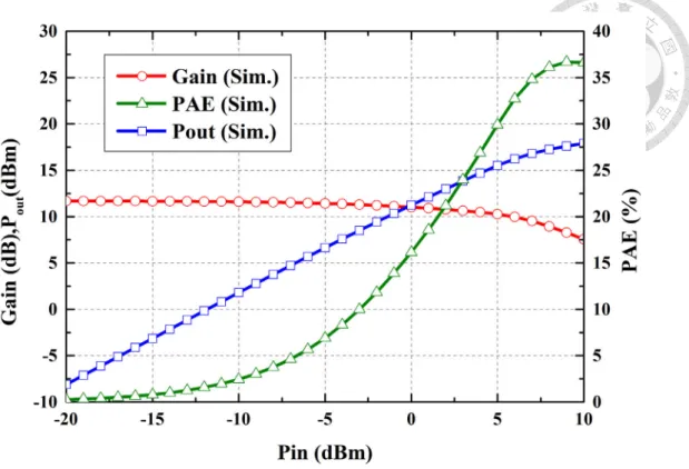
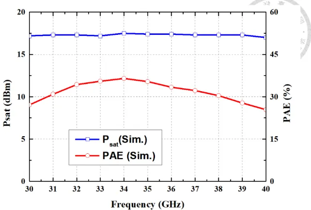
Thanks to these design feature, the proposed PA shows a small-signal gain of 11.7 dB, a saturated output power (Psat) of 17.9 dBm, output power bandwidth (30 to 40 GHz) with 33 % peak PAE, and output 1-dB compression point (OP1dB) of 15.0 dBm at 34 GHz.
When tested with a single-carrier 64-QAM signal, this PA achieves bandwidth of 400 MHz, 14.1-dBm average output power, and 22.1% average PAE under root-mean-square (rms) error vector magnitude (EVM) -25.1 dB. Among all the published mm-Wave CMOS PAs, this PA shows outstanding large-signal performances and exceptional modulation capability. This work has been published in 2020 RFIT [42].
1.3.2 28-GHz CMOS up-conversion mixer
In this thesis, a 28-GHz high linearity up-conversion mixer in 28-nm CMOS technology is demonstrated. The third-order intermodulation signal is the main interference on the signal-to-noise and distortion ratio (SNDR) in the high input power region. However, the previous mixers like derivative superposition technique which is developed for LNA only works at low power region. As a result, to cancel the IM3
distortion across a wide IF power region, the proposed mixer adopts the structure of double-balanced active mixer with an IM2 signal injection technology at the transconductance stage. The second-order intermodulation (IM2) injection is the technique which produces the positive IM3 current to improve the distortion [33]-[36].
Nonetheless, the previous works were carried out in the low frequency [33] or only analyzed by Volterra series analysis without measurement result [34]-[36]. To the best of author’s knowledge, this design is the first demonstration and implemented of an IM2
signal injection technique in millimeter-wave frequency. Moreover, we analyze IM3
distortion, the AM-AM, and AM-PM distortion of the up-conversion mixer. With the modulation measurement results using the single-carrier QAM signals, we can verify our study by the constellation diagram. Due to these design features, the proposed mixer demonstrates a conversion gain (CG) of -6.4 dB and output 1-dB compression point (OP1dB) of -2.2 dBm with 19 mW. The two-tone measurement results exhibit an explicit IM3 distortion improvement and achieves 10.2 dBm output third-order intercept point (OIP3). Furthermore, with the modulation measured results using single-carrier 256-QAM signal, the proposed mixer also exhibits a distinguished output power enhancement when the linearizer turns on. This work has been published in 2021 MWCL [43].
1.4 Thesis Organization
The organization of the thesis is outlined in this section. In Chapter 2, a 30 – 40 GHz high efficiency continuous Class-F-1 power amplifier in 65-nm CMOS technology is presented. At first, the device size and bias selection are optimized for the design goal.
Then, the differential amplifier with capacitive neutralization technique is utilized to
enhance the stability of the transistors. The discussion of harmonic-tuned output matching will be given, as well. Besides, the improvement of AM-PM distortion in the proposed PA is demonstrated and explained. The measured results are displayed in 2.3.
In the end, the proposed circuit is compared with other published works in 2.4. A short conclusion is presented at the end of this chapter.
The design of a high linearity 28-GHz up-conversion mixer in 28-nm CMOS technology is proposed in Chapter 3. First, the size of the mixer core and transconductance is analyzed refer to the conversion gain of the mixer. The proposed IM3 signal generated from IM2 signal generation circuit and the transconductance stage are discussed in this part. The measured results are displayed in 3.3. In the end, the proposed circuit is compared with other published works in 3.4. A short conclusion is presented at the end of this chapter. Finally, Chapter 4 is the conclusion of this thesis.
Chapter 2 A 30-40 GHz Power Amplifier with Continuous Class F
-1matching in 65 nm CMOS Technology
This chapter presents a continuous-mode inverse Class-F (i.e., Class-F-1) power amplifier design to achieve both high efficiency and wide bandwidth performance for 5G wireless communications. With the proposed harmonic matching, this PA attains both broadband power performance and linearity improvement. To reduce the harmonic load complexity and insertion loss, the proposed fundamental and harmonic matching for continuous inverse class-F operation are achieved using the output transformer with an embedded inductors and capacitors. According to the measurement result, the proposed continuous Class-F-1 PA shows a saturated output power (Psat) of 17.9 dBm, output power bandwidth (30 to 40 GHz) with 35.8 % peak PAE, and output 1-dB compression point (OP1dB) of 14.4 dBm at 33 GHz. When tested with a single-carrier 64-QAM signal, this PA achieves bandwidth of 400 MHz, 14.1-dBm average output power, and 22.1% average PAE under root-mean-square (rms) error vector magnitude (EVM) -25.1 dB. Among all the published mm-Wave CMOS PAs, this PA shows outstanding large-signal performances and exceptional modulation capability.
2.1 Introduction
Driven by the ever-growing demand of 5G communication for high data rates, the millimeter-wave (mm-Wave) transceiver is expected to achieve a wide spectrum bandwidth. Since the power amplifiers (PA) are the last building block of transmitter, design of the applicable PA plays a dominant role. To cover the wideband channels with compact elements in mm-Wave transmitter, a broadband PA is more attractive than
using several single-band power amplifiers. Moreover, a high-efficiency PA is needed to enhance thermal handling and reduce the power consumption of the system. To meet these requirements, implementation of power amplifiers with high peak efficiency and wide bandwidth has become a critical research topic [3]-[6].
Recently, there are many techniques adopted to enhance the peak efficiency or the bandwidth in mm-Wave PA design. In [7], the negative resistance technique is used to enhance power performance of the PA which sacrifices stability of the circuit. Therefore, this technique is more suitable for power amplifier operating in V-band. Furthermore, harmonic-tuned PA, including Class-F and inverse Class-F, is another candidate for realizing high efficiency. For Class-F output matching circuit, it is required to provide open-circuit (O.C.) terminations at odd harmonics and short-circuit (S.C.) terminations at even harmonics. Similarly, for Class-F-1 output matching circuit, it is needed to show S.C. terminations at odd harmonics and O.C. terminations at even harmonics. Thus, a square voltage/current waveform is shaped, which has no overlap with the half-sinusoidal current/voltage for Class-F/F-1, leading to a theoretical 100% efficiency.
However, harmonic control is usually conducted up to the third order, as further harmonic control yields limited efficiency improvement and significantly increases implementation difficulty. In [8], when the supply voltage becomes higher, the efficiency of the Class-F-1 amplifier is better than that of the Class-F amplifier due to the higher peak voltage to knee voltage ratio to maintain an identical output power.
However, these PA modes require multiple accurate harmonic terminations which is hard to conduct in the wide bandwidth. As a result, the continuous Class-F/F-1 PA are the other impedance solutions that can be dynamically distributed over the desired bandwidth and generate a family of voltage/current waveforms, while maintaining the expected output power and efficiency.
Phase (Degrees)
Volt age Wave for m
0 180 360 540 720
Cu rre n t W av ef or m
ζ = 0 ζ = -0.5
ζ = -1 ζ = 0.5 ζ = 1
Fig. 2.1 Voltage and current waveforms of the continuous Class-F-1 mode.
For the continuous Class-F-1 mode, the current waveform can be extended by modifying the current waveform as follows [9]:
1( ) (DC 1cos 3cos3 ) (1 sin ).
iCF i i i (2.1)
In equation (2.1), the caseζ= 0 corresponds to the standard Class-F-1 mode and the possible range ofζis from -1 to 1. Therefore, there are a family of current waveforms that offer a continuous design space with constant output performance theoretically in the range of proposed frequency band. The continuous Class-F-1 PA can be realized over the desired bandwidth by applying the required harmonic impedances for differentζ, which can be determined from the conductance calculated using the equation (2.1) as follows:
Fig. 2.2 Continuous inverse Class-F in the admittance chart.
1
1
1
1
1 3
2, 3,
2 2
2( )
opt opt DC
F F opt F
Y G i jG i
Y jG i i
Y
(2.2)
where Gopt = 1/Ropt. The calculated harmonic loads of continuous Class-F-1 mode are shown in Fig. 2.2 with -1 ζ 1.
In this chapter, a 30 to 40 GHz continuous class-F-1 PA fabricated in 65-nm CMOS process is presented. In order to reduce the insertion loss and chip size, we propose a different harmonic-tuned network from that in [4]. With the proposed output matching, this work achieves high peak efficiency and broadband operation simultaneously.
Moreover, the harmonic-tuned matching also improves the AM/PM distortion of the proposed PA. Furthermore, the relation between AM/PM and bias selection is also discussed.
2.2 Circuit Design
The proposed 30-40 GHz PA with continuous Class-F-1 output matching is designed in TSMC 65-nm CMOS process with one poly layer, nine copper (Cu) metal layers, and two metal-insulator-metal (MIM) capacitor layers. The threshold voltage of the transistor in this process is roughly 0.3 V. The suggested maximum supply voltage of the transistor in this process can be 1.2 V with 5% tolerance and normally 1.0-V suggested by the foundry. In this work, the proposed power amplifier is designed with 1.2-V supply voltage for higher output power and power added efficiency (PAE). The design targets of the proposed power amplifier are listed in Table 2.1. The target frequency is from 30 to 40 GHz with small signal gain of 10 dB. The I/O return losses are set to be higher than 5 dB. In the recently works, the 5G phase-array communication systems are composed of numerous radiating elements with a phase shifter and PA/LNA for each one. As a result, power amplifier with a saturated output power of 15 to 18 dBm and higher PAE is more suitable for phase-array communications in the recently work. The target output saturated power (Psat) is set to about 18 dBm with PAE of 35 %.
Table 2.1 Design targets of the proposed power amplifier.
2.2.1 Circuit Architecture
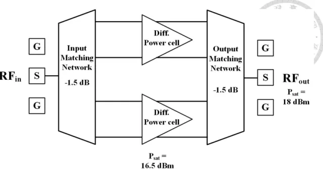
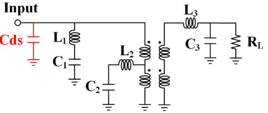
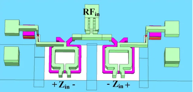
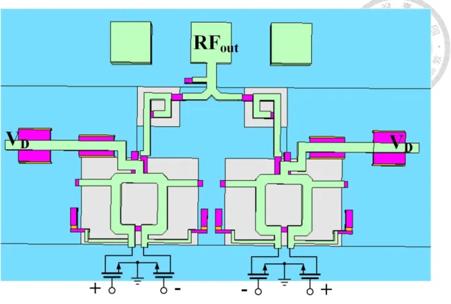
The circuit architecture of the proposed power amplifier with continuous Class-F-1 output matching is shown in Fig. 2.3. This PA is composed of two differential common source amplifier cells. M1, M2 are consisted of four combing transistors for higher intrinsic PAE. Moreover, the cross-coupling neutralization is utilized to improve power gain, reverse isolation, and stabilize the amplifiers. For continuous mode power amplifiers, they need several passive elements to carry out the precise reactive load mapping at fundamental and harmonic bands which produces additional loss in the output matching. In the ideal circuit design, we propose a different harmonic-tuned network from that in [4]. This technique exploits and enhances the parasitic elements in a physical on-chip transformer to achieve continuous-mode harmonic tuning with substantial area-reduction. By the proposed output matching, this work achieves high efficiency and broadband power performance simultaneously.
Fig. 2.3 Circuit Architecture of the proposed power amplifier.
Fig. 2.4 The block diagram and power budget of the proposed PA.
2.2.2 Device and Bias selection
The block diagram and power budget of this PA are shown in Fig. 2.4. The input/output matching network are realized by transformers. In the initial power budget, the estimated insertion loss of matching network is assumed to be 1.5 dB. Therefore, the saturated output power of each power cell should be higher than 16.5 dBm. In the power amplifier design, selection of device size is directly related to the target output power.
From the load-line theory [10], the output saturated power of the PA can be expressed as the following:
max min max
1
2 2 2 4
pp k
sat D
V V
V V I
P I (2.3)
where Vpp is the peak to peak output drain voltage and Vk is the knee voltage of the transistor. The DC-IV curve versus different gate bias is shown in Fig. 2.5. In 65-nm CMOS process, the supply voltage of the transistor is 1.2 V and the maximum recommended AC voltage swing (Vpp) is twice of dc supply voltage. Furthermore, the Vk
is the threshold voltage which is about 0.3 V in the 65-nm CMOS technology, as shown
in Fig. 2.5. Because the proposed PA is designed for Class-F-1 operation, the gate bias voltage (Vgs) should be selected at Class-C operation. However, the bias selection is also related to the AM/PM distortion of the power amplifier design. Moreover, the detailed analysis will be discussed in this part. As a result, the operating condition of the proposed PA is decided at deep Class-AB. For a target Psat of 16.5 dBm (44.67 mW), a total dc current of 85.1 mA can be calculated in the Class-AB operation (Vg 0.6 V). Fig.
2.6 demonstrates the curve of transistors with different gate width per 32 fingers.
According to this figure, the current density of the device is roughly 0.28 mA/m in the same biasing region. As a result, the total gate width of is 358 m determined for the power stage design.
Fig. 2.5 The DC-IV curve versus different gate bias with the device of 64-m total gate width.
Fig. 2.6 The Id versus Vgs with different gate width
For the total gate width of 358 m, choosing multi-finger and multi-way combing transistors is commonly used to decrease the intrinsic gate resistance with the same total device size. Table 2.2 compares the load-pull simulations of a differential power cell which consist of different finger, gate width per finger, and numerous of transistors with the same total size. The results show that combining more transistors and using more fingers of the device can reach better performance of intrinsic peak PAE with roughly the same Psat. Nonetheless, the input impedance of amplifier would become smaller due to shunting all of the input conjugate impedance by combing numerous devices. As a result, it places large burden on the design of input matching network. To sum up, each differential power cell is built by combing four transistors as a unit and each size of transistors is 1.4 m × 32 fingers.
Table 2.2 Load-pull simulation of different conditions of the same total device size.
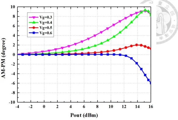
For continuous Class-F-1 PA design, the bias condition should be chosen at closed to Class-B operation. However, bias voltage is one of critical parameters for the power amplifier design. Simulated PAE with different Vg at different output power levels is shown in Fig. 2.7. For the transistors biasing at deep Class-AB mode, higher back-off efficiency is demonstrated compared with the device biasing at Class-A due to smaller dc drain current at the low power region. Therefore, the bias condition of this PA is chosen at 0.4 V to exhibit higher PBO efficiency. However, the AM-AM and AM-PM distortions are also related to bias condition of the power amplifier. The AM/AM distortions versus Vgs with different output power level at 38 GHz is shown in Fig. 2.8.
Thanks to the positive gm3 of the device, the transistor biasing at triode region exhibits superior AM/AM distortion compared with the transistor biasing at saturated region.
Although PA biased at 0.4 V demonstrates better PBO efficiency, a worse AM-AM distortion is also observed. Prior works [11],[12] show that the AM/PM distortion is related to the nonlinearity of input capacitance variation at different input power level.
The equivalent circuit of small signal transistor model is shown in Fig. 2.9. For the common source transistors, the parasitic elements at the gate can be considered as a first-order low-pass RC circuit. Since the parasitic capacitor Cgs depends on the Vgs of the device, the output current at the drain of transistors Iout can be expressed as follows
[27]:
2
( ) g ( ) cos( 2 ...)
2
g in IF IF
out m gs IF IF g in IF
R C V
I t V t V t R C
(2.4)
where 2 represents second-order voltage dependence of Cin. As a result, the phase of output current contains an input-dependent term which is related to the capacitance Cin. When the input power level becomes higher, the large variation of Cin will increase2 in the equation (2.4) which causes sever AM-PM distortion. Both parasitic capacitance Cgs and Cgd are main factor of input capacitance Cin. Gate to source parasitic capacitance Cgs versus different bias condition is shown in Fig. 2.10. The value of Cgs has higher variation around 0.3 V which will degrade AM-PM distortion of PA. Besides, there is an equivalent capacitance of (1-Av)×Cgd at the gate of the device owing to the Miller effect, where Av is voltage gain of the transistor. In the high input power region, output voltage will contain several harmonic distortion signals which leads to a severe nonlinearity of ttttt
Fig. 2.7 Simulated PAE with different Vg at different output power levels.
Fig. 2.8 AM/AM distortions versus Vgs with different output power level.
Fig. 2.9 The equivalent circuit of small signal transistor model.
Fig. 2.10 Simulated Cgs at different bias condition.
Fig. 2.11 Cin versus output power with different bias condition.
Fig. 2.12 AM/PM distortions versus Vgs with different output power level.
(1-Av)×Cgd. Therefore, considering the above problems, input parasitic capacitance Cin
versus input power with different bias condition is shown in Fig. 2.11. Besides, Fig.
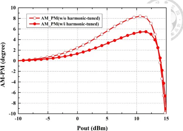
2.12 shows AM/PM distortion at different output power level under different bias condition. Device biasing at the Vgs of 0.5 V has smaller variation of input parasitic capacitance which causes lowest AM/PM distortion. There is an AM-PM distortion up to 8oof transistors biased at 0.4 V. In conclusion, this proposed PA is biased at 0.4 V to increase PBO efficiency, while also to degrade the AM-AM and AM-PM distortion of the PA.
2.2.3 Capacitance-Based Neutralization
The small signal equivalent circuit of a neutralized differential common source (CS) transistors is shown in Fig. 2.13. The existence of gate-to-drain parasitic capacitor Cgd
establishes a feedback path and degrades reverse isolation which becomes more severe
Fig. 2.13 The equivalent small signal model of a neutralized differential common-source transistor pair.
in the millimeter-wave frequency. Furthermore, to achieve the proposed saturated output power, the total device size of the transistors is large which makes the influence of Cgd
become more severe. The reverse isolation is directly related to S12. Furthermore, the MSG/MAG composed of S-parameters is equal to
21 12
21 2 12
( 1)
MSG S S
MAG S K K
S
(2.5)
where the increase of S12 will reduce the MSG/MAG of the transistor and cause the device to be more unstable. So, the capacitance-based neutralization technique with cross-coupled capacitors used to cancel the Cgd for differential CS has been adopted for a long time [13]. As shown in Fig. 2.13, the cross-coupled capacitors (CNEU) is applied between the gate and drain of the two CS device in differential operation, and gg, gds, gm, Cgs, Cgd are the equivalent parasitic gate conductance, drain-source conductance, transconductance of transistors and the parasitic capacitance. To investigate the stability consideration, the Rollett stability factor (K) is one of the effective tool. Unconditional stability of a two-port network is ensured when K factor greater than unity, Re{Y11} and Re{Y22} greater than 0. As a result, with the neutralized capacitor, Y-parameters and K
Fig. 2.14 The simulated K factor and maximum gain of the differential CS transistor pair with device of 358m total gate width versus different CNEU.
factor can be expressed as
11 12 21 22
(c c )
(c c )
(c c )
(c c )
g gs gd neu
gd neu
m gd neu
ds ds gd neu
Y g s c s
Y s
Y g s
Y g s c s
(2.6)
and
2 2
2 2 2
2 (c c )
( )
g ds gd neu
gd neu gd neu m
K g g
c c c c g
(2.7)
In (2.7), it demonstrates that the K factor of differential CS is highly improved when Cgd
equals to CNEU. Moreover the voltage gain of the device is also enhanced. Since the MAG of the transistors reaches maximum value when the K factor is unity, the value of CNEU is chosen a little higher than the value which gets the maximum of K factor.
However, excessive CNEU will lead to higher S12 and let the transistor become instable.
The simulated stability factor and maximum gain of differential CS with the device of 358 m total gate width versus different CNEU is shown in Fig. 2.14. Finally, the CNEU is chosen as 57 fF which will can be realized thought an interdigital capacitor.
2.2.4 Load-pull Simulation for Continuous Class-F-1 operation
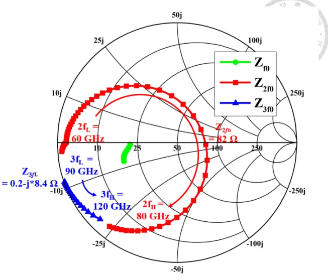
After deciding the transistor size and the bias condition, we can obtain the optimal load impedance (Zopt) to design the output matching network according to the load-pull simulation result. For the harmonic-tuned power amplifier, the drain-to-source parasitic capacitance (Cds) should be considered as one of the output matching elements to produce the proposed current waveform. As a result, the harmonic-tuned output matching network can be precisely designed with the known Cds. To get the capacitance of the Cds, an ideal negative capacitance is added to cancel out the Cds when doing the load-pull simulation. For the continuous mode operation, load-pull simulation at different frequency is conducted to ensure the Zopt in the proposed fundamental thettttttttt
(a)