The Other Crucial Factor Dominates the Holes Injection
Efficiency of Ultra-thin Anode Buffer Layer on Organic Light
Emitting Devices
Sheng-Yuan Chu
*, Yu-Cheng Chen
*, Hsin-Hsuan Huang
*and Po-Ching Kao
** *Department of Electrical Engineering, National Cheng Kung University, Tainan 70101, Taiwan**Department of Applied Physics, National Chiayi University, Chiayi 60004, Taiwan
ABSTRACT
In this study, we have investigated surface energy of
ITO substrates modified by ultra-thin buffer layers plays a crucial factor as important as energy barrier. With larger surface energy, organic light emitting devices could get superior performance even there exist larger barrier between ultra-thin buffer layer modified ITO and organic layer.
INTRODUCTION
Multilayer organic light-emitting diodes (OLEDs) have been considered as promising candidates for light-weight, fast-response, full-color displays ever since Tang and Van Slyke reported the first efficient OLED. In order to improve the efficiency, the insertion of a metal-oxide such as MoOx,
ZnO, or Fe3O4 has attracted a lot of attention due to its
capability to lower the hole-injection barrier to increase efficiency. However, each attempted buffer material reported explained by forming the dipole at interface and then bending energy diagram to decrease the injection barrier. Here we adopting two buffer layer materials elucidate the surface energy plays a crucial role for holes injection efficiency as important as energy barrier. The results show that the work function is not the exclusive factor in determining the hole-injection efficiency. Surface energy plays dominating role as well.
EXPERIMENTS
Prior to film deposition, the ITO glass substrate was cleaned sequentially with a neutraler reiniger/deionized water (1:3 volume) mixture, deionized water, isopropanol and ethanol, followed by UV-ozone treatment (Jetlight UVO-42) for 20 min. Device structure was ITO/buffer layer/NPB(40 nm)/Alq3(40 nm)/LiF(1 nm)/Al(100 nm). The current density-voltage (J-V) and luminance-voltage (L-V) characteristics were measured with a source meter (Keithely-2400) and a luminance meter (LS-100). NaF and CuF2 were adopted as ultra-thin buffer layer; their
optimized thickness has been found and adopted on following experiments. The UPS (ultraviolet photoelectron spectroscopy) and high resolution XPS (X-ray photoelectron spectroscopy) measurements were performed in air with Riken Keiki AC-2 and Kratos Axis Ultra DLD with a monochromatic Al Kα (1486.6 eV)source, respectively. The contact angle of ultra-thin films was measured using the Sessile drop technique with a Contact Angle Goniometer (MagicDrop, USA) under ambient conditions. The surface energy was estimated from the
measured contact angles using the following geometric-mean expression. 2 / 1 2 / 1
)
.
(
2
)
.
(
2
)
cos
1
.(
Sp Lp Sd Ld Lθ
γ
γ
γ
γ
γ
+
=
+
where γL (= γLp + γLd) and γS (= γSp + γSd) are the surface tension of the test liquid and the surface energy of the solid, respectively.
RESULTS and DISCUSSIONS
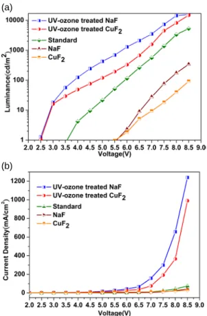
Figure1 shows the current density-voltage and luminance-voltage characteristics of the OLEDs with a pristine or a UV-ozone treated buffer layer deposited
between the ITO substrate and hole-transporting NPB layer. Fig1 (a) and (b) reveals that the device performances i.e. luminance, current density and turn on voltage all are superior than standard device when buffer layers were treated by UV-ozone and get worse with pristine buffer layers.Figure2 shows the schematic relationship between photoelectron emission and incident photon energy for buffer layers deposited on an ITO substrate, pristine and after UV-ozone treatment, as measured by a photoelectron spectrometer (AC-2). It reveals ITO modified by CuF2 layer either UV-ozone
treated or pristine shows no barrier between electrode and organic but NaF layer does. Interestingly, the results of energy diagram are drastically different with the device performances. There must exit another crucial factor dominates the hole injection efficiency between buffer layer/ITO anode and organic layer.
As shown in Fig3, the surface energy of bare ITO substrate is 51.14mJ/m2; they decreased to 42.52,
38.82mJ/m2 when ITO is covered by pristine NaF and CuF2 layer, respectively. However, they significantly
increase to 72.22 and 67.65 mJ/m2 after UV-ozone
treatment. These results demonstrate that covering an ITO surface with UV-ozone-treated NaF or CuF2 thin
layer increases surface energy and the work function, which in turn improves the device performance. Without UV-ozone treatment, only the work function of the ITO is increased, which leads to inferior device performance even it has no energy barrier like CuF2/ITO anode. The
increase in surface energy of the NaF and CuF2 layer
after UV-ozone treatment may have resulted from its oxidation during the treatment. Thus the treated NaF and CuF2 layer contacts intimately with the hole-transporting
NPB layer to facilitate hole-injection. Our results demonstrate that the work function is not the exclusive factor in determining the hole-injection efficiency.
Surface energy plays dominating role as well.
CONCLUSION
How the surface energy of ultra-thin buffer layers has
been elucidated. Increasing the surface energy and the work function simultaneously causes superior performance of the OLEDs. Raising work function only without surface energy at the same time, even there is no barrier between ITO and the organic layer it still leads to inferior device performance. The results show the surface energy indeed another crucial factor that dominates the performance of OLEDs. It indeed a crucial factor should be considered when choosing the buffer layer materials.
REFERENCES
[1] C. W. Tang, and S. A. Van Slyke, “Organic electroluminescent diodes,” Appl. Phys. Lett. 51(12), 913–915(1987).
[2] C. W. Tang, S. A. Van Slyke, and C. H. Chen, “Electroluminescence of doped organic thin films,” J. Appl. Phys. 65(9), 3610–3616 (1989).
[3] H. You, Y. Dai, Z. Zhang, and D. Ma, “Improved performances of organic light-emitting diodes with metal oxide as anode buffer,” J. Appl. Phys. 101(2), 026105 (2007).
[4] H.-H. Huang, S.-Y. Chu, P.-C. Kao, Y.-C. Chen, M.-R. Yang, and Z.-L. Tseng, “Enhancement of hole-injection and power efficiency of organic light emitting devices using an ultra-thin ZnO buffer layer,” J. Alloy. Comp.479(1–2), 520–524 (2009).
[5] Z. Z. You, “Combined AFM, XPS, and contact angle studies on treated indium-tin-oxide films for organic light emitting devices,” Mater. Lett. 61(18), 3809–3814 (2007).
[6] Y. Chen, P. Kao, and S. Chu, “UV-ozone-treated ultra-thin NaF film as anode buffer layer on organic light emitting devices," Optics Express 18, 167-173 (2010).
[7] S. Zhan, X. Ying-Ge, L. Xia, and Y. Tao, “A novel hole-blocking layer NaF between the α-naphthylphenyliphenyl diamine and ITO,” Appl. Surf. Sci. 253(9), 4374–4376 (2007).
[8] J. S. Kim, R. H. Friend, and F. Cacialli, “Surface energy and polarity of treated indium–tin–oxide anodes for polymer light-emitting diodes studied by contact-angle measurements,” J. Appl. Phys. 86(5), 2774–2778 (1999).
(a)
(b)
Fig 1. (a)L-V (b)J-V characteristics for OLEDs with various ultra-thin buffer layers
Fig 2. Schematic energy diagram
Fig 3.Suface energy of ITO substrate and various ultra-thin buffer layers covered ITO substrates