國 立 交 通 大 學
電子工程系
碩 士 論 文
異常光學穿透現象於兆赫波段之研究
Study of Extraordinary Optical Transmission in THz Region
研 究 生:黃品維
異常光學穿透現象於兆赫波段之研究
Study of Extraordinary Optical Transmission in THz Region
研 究 生:黃品維 Student:Pin-Wei Huang
指導教授:李建平 Advisor:Chien-Ping Lee
國 立 交 通 大 學
電子工程系
碩 士 論 文
A ThesisSubmitted to Department of Electronic Engineering College of Electrical Engineering and Computer Science
National Chiao Tung University in partial Fulfillment of the Requirements
for the Degree of Master
in
Electronic Engineering June 2009
Hsinchu, Taiwan, Republic of China
異常光學穿透現象於兆赫波段之研究
學生:黃品維 指導教授:李建平 博士
國立交通大學
電子工程學系 電子研究所碩士班
摘要 本論文針對近年來相當熱門的一個研究主題-異常光學穿透 (EOT) 現象 -在兆赫波段上進行深入的物理探討。目前已知的是在金屬上週期性排列的孔洞 會造成 EOT,但此現象的物理機制仍在爭論中,而在 THz 波段,一些導電性好 金屬可視為完美導體,因此表面電漿子理論在此波段的解釋並不適當。 第一個部分為理論推導,我們將整個系統的電磁場做模態展開,此電磁場滿 足馬克斯威爾方程式及其所推演出的荷姆霍茲方程式,計算的結果與實驗結果十 分穩合。此結果排除了表面電漿子理論在此波段的解釋。 第二個部分我們探討孔洞的形狀大小對穿透頻譜的影響。結果顯示:1) 孔 洞的面積愈小絕對穿透效率愈高,2) 孔洞的寬長比會對頻譜造成非單調的紅移 現象,3) 孔洞和晶格的對稱性關係亦會對頻譜造成顯著的影響,這些特性可以 為日後的兆赫波微光學元件應用提供一個新的指引。Study of Extraordinary Optical Transmission in THz
Region
Student: Pin-Wei Huang Advisor: Dr. Chien-Ping Lee
Department of Electronics Engineering & Institute of Electronics
National Chiao Tung University
Abstract
This thesis studies the physical origin of a very popular research theme, extraordinary optical transmission (EOT) phenomenon, in THz region. It is known that 2D periodic metal hole arrays can cause EOT; however, the real physical mechanism of this phenomenon is under debate. In THz region, good conductors can be seen as perfect electric conductor and therefore the explanation based on theory of surface plasmon ploariton (SPP) is improper.
The first part of this thesis is theoretical formalism. We expand the EM fields of the system by eigenfunctions of Helmholtz’s equations in each sub-system, and then match the boundary condition obeying Maxwell’s equations. The simulation results match very well with experiment results, and so that we can exclude the SPP effect in THz region.
In the second part we investigate the influence of hole shape and size on transmission spectrum. It is shown that, 1) the smaller the hole area, the higher the absolute transmission efficiency, 2) the aspect ratio of holes can cause shift in the peak transmission spectrum non-monotonously, and 3) the symmetry difference between hole and unit cell also has influence on transmission spectrum. These properties can be taken as a guide for future micro-optic THz device.
Acknowledgement (誌謝)
今年是我在交大的第六個年頭,六年看似不算短的時間,但對我而言 真的是時光飛逝。大學在電工系四年就已讓我眼界大開,而最後兩年的碩 士生涯讓我進步的最多,讓我更清楚自己的所學不足,讓我更加確認自己 必須加強學理基礎以繼續邁向未來的研究生涯。首先我必須感謝我的指導 教授 李建平博士及顏順通博士,他們二位在這兩年提供我一個自由且資 源豐富的研究環境,以及每每在私底下或會議中認真且嚴謹的指導及討論。 每次討論後我都感受到科學的洗禮,並且在邏輯觀念的思考上更加成熟。 另外我必須感謝鐘佩鋼學長,沒有他在 FTIR 量測上無私地幫忙及指導, 我是不可能如期完成這次的碩士論文,於此再次感謝鐘佩鋼學長。接下來 我要感謝謝泓文學弟在計算上的協助、王德賢學長在許多物理觀念上的糾 正,及研究伙伴賴威良、黃信傑有關於實驗方法與研究上的討論,我常花 費他們許多寶貴的時間。接下來我要感謝所有 MBE Lab 的教授們、學長 們及同學們,他們時常也是提供我許多必要的協助及討論。再來就是感謝 電工九六級的許多同學們,在我曾經極度低潮時,陪伴我、鼓勵我,使我 更加感受到交大與其他大學不一樣的地方-同儕間的革命情感。最後,我 要感謝我的父母和兄姊,感謝他們這二十五個年頭的照顧,使我可以擁有 一個圓滿的家庭而無後顧之憂地求學,還有 Jerry 姊夫在許多生活上及升 學上的幫忙,當然還要感謝我的愛犬-哈利,牠也是陪我渡過了十七個年 頭,常常讓我忘卻許多煩惱,感謝老天讓牠可以陪我從小學走到目前碩士 這個階段,謝謝老天爺!Contents
Chinese Abstract (摘要)---i
English Abstract---ii
Acknowledgement (誌謝)---iii
Contents---iv
List of Figures ---vi
Chapter 1
Introduction---1
1.1 Diffraction Theory of Gratings
---1
1.2 Wood’s Anomalies
---2
1.3 Surface Plasmon Polaritons
---4
1.4 Extraordinary Optical Transmission Through Sub-Wavelength Metallic Hole Arrays
---4
1.5 Spoof Surface Plasmon
---7
Chapter 2 Measurement Method---8
Chapter 3 Sample Design and Fabrication ---12
Chapter 4 Theoretical Formalism ---19
Chapter 5 Simulation Results and Discussions---30
5.1 Preamble
---30
5.2 Simulation Results Compared with Measurement Results: EOT Phenomenon
---32
5.3 Simulation Results Compared with Measurement Results:
Non-Monotonous Red-Shift Phenomenon
---37
5.4 Simulation Results Compared with Measurement Results: Symmetry Effect
---47
Chapter 6 Conclusion ---55
Bibliography---56
List of Figures
Fig. 1.1 The schematic description of diffraction process---3
Fig. 1.2 Zero-order transmission spectrum of hoe array on Ag---6
Fig. 2.1 Schematics of a Michelson interferometer ---9
Fig. 2.2 Examples of spectra and their corresponding interferograms ---11
Fig. 2.3 Three kinds of transmission spectra---11
Fig. 3.1 (a) Top-view of the sample under measurement. (b) Side-view of the sample under measurement---14
Fig. 3.2 Transmission spectra with various aspect ratios ---15
Fig. 3.3 Transmission spectra with various aspect ratios---16
Fig. 3.4 Transmission spectra with same aspect ratios---16
Fig. 3.5 (a) (b) Transmission spectra with symmetry effect---17
(c) (d) Transmission spectra with symmetry effect---18
Fig. 4.1 (a) Top view of unit cell of rectangular lattice ---22
(b) Schematics of the system under study---22
(c) Schematics of the system with incident light---22
Fig. 5.1 Comparison between measured and simulated transmission spectra ---34
Fig. 5.2 The absolute transmission efficiency---34
Fig. 5.3 Energy potential of resonant tunneling---35
Fig. 5.4 Transmittance spectrum for free standing 2D metal hole array---35
Fig. 5.5 Transmission spectrum of for resonant tunneling---36
Fig. 5.6 (a) (b) Evolution of transmission spectra---40
(c) (d) Evolution of transmission spectra---41
Fig. 5.7 Evolution of transmission spectra---43
Fig.5.8 (a) The transmission of resonant tunneling with narrower barriers (b) The transmission of resonant tunneling with wider barriers ---44
Fig. 5.9 Polarization dependence---45
Fig.5.10 Weak coupling strength between waveguide and plane mode---45
Fig. 5.11 Decoupling of the periodicity resonance and hole resonance ---46
Fig. 5.12 (a) (b) Evolution of transmission spectra ---49
Fig. 5.13 (a) (b) Evolution of transmission spectra---50
(c) Evolution of transmission spectra with higher resonlution---51
Fig. 5.14 (a) (b) Symmetry effect: evolution of transmission spectra---52
Fig. 5.15 (a) (b) Symmetry effect: evolution of transmission spectra---53
Fig. 5.16 (a) The general structure of PC for calculation of FDM---54
(b) The eigenfrequency distribution of two dielectric photonic crystals with different structures---54
Chapter 1 Introduction
Terahertz (THz) radiation lies between 0.1-10 THz in frequency region or
3mm-30
μ
m in wavelength region or 3 -1cm -300 -1
cm in wavenumber region. The region is between the microwave and infrared portion of the electromagnetic spectrum. Most materials in Nature don’t have a useful electronic and/or photonic response in THz region. This results in hard challenges in the creation of the devices for generation, filter and detection of THz wave. This is the well-known “THz gap”. However, researchers never stop looking for novel THz devices in order to take advantages of THz region. The promising advantages include sensing, communication, and imaging. Therefore, our goal of this study is to utilize an ordinary material (say, metal) with ordinary structure (say, periodic array) to achieve extraordinary effect in THz region. In this thesis we will focus on how a periodic structure interacts with THz wave.
1.1 Diffraction Theory of Gratings
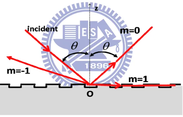
Theory of diffraction grating can be traced back to the beginning of 19th century
when T. Young and J. Fraunhofer made the first optical diffraction gratings and revealed the role of optical diffraction in their behavior. The scattering behaviors of diffraction gratings can be described basically by the conservation law of wave
momentum such as kscatt =kinc+G, where kscatt, kinc are the momentums of
scattered and incident wave momentum respectively, and G is the reciprocal lattice
reflecting grating showing an incident wave being scattered by the grating into three
orders, 0, m= m=1, and 1m= − . The idea of diffraction on grating didn’t be
challenged until Ebbesen’s findings [1]. Up to our best knowledge, before Ebbesen’s experiment, all studies had focused on the transmission of band-pass metal hole arrays occurring in the region, d< <
λ λ
c, where d is the lattice constant of the arrays,c
λ
is the cut-off wavelength for electromagnetic modes inside the holes, and λ isthe incoming wavelength. The long wavelength filtering is due to the cutoff by the holes, and the short wavelength filtering is due to occurring of energy redistribution when the first diffraction mode becomes propagating. However, Ebbesen found an
unexpected transmission spectra in the regime,
λ
c< <dλ
. Thus there must be adifferent mechanism responsible for this unexpected transmission spectra and promoted a study resurgence of such grating structures.
1.2 Wood’s Anomalies
“Wood’s anomalies” is observed by R. W. Wood, who discovered some unexpected patterns in the spectrum of light resolved by optical diffraction gratings, in 1902 [2]. Later than Wood’s discovery, Rayleigh and U. Fano explained the phenomenon respectively [3][4]. It is explained by Rayleigh that the energy of diffracted wave can be redistributed at specific diffracted orders. For instance, considering the case of Fig. 1.1, we note that the diffracted order, m=1 in the figure, becomes tangent to the grating surface just before its vanishing. In this case, the
normal momentum kz of diffracted wave becomes imaginary right after being zero.
Then the order (m=1) becomes evanescent in the direction of OZ axis. The energy
2 2
0 0// 0
k −k +G = and then be reflected. Therefore, there will be minima at the
transmission spectrum. We call it “Rayleigh’s anomaly”, and the wavelengths at which the minima occur are called “Rayleigh’s wavelengths”. Explanation to the peak of the spectrum is first proposed by U. Fano around 1938. He related the anomalies (peak) to a resonance effect. The resonances arise from the coupling between a discrete eigenmode of the grating and continuous diffraction modes. They occur right after the Rayleigh wavelengths. We call it “resonant anomalies”, or “Fano’s anomalies”.
Fig. 1.1 The schematic description of the process of diffraction. “m” is the diffraction
1.3 Surface Plasmon Polaritons
Surface plasmon is a surface wave due to collective oscillation of carriers (electrons) in conducting materials such as metals or doped semiconductors at optical
frequency[5]. This surface mode is confined at the interface between materials with
positive and negative dielectric constants respectively. Furthermore, if electromagnetic wave is coupled with the carriers at the surface, we call it surface plasmon polariton (SPP). To get a simple physical picture, we can consider the following situation: a stimulating electric field creates two opposite electric displacements in phase with each other across the interface. From Maxwell’s equations, we can see that these two opposite displacements act to attract and confine an AC current to the interface, and thus generate the collective oscillation of electrons. The mathematical description of the phenomenon of SPP can be referred to Ref. [5].
Then a dispersion relation of this non-radiative electromagnetic modecan be derived.
We don’t derive the dispersion relation here because in fact it is not the mechanism responsible for the phenomenon in our system.
1.4 Extraordinary Optical Transmission (EOT) through Sub-Wavelength
Metallic Hole Arrays
In 1998, Ebbesen et al. reported the surprising property of optical transmission on metallic gratings [1]. They drilled cylindrical holes (150nm for the diameter) in optically thick (200nm) metallic films in fashion of 2D lattice (900nm for the lattice constant) on a glass. Although bi-dimensional metallic gratings have been studied over many years before 1998, the most attractive characteristic of their findings was the distinct spectrum of transmission, as shown in the Fig. 1.2. In Fig. 1.2, the peculiar part of the spectrum is the transmission intensity at the wavelengths above
the periodicity, a0. We have already known that the minimum at a0 is the result of
Rayleigh type of Wood’s anomalies, and the peak right after a0 can, in general, be
explained by the Fano type. However, the peculiarity is that another peak occurs at even longer wavelength (1370nm) which is nearly ten times the hole diameter. Furthermore, if focusing on the transmission efficiency, one can find that the absolute transmission efficiency obtained by taking the ratio of total transmittance (zero-order) to the fraction of surface area occupied by the holes is larger than 2. That is, more than twice as much as energy can be transmitted through the holes when the light illuminates directly on hole area. This new phenomenon cannot be explained by Bethe’s theory which states that the transmission efficiency of a single sub-wavelength aperture can be described as ( / )r
λ
4 [6]. Apparently, the existence of grating does change the whole situation. Ebbesen attributed this phenomenon to the resonant excitation of surface plasmon polaritons (SPP). After Ebbesen, many researchers backed up this explanation by investigating this SPP-enhanced phenomenon both theoretically [7] [8] and experimentally [9]. However, there are other researchers questioning this SPP explanation. Theoretically they found that even a structure such as perfect electrical conductor (PEC) which cannot support surface plasmon on it also has a bounded surface wave on its surface [10][11], and hence can causes an extraordinary optical transmission [12]. Additionally, even both matter waves [13] and sound waves [14][15] through holey slabs show extraordinary transmission phenomenon.the skin depths of those metals can be calculated to be several tens of nanometers, and can be negligible when compared to the incident wavelength.
1.5 Spoof Surface Plasmon
In 2004, J. B. Pendry, et al. reported an original work showing that even a perfect conductor cam support confined surface wave as long as the surface are not purely flat [10]. The authors call this surface mode “Spoof Surface Plasmon”. Because such spoof surface plasmon (SSP) involves no carriers in the metal, they concluded that it is simply the geometry of the structure responsible for this surface mode. They also suggested that there will be a hybrid surface mode, which is the mixture of surface plasmon and spoof surface plasmon, on real metals. In their derivation, the long-wavelength approximation is assumed, i.e., the characteristic length of the structure are much smaller than the wavelength, and therefore the structured metal can be described as a homogeneous medium with effective dielectric constant and permeability. If a structure with characteristic length comparable to incoming wavelength is considered, the spoof surface plasmon still exists. In this case, the diffracted modes have also to be considered, and the main effect of the diffraction is to couple the confined spoof surface plasmon to free space. Therefore, an anomaly optical transmission can also occur when the incident light resonantly excites this surface mode. In the following part of the thesis, our theoretical ground will base on this result.
Chapter 2
Method of Measurement
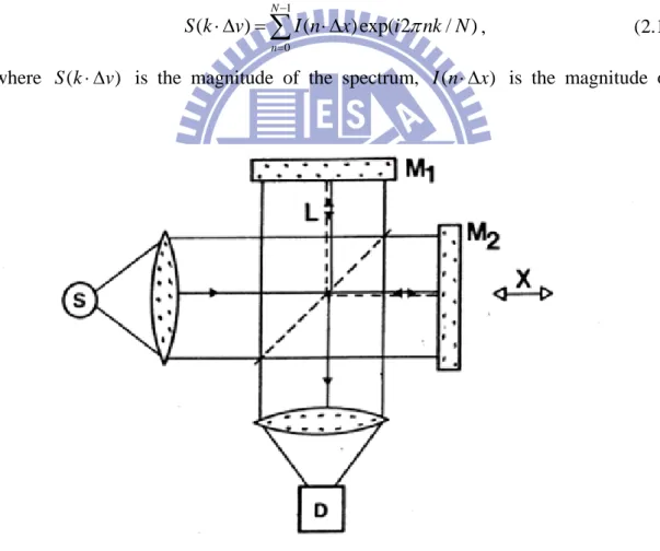
We used Fourier Transform Infrared Spectroscopy (FTIR) as our measurement method to analyze the transmission spectra of the devices under study in THz region. In this chapter, we will briefly introduce the fundamentals of FTIR method and the details of this measurement instrument. Fig. 2.1 is the basic schematics of a Michelson interferometer. A mercury lamp is used as the far-infrared light source. When light impinges on the beam splitter (50% transmitted and 50% reflected), the differences of light path can be adjusted by moving the mirrors, M1 and M2. In our instrument, M1 is held fixed while M2 is varied. As Fig. 2.1 shows, the reflected part of the light that goes to the fixed M1 in a distance L is reflected there and impinges on the beam splitter again after a total path of 2L. The same action happens to the transmitted part of the beam. Nevertheless, since the reflecting mirror M2 is not held fixed but can be moved very precisely back and forth around L by a distance x, the total path length of this light is consequently 2(L+x) . Then, when the two halves of the light recombine again on the beam splitter, they possess a path length difference of 2x and thus show a interference pattern. The light leaving the interferometer is then passed through the sample under test and is finally focused on the detector. In fact, the quantity measured by the detector is the intensity I(x) which is a function of moving mirror displacement x, the so-called interferogram. Here we use the zero crossings of the interferogram of He-Ne laser to sample that of the sample under measurement.
One of the advantages of FTIR is its measurement accuracy. The accuracy of the sampling spacing between two zero crossings is only determined by the precision of the laser wavelength itself. And the common FTIR spectrometers have a built-in
wavenumber calibration of high precision of about 0.01cm . Besides its high -1 accuracy, FTIR has others prior features to conventional IR grating spectrometers: the signal intensity. Because the circular apertures used in FTIR spectrometers have a larger area than the linear slit used in grating spectrometers, the throughput of light can be enhanced considerably. It is especially useful to the far-infrared measurement since the power density of general far-infrared light source is very weak. After data acquisition, we cannot directly read the spectrum information. The digitized, discrete and equidistant interferogram ( )I x must be converted to a spectrum S kv( ) by discrete Fourier transformation (DFT):
1 0 ( ) ( ) exp( 2 / ) N n S k v I n x i πnk N − = ⋅Δ =
∑
⋅Δ ,where (S k⋅ Δ is the magnitude of the spectrum, (v) I n⋅ Δ is the magnitude of x)
Fig. 2.1 Schematics of a Michelson interferometer. S: light source. D: detector. M1:
fixed mirror. M2: movable mirror. X: mirror displacement.
interferogram, Δx is the sampling distance, and Δv is the interval of the
frequency of the spectrum. The relation between Δv and Δx is as the following,
1 v
N x
Δ =
⋅Δ ,
where N is the number of sampling points.
The interferogram (I n⋅ Δ can be reconstructed by inverse discrete Fourier x)
transformation (IDFT): 1 0 1 2 ( ) ( ) exp( ) N n i nk I n x S k v N N π − = ⋅ Δ =
∑
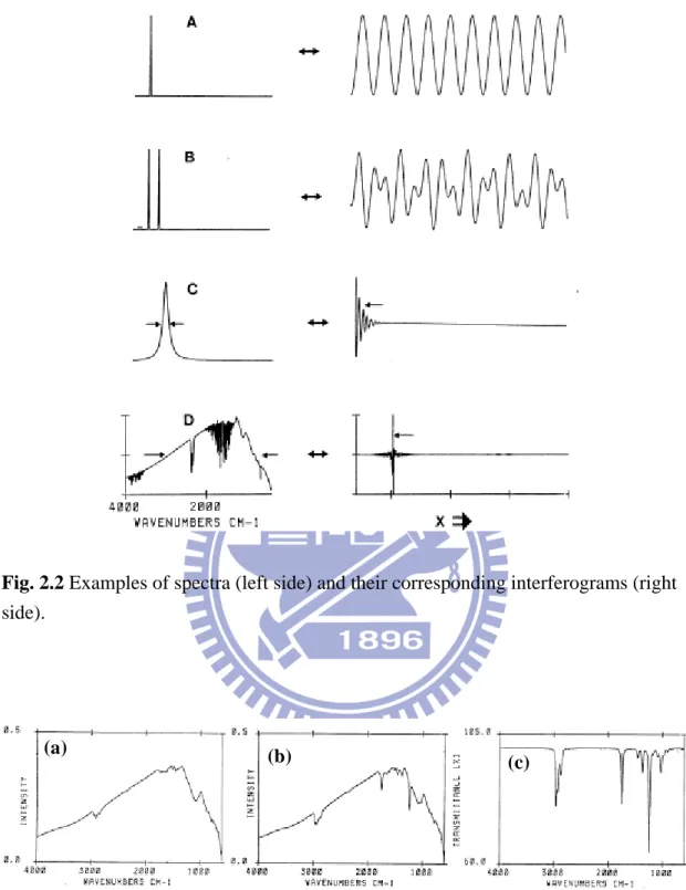
⋅ Δ − .The above is the mathematical fundamental of DFT. Fig. 2.2 shows some examples of Fourier Transform. The final transmittance spectrum can be obtained by three steps: a) an interferogram measured without sample in the optical path is Fourier transformed and generates the single channel reference spectrum R v (referred to Fig. 2.3(a)); b) ( ) an interferogram with a sample in the optical path is measured and Fourier
transformed and generate the single channel sample spectrum S v (referred to Fig. ( )
2.3(b)); c) the final transmittace spectrum T v is defined as ( ) ( ) ( )
( ) S v T v
R v
= (referred
to Fig. 2.3(c)). To further eliminate the H O2 and CO2 absorptions in THz region
of the optical path, we vacuum the chamber for every measurement. Some typical spectrums are shown in Fig. 2.3.
The type of FTIR instrument in our lab is “Bruker IFs66vs”, and the measurement
wavenumber range of liquid-He-cooled bolometer is from 50cm to 700-1 cm which -1
is equal to 14
μ
m to 200μ
m in wavelength.(2.2)
Fig. 2.2 Examples of spectra (left side) and their corresponding interferograms (right side).
Fig. 2.3 Three kinds of transmission spectra: (a) reference spectrum, (b) spectrum of
absorbing sample, (c) transmittance spectrum obtained by dividing (b) by (a).
(a) (b)
Chapter 3 Sample Design and Fabrication
Fig. 3.1 depicts the general profile of the samples fabricated by standard microlithography process. We defined the pattern by photolithography after coating the substrate surface with photoresist and then deposited 20nm-thick titanium for
adhesive layer on intrinsic 1cm 1cm× GaAs (
ε
GaAs =13.7 ) substrate and200nm-thick gold successively. Finally, a 2D hole array was perforated on the metal by lift-off process. The pattern on the metal was indeed a 2D Bravais lattice. It is known that there are five types of 2D Bravais lattices. Here we chose four types of lattices, which are square, rectangular, oblique, and triangular, to investigate the EOT phenomenon. To investigate the influence of hole shape on the transmission spectra, we varied the hole shape of the array with fixed periodicity. Especially we focused on square array with different hole shapes. As Fig. 3.2(a) shows, for square arrays, we
varied the hole widths from 18
μ
m to 3μ
m and with the hole lengths unchanged. InFig. 3.2(b) we did the same work but started the shrinking from 14
μ
m. It is shownthat both spectra in Fig. 3.2 have non-monotonous redshifts as the aspect ratios of holes are very large. On the other hand, we made the same pattern as Fig. 3.2(b) but with different metal, titanium, of 200nm thickness to see the influence of finite conductivity, as shown in Fig. 3.3. The finite conductivity effect can result in larger loss and enlarge the cutoff wavelength of the holes [26]. In Fig. 3.4, we kept the aspect ratio of the holes unchanged but shrank hole area gradually, and we found that the peak positions of the spectrum blueshift with decreasing full width at half maximum (FWHM). Moreover, we also studied the effect of symmetry difference between hole and lattice. It is known that any Bravais lattice has its unique primitive unit cell which is called Wigner-Seitz cell. A Wigner-Seitz cell has the full symmetry
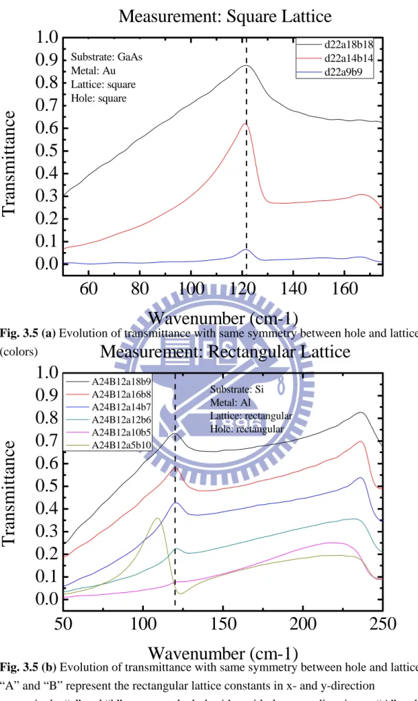
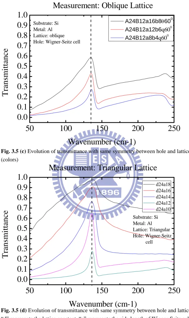
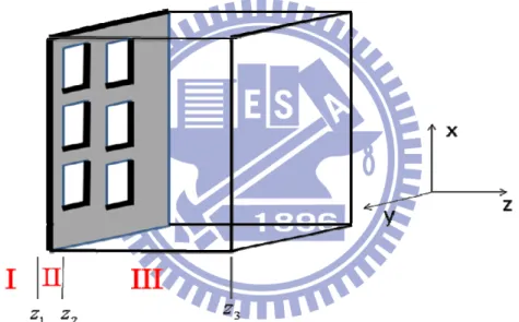
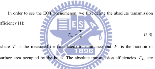
of the Bravais lattice, i.e., the Wigner-Seitz cell is as symmetrical as the Bravais lattice. Therefore, for each lattice, we defined the hole by Wigner-Seitz cell of the lattice. We found that if we kept the same symmetry but shrank the hole area, the peak position would be unchanged. The results are shown in Fig. 3.5(a)-(d). There is one thing that has to be mentioned: in Fig. 3.5(b), Fig. 3.5(c) and Fig. 3.5(d) the substrate material is changed to intrinsic silicon and the metal we use is 200nm-thick aluminum for economic consideration. The detailed discussion about these measurement results can be postponed until Chapter 5.
Fig. 3.1(a) Top-view of the sample under measurement. The gray region represents the substrate while the yellow region is the metal. (colors)
Fig. 3.2(a) Evolution of transmittance with various aspect ratios. d: lattice constant. a: the length of rectangular hole. b: the width of rectangular hole. (colors)
60
80
100
120
140
160
0.0
0.1
0.2
0.3
0.4
0.5
0.6
0.7
0.8
0.9
1.0
Substrate: GaAs Metal: Au Lattice: square Hole: rectangular 89.6umMeasurement
Trans
m
ittance
Wavenumber (cm-1)
d22a14b14 d22a14b12 d22a14b10 d22a14b8 d22a14b6 d22a14b5 d22a14b3 82.5um 83.5um 88.2um 86.5um 80.4um 85.8um60
80
100
120
140
160
0.0
0.1
0.2
0.3
0.4
0.5
0.6
0.7
0.8
0.9
1.0
Trans
m
ittance
Wavenumber (cm-1)
d22a18b18 d22a18b16 d22a18b14 d22a18b13 d22a18b12 d22a18b11 d22a18b10 d22a18b8 d22a18b5 d22a18b3 d22a18b2Measurement
82.5um 82.8um 94.5um 101.5um 102.3um 100.7um Substrate: GaAs Metal: Au Lattice: square Hole: rectangularFig. 3.3 Evolution of transmittance with low-conductive metal. d: lattice constant. a: the length of rectangular hole. b: the width of rectangular hole. (colors)
Fig. 3.4 Transmission spectra with fixed aspect ratio of the holes. d: lattice constant. a:
the length of rectangular hole. b: the width of rectangular hole. (colors)
60
80
100
120
140
160
0.0
0.1
0.2
0.3
0.4
0.5
0.6
0.7
0.8
0.9
1.0
Substrate: GaAs Metal: Au Lattice: square Hole: rectangularMeasurement
Trans
m
ittance
Wavenumber (cm-1)
d22a12b6 d22a14b7 d22a16b8 d22a18b9 97.7um 85.3um 88.4um 91.8um60
80
100
120
140
160
0.0
0.1
0.2
0.3
0.4
0.5
0.6
0.7
0.8
0.9
1.0
Substrate: GaAs Metal: Ti Lattice: square Hole: rectangularTrans
m
ittance
Wavenumber (cm-1)
Measurement
d22a14b14 d22a14b10 d22a14b8 d22a14b6 d22a14b3 83.2um 86.6um 90.4um 90.8um 91.4umFig. 3.5 (a) Evolution of transmittance with same symmetry between hole and lattice. (colors)
Fig. 3.5 (b) Evolution of transmittance with same symmetry between hole and lattice.
50
100
150
200
250
0.0
0.1
0.2
0.3
0.4
0.5
0.6
0.7
0.8
0.9
1.0
Substrate: Si Metal: Al Lattice: rectangular Hole: rectangularMeasurement: Rectangular Lattice
Tr
ansmittance
Wavenumber (cm-1)
A24B12a18b9 A24B12a16b8 A24B12a14b7 A24B12a12b6 A24B12a10b5 A24B12a5b1060
80
100
120
140
160
0.0
0.1
0.2
0.3
0.4
0.5
0.6
0.7
0.8
0.9
1.0
Substrate: GaAs Metal: Au Lattice: square Hole: squareMeasurement: Square Lattice
Transmittance
Wavenumber (cm-1)
d22a18b18 d22a14b14 d22a9b9
Fig. 3.5 (c) Evolution of transmittance with same symmetry between hole and lattice. (colors)
Fig. 3.5 (d) Evolution of transmittance with same symmetry between hole and lattice..
“d” represents the lattice constant. “a” represents the side length of Wigner-Seitz cell of triangular lattice. (colors)
50
100
150
200
250
0.0
0.1
0.2
0.3
0.4
0.5
0.6
0.7
0.8
0.9
1.0
Substrate: Si Metal: Al Lattice: oblique Hole: Wigner-Seitz cellMeasurement: Oblique Lattice
Trans
m
ittance
Wavenumber (cm-1)
A24B12a16b8θ600 A24B12a12b6q600 A24B12a8b4q60050
100
150
200
250
0.0
0.1
0.2
0.3
0.4
0.5
0.6
0.7
0.8
0.9
1.0
Substrate: Si Metal: Al Lattice: Triangular Hole: Wigner-Seitz cellMeasurement: Triangular Lattice
Wavenumber (cm-1)
Tr
ansmittance
d24a18 d24a16 d24a14 d24a12 d24a10Chapter 4 Theoretical Formalism
In order to analyze the experimental data and understand the physics involved in the 2D structure, we have to do the calculation based on modal expansion. The unit system we adapt here is SI units.
First of all, we divide the whole system into three regions which are I, II, and III
respectively as shown in Fig. 4.1(b). RegionI is the region of reflection where the
EM fields can be expanded by the eigenmodes of Helmholtz’s equations in free space and the incident light is given in this region. RegionII is the structure region where the EM fields inside the hole can be expanded by rectangular waveguide modes of
perfect electrical conductor (PEC). RegionIII is the substrate region which can be
seen as another kind of free space except the light velocity there has to be divided by refraction index of the substrate material. The 2D structure under study is an infinite array of holes drilled periodically in a metal film of thicknessh. Fig. 4.1(a) depicts
the definition of the primitive unit cell. The primitive unit cell is defined as a rectangular with length and width being A, B respectively, while the length and width of the rectangular hole inside the unit cell is denoted by a, b respectively.
We start from the Maxwell’s equations for complex time-harmonic fields in source free case:
0 ( ) i
ωμ
( ) 0 ∇×H r − E r = 0 ( ) iωε ε
( ) ( ) 0 ∇×E r + r H r = (4.1) (4.2)0 ( ) ( ) 0
ε ε
∇⋅ r E r = ,
where the related coefficients are the same as the standard notations in any electromagnetic textbook. In the following derivation, the only approximation we make is that the metal is considered to be perfect electrical conductor (PEC). This is a good approximation because our system is operated in THz region, where the skin depth of the metal with good conductivity is about only several tens of nanometer. Combine (4.1) and (4.2) , we obtain
2 0 1 ( ) c ω ε ε ⎛ ⎞ ⎛ ⎞ ∇ ×⎜ ∇ × ⎟ ⎜ ⎟= ⎝ ⎠ ⎝ r H⎠ H
(
)
0 ( ) 2 c ω ε ε ⎛ ⎞ ∇× ∇× = ⎜ ⎟ ⎝ ⎠ E r E .After further manipulation we can obtain two Helmholtz’s equations,
2 2 0 ( ) ( ) ( ) 0 c ω ε ε ⎛ ⎞ ∇ + ⎜ ⎟ = ⎝ ⎠ E r r E r and 2 2 0 ( ) ( ) 0 c ω μ ⎛ ⎞ ∇ + ⎜ ⎟ = ⎝ ⎠ H r H r .
Both electric and magnetic fields satisfy the above two Helmholtz’s equations in each region. At any boundary the EM fields in between the regions satisfy the following boundary conditions,
(
μ1 1 μ2 2)
0 ⋅ − = n H H(
1 2)
s × − = n H H J(
ε1 1 ε2 2)
ρs ⋅ − = n E E(
1 2)
0 × − = n E E , (4.4) (4.5) (4.6) (4.7) (4.8) (4.9) (4.10) (4.11) (4.12)where the numbers of subscripts mean different regions, n is the unitary vector
normal to the surface, and Js and
ρ
s are surface current and surface chargerespectively. In the following, we will first attack this problem at each region individually and then match the boundary conditions at the interface of each region. All EM fields at each region are governed by (4.7) and (4.8) . To simplify the derivation, we learned from Garcia’s paper in 2008 [16] to use Dirac’s notation for representation of each field, or eigenfunction. For example, the electric field can be
written as E r( )= r E// E z( ) . The reason why we deliberately separate the
z-dependent function from Dirac’s notation will be apparent in our derivation soon. To further simplify the derivation, according to Garcia, for the same mode E-field and H-field have the following relation
mode Ymode mode
− ×z H = ± E ,
where Ymode is the modal admittance. The choice of + or – depends on the
propagation direction +z or –z respectively. Consequently we can consider only the eigenmodes of electric field.
Basically, we can categorize the system into two types, the free space type and the inside hole type. In free space, the eigenmodes of (4.7) are plane waves obeying Bragg diffraction law, i.e., k=k0+G, where k0 and k are incident and reflected
wavevectors respectively, and 2 (m n )
A B
π
= +
G x y . In the previous expression ( , )m n
denoting the diffraction order is a pair of arbitrary integers. Moreover, the plane wave eigenmodes can be further decomposed to two orthogonal functions based on the directions of polarization, p and s. The definitions of p- and s-polarizations are shown
Fig. 4.1(a) Top view of unit cell of the rectangular lattice.
Fig. 4.1(b) Schematics of the system under study.
which can be denoted by TE,pq and TM,pq , where ( , )p q represents a certain order of waveguide mode.
After choosing the expansion basis with consideration of Bloch’s theorem, we can write down the EM fields in different regions:
z Region I, (z<0)
Given a normal incident wave, the EM fields can be expressed as follows,
{
}
(1) 1 ,00 (1) (1) , 1 , 1 ( ) I (1) (1) inc, inc, ( ) ( ) (1) (1) ( ) 00 00 z z mn z mn ik z z p s ik z z ik z z mnp mns mn z a p a s e b mnp e b mns e − − − − − = + + ⎡ + ⎤ ⎣ ⎦∑
E{
}
(1) 1 ,00 (1) (1) , 1 , 1 ( ) I (1) (1) (1) (1) inc, 00 inc, 00 ( ) ( ) (1) (1) (1) (1) ( ) 00 00 z z mn z mn ik z z p p s s ik z z ik z z mnp mnp mns mns mn z a Y p a Y s e b mnp Y e b Y mns e − − − − − − × = + − ⎡ + ⎤ ⎣ ⎦∑
z H , where 2 2 2 (1) , 2 2 z mn m n k c A B ω π π ⎛ ⎞ ⎛ ⎞ ⎛ ⎞ = ⎜ ⎟ −⎜ ⎟ −⎜ ⎟ ⎝ ⎠ ⎝ ⎠ ⎝ ⎠ (1) 0 (1) , mnp z mn Y k ωε = (1) , (1) 0 z mn mns k Y ωμ =and bmnp(1) , bmns(1) are coefficients to be calculated.
z Region II, (z1< <z z2)
(
)
(
)
( 2 ) ( 2 ) , 1 , 2 0 ( 2 ) ( 2 ) , 1 , 2 ( ) ( ) (2) (2) TM, TM, II ( ) ( ) (2) (2) TE, TE, TM, , ( ) TE, , z pq z pq z pq z pq ik z z ik z z pq pq pq i ik z z ik z z pq pq pq a e b e z e pq a e b e − − − ⋅ − − − ⎡ + +⎤ ⎢ ⎥ ⎢ ⎥ = ⎢ + ⎥ ⎢ ⎥ ⎣ ⎦∑
∑
∑
k R R R E R (4.14) (4.15) (4.16) (4.17) (4.18) (4.19)(
)
(
)
( 2 ) ( 2 ) , 1 , 2 0 ( 2 ) ( 2 ) , 1 , 2 ( ) ( ) (2) (2) (2) TM, TM, TM, II ( ) ( ) (2) (2) (2)TE, TE, TE,
TM, , ( ) TE, , z pq z pq z pq z pq ik z z ik z z pq pq pq pq i ik z z ik z z pq pq pq pq Y pq a e b e z e Y pq a e b e − − − ⋅ − − − ⎡ − +⎤ ⎢ ⎥ ⎢ ⎥ − × = ⎢ − ⎥ ⎢ ⎥ ⎣ ⎦
∑
∑
∑
k R R R z H R , where 2 2 2 ( 2) , z pq p q k c a b ω π π ⎛ ⎞ ⎛ ⎞ ⎛ ⎞ = ⎜ ⎟ −⎜ ⎟ −⎜ ⎟ ⎝ ⎠ ⎝ ⎠ ⎝ ⎠ (2) 0 TM, (2) , pq z pq Y k ωε = (2) , (2) TE, 0 z pq pq k Y ωμ =R is the position vector on the x-y plane and aTM,pq(2) , ( 2) TE,pq a , bTM,pq( 2) , (2) TE,pq b are coefficients to be calculated. z Region III, (z>z2) ( 3) ( 3) , ( 2) , ( 2) III (3) (3) ( ) ikz mn z z ikz mn z z mnp mns mn z =
∑
⎡⎣a mnp e − +a mns e − ⎤⎦ E ( 3) ( 3) , ( 2) , ( 2) III (3) (3) (3) (3) ( ) ikz mn z z ikz mn z z mnp mnp mns mns mn z ⎡a mnp Y e − a Y mns e − ⎤ − ×z H =∑
⎣ + ⎦, where 2 2 2 (3) , 2 2 z mn GaAs m n k c A B ω ε π π ⎛ ⎞ ⎛ ⎞ ⎛ ⎞ = ⎜ ⎟ −⎜ ⎟ −⎜ ⎟ ⎝ ⎠ ⎝ ⎠ ⎝ ⎠ (3) 0 (3) , GaAs mnp z mn Y k ωε ε = (3) , (3) 0 z mn mns k Y ωμ = and amnp(3) , (3) mnsa are coefficients to be calculated.
Now we write down the real space expression for each eigenmode explicitly:
(4.20) (4.28) (4.27) (4.26) (4.25) (4.21) (4.22) (4.23) (4.24)
2 2 ( ) // 2 2 2 1 2 2 2 m n i x y A B m A mnp e n m n AB B A B π π π π π π + ⎡ ⎤ ⎢ ⎥ = ⎢ ⎥ ⎡⎛ ⎞ ⎛ ⎞ ⎤ ⎢ ⎥ + ⎢⎜⎝ ⎟⎠ ⎜⎝ ⎟ ⎣⎠ ⎥ ⎢ ⎥⎦ ⎢ ⎥ ⎣ ⎦ r , if m n, are nonzero. 2 2 ( ) // 2 2 2 1 2 2 2 m n i x y A B n B mns e m m n AB A A B π π π π π π + − ⎡ ⎤ ⎢ ⎥ = ⎢ ⎥ ⎡⎛ ⎞ ⎛ ⎞ ⎤ ⎢ ⎥ + ⎢⎜⎝ ⎟⎠ ⎜⎝ ⎟ ⎣⎠ ⎥ ⎢ ⎥⎦ ⎢ ⎥ ⎣ ⎦ r , if m n, are nonzero. // 1 1 00 0 p AB ⎡ ⎤ ≡ ⎢ ⎥ ⎣ ⎦ r // 0 1 00 1 s AB ⎡ ⎤ ≡ ⎢ ⎥ ⎣ ⎦ r
(
)
(
)
(
)
(
)
// 2 2 2 cos sin 1 TM, , 2 sin cos x y x y p p q x R y R a a b pq q p q p q x R y R ab b a b a b π π π π π π π π ⎡ ⎛ − ⎞ ⎛ − ⎞⎤ ⎜ ⎟ ⎜ ⎟ ⎢ ⎝ ⎠ ⎝ ⎠⎥ ⎢ ⎥ = ⎢ ⎛ ⎞ ⎛ ⎞⎥ ⎡⎛ ⎞ ⎛ ⎞ ⎤ − − ⎢ ⎜ ⎟ ⎜ ⎟⎥ + ⎢⎜ ⎟ ⎜ ⎟ ⎥ ⎣ ⎝ ⎠ ⎝ ⎠⎦ ⎝ ⎠ ⎝ ⎠ ⎢ ⎥ ⎣ ⎦ r R , if p q, are nonzero.(
)
(
)
(
)
(
)
// 2 2 2 cos sin 1 TE, , 2 sin cos x y x y q p q x R y R b a b pq p p q p q x R y R ab a a b a b π π π π π π π π ⎡− ⎛ − ⎞ ⎛ − ⎞⎤ ⎜ ⎟ ⎜ ⎟ ⎢ ⎝ ⎠ ⎝ ⎠⎥ ⎢ ⎥ = ⎢ ⎛ ⎞ ⎛ ⎞⎥ ⎡⎛ ⎞ ⎛ ⎞ ⎤ − − ⎢ ⎜ ⎟ ⎜ ⎟⎥ + ⎢⎜⎝ ⎟⎠ ⎜⎝ ⎟⎠ ⎥ ⎣ ⎝ ⎠ ⎝ ⎠⎦ ⎢ ⎥ ⎣ ⎦ r R , if p q, are nonzero.There is one important thing that has to be mentioned. For TE waveguide modes,
// TE,pq
r , if p=0 or q= , the normalization must be amended by multiplication 0
(4.33) (4.34) (4.32) (4.31) (4.30) (4.29)
surface have to be continuous everywhere on the surface and magnetic fields parallel to the surface have to be continuous on the holes area. Therefore, as Garcia did, we project the matching equations onto plane wave eigenmodes for electric fields and rectangular waveguide eigenmodes for magnetic fields. Besides, we can match the
boundary only on one Wigner-Seitz unit cell, i.e., R=0, because our structure has
perfect periodicity and thus satisfies Bloch’s theorem. Therefore we can abbreviate
TM,pq,R=0 and TE,pq,R=0 to TM,pq and TE,pq respectively. The
boundary conditions are matched at two interfaces:
At z=z1 (z1− = −z2 h): For E-field, I II 1 1 (z=z) = (z=z) E E .
Then multiply (4.35) by mnp and mns separately and do integration over an
area of unit cell to obtain
{
}
(
( 2 ))
(
( 2 ))
, , (1) (1) (1) inc, 0 0 inc, 0 0 (2) (2) (2) (2) TM, TM, TE, TE, TM, z pq TE, z pq p m n p s m n sp mn ik h ik h pq pq pq pq pq pq a a b mn pq a b e mn pq a b e σ σ δ δ δ δ δ δ σ σ + + = + + +∑
∑
, where , p sσ
= 1, if 0, if mn m n m nδ
= ⎨⎧ = ≠ ⎩ . For H-field, I II 1 1 (z z ) (z z ) − ×z H = = − ×z H =Then multiply (4.39) by TM,pq and TE,pq separately and do integration over
(4.39) (4.38) (4.37)
(4.36) (4.35)
an area of a hole to obtain
{
}
(
( 2 ))
, (1) (1) (1) (1) inc, 00 inc, 00 (1) (1) (1) (1) (2) (2) (2) , , , 00 00 z pq p p s s ik h mnp mnp mns mns pq pq pq mn a Y p a Y s b Y mnp b Y mns Yα aα bα e α α α α + − ⎡ + ⎤= − ⎣ ⎦∑
, where TM, TE α = . At z=z2 (z2− =z1 h): For E-field, III II 2 2 (z=z ) = (z=z ) E EThen multiply (4.42) by mnp and mns separately and integrate over the area
of unit cell to obtain
(
)
(
)
( 2) , ( 2 ) , (1) (2) (2) TM, TM, (2) (2) TE, TE, TM, TE, z pq z pq ik h mn pq pq pq ik h pq pq pq a mn pq a e b mn pq a e b σ σ σ = + + +∑
∑
, where , p sσ
= . For H-field, III II 2 2 (z z ) (z z ) − ×z H = = − ×z H = (3.45)(
( 2 ))
, (3) (3) (3) (3) (2) (2) (2) , , , z pq ik h mnp mnp mns mns pq pq pq mn a Y α mnp a Y α mns Yα aα e bα ⎡ + ⎤= − ⎣ ⎦∑
where TM, TE α = .With the four simultaneous equations (4.36), (4.40), (4.43), and (4.46) , we can (4.47) (4.46) (4.44) (4.43) (4.42) (4.41) (4.40)
[ ]
TM, TE, TM, TE, mnp pq mnp pq mns pq mns pq ⎡ ⎤ ⎢ ⎥ ⎢ ⎥ = ⎢ ⎥ ⎢ ⎥ ⎣ ⎦ M L L M O M O L L M O M O[ ]
( 2 ) , ( 2 ) , 0 0 0 0 0 0 0 0 z pq z pq ik h ik h e e ⎡ ⎤ ⎢ ⎥ ⎢ ⎥ = ⎢ ⎥ ⎢ ⎥ ⎢ ⎥ ⎣ ⎦ E L O M M L O[ ]
(1) 1 (1) 0 0 0 0 0 0 0 0 mnp mns Y Y ⎡ ⎤ ⎢ ⎥ ⎢ ⎥ = ⎢ ⎥ ⎢ ⎥ ⎣ ⎦ Y L O M M L O[ ]
(2) TM, 2 (2) TE, 0 0 0 0 0 0 0 0 pq pq Y Y ⎡ ⎤ ⎢ ⎥ ⎢ ⎥ = ⎢ ⎥ ⎢ ⎥ ⎣ ⎦ Y L O M M L O[ ]
(3) 3 (3) 0 0 0 0 0 0 0 0 mnp mns Y Y ⎡ ⎤ ⎢ ⎥ ⎢ ⎥ = ⎢ ⎥ ⎢ ⎥ ⎣ ⎦ Y L O M M L O[ ]
(1) (1) T 1 = ⎣⎡0 0 ainc,p 0 ainc,s 0 0⎤⎦ a L L[ ]
(1) (1) T 1 = ⎣⎡bmnp bmns ⎤⎦ b L L[ ]
(2) (2) T 2 = ⎣⎡aTM,pq aTE,pq ⎤⎦ a L L[ ]
(2) (2) T 2 = ⎣⎡bTM,pq bTE,pq ⎤⎦ b L L[ ]
(3) (3) T 3 = ⎣⎡amnp amns ⎤⎦ a L L[ ]
(3) (3) T 3 = ⎣⎡bmnp bmns ⎤⎦ b L L .Thus (4.36), (4.40), (4.43), and (4.46) can be expressed as
(4.58) (4.57) (4.56) (4.55) (4.54) (4.53) (4.52) (4.51) (4.50) (4.49) (4.48)
[ ] [ ] [ ][ ] [ ][ ][ ]
a1 + b1 = M a2 + M E b2[ ] [ ] [ ] [ ]
†{
}
[ ] [ ] [ ][ ]
{
}
1 1 − 1 = 2 2 − 2 M Y a b Y a E b[ ] [ ] [ ][ ] [ ]
a3 = M{
E a2 + b2}
[ ] [ ][ ] [ ] [ ][ ] [ ]
†{
}
3 3 = 2 2 − 2 M Y a Y E a b .With (4.53) being given and the four matrix equations (4.59), (4.60), (4.61) and (4.62) , we can determine the four column matrices (4.54), (4.56), (4.57) and (4.58) . The last step is to calculate the transmittance of this system. Because the system is considered to be lossless, the transmittance in each region must be equal. We use Poynting’s theorem to calculate the energy flux through a unit cell at a given z,
( )
(
)
*(
)
unit cell 1 ˆ Re , , , , d d 2 J z = ⎧⎨ ⋅⎡⎣ x y z × x y z ⎤⎦ x y⎫⎬ ⎩∫∫
z E H ⎭ v v .Finally, the transmittance can be obtained by dividing ( )J z by incoming energy flux
0 J . (4.63) (4.62) (4.61) (4.60) (4.59)
Chapter 5 Simulation Results and Discussions
5.1 Preamble
In Chapter 4, our formalism is based on rectangular (or square) Bravais lattice and rectangular (or square) lattice basis (hole) for simplicity. Therefore, in this chapter, we will compare our simulation results with measurement ones restricted only to rectangular (or square) case. The dielectric constants of the substrate will be chosen to be either
ε
Si =11.9 orε
GaAs =13.7, just for matching the measurement conditions. The real dielectric constants of substrate imply that the substrate is assumed to be lossless material. The incident light in our simulation is set to be 45 -polarized for 0 including the two possible polarizations. Besides, let us recall the two assumptions of calculation presented in Chapter 4. The first assumption is that the metal is a perfect electric conductor, so there is no EM field penetrating into the metal and apparently no surface plasmon polariton effect is considered. This is a good assumption because in our case the light frequency is at THz regime and the skin depth of the field into the metal with good conductivity can be calculated as the following [17],1
2
δ
μσ ω
= ,
where
μ
is the magnetic permeability of the metal, ω is the angular frequency,and
σ
1 is the real part of conductivity which can be related to imaginary part of dielectric constantε
2 by [18]( )
2 1 2 4 ωε σ π = .Since
ε
2 of gold is a very large value (larger than 80000) in THz regime [19], the(5.1)
skin depth can be calculated to be approximately 35nm which is around 1/10000 of the incident wavelength. The second assumption is that the substrate thickness is assumed to be infinite, i.e., we don’t consider the dielectric waveguide effect and interference of three layer system caused by the substrate. This also can be neglected
because the accuracy Δk in our measurement is set to be large enough (say, 4cm ) -1
to make the interference due to substrate thickness unresolved in the spectrum. As to dielectric waveguide effect, our definition of transmittance1 can minimize this effect.
5.2 Simulation Results Compared with Measurement Results:
EOT Phenomenon
Fig. 5.1 shows the (zero-order) transmittance spectra of both simulation and
experiment results. We can see that the simulation gives a very good agreement with the measured spectrum position of peak transmittance. However, there still is discrepancy between simulation and measurement results in the magnitude of peak transmittance and linewidth, or FWHM. The reason should be that we didn’t consider the loss of metal in our calculation and in practice the 2D hole array can never be ideally periodic.
In order to see the EOT phenomenon, we first define the absolute transmission efficiency [1]: abs T T F = ,
where T is the measured (or calculated) transmittance and F is the fraction of
surface area occupied by the holes. The absolute transmission efficiencies Tabs are
1.4 and 1.3 for simulation and measurement results in Fig. 5.1 respectively. Tabs’ s
being larger than 1 means that the transmitted light is more than that impinges on the holes directly. This is exactly the so-called EOT phenomenon. The peak positions occur near the lattice periodicity with consideration of substrate refraction index. Therefore we know that it is mainly the lattice periodicity of the structure that makes such EOT phenomenon. Again we have to emphasize that it is a purely geometric effect because our metal is seen as PEC. No surface plasmon polariton is considered. The absolute transmission efficiency becomes larger when we reduce the hole area, as shown in Fig. 5.2. In Fig. 5.2, we reduce the hole widths from 14um to 0.5um gradually of the 2D structure with lattice constant, d=22um, and fixed hole length, (5.3)
a=14um, on a substrate of dielectric constant,
ε
GaAs =13.7 . The transmission efficiency will be very large if we let the hole area be very small. This high efficiency implies that the strength of EM field is very large inside the holes. Or we can say that the energy of light impinging on the metal surface with 2D hole array is “squeezed” into the holes. In fact, this phenomenon is similar to resonant tunneling in quantum mechanics. In the case of resonant tunneling, as shown in Fig. 5.3, if L1 is equal to L2, namely, the system is symmetric in the direction of transmission, there will be a 100% transmission regardless of the barrier heights and barrier widths, as shown in Fig. 5.8. Corresponding to our 2D metal hole array case which is assumed to be symmetric in the direction of transmission (i.e., free standing film), then no matter how small the holes area is, if the incoming wave can exactly couple to an isolated state of the system, the transmission of the wave can reach 100%, as shown in Fig. 5.4. If the system in the transmission direction is not symmetric (i.e., metal on a GaAs substrate), the transmittance will not reach 100% anymore, but still can have a very high transmission efficiency. We can see from Fig. 5.7 for instance. We can also see this non-100% transmission for resonant tunneling in quantum mechanics, as shown inFig. 5.5. Thus in principle it is convenient to make an analogy to resonant tunneling in
quantum mechanics for our EOT phenomenon. With extremely large field inside the holes, an interesting application arises. That is, we can fill some optically linear materials into the holes. Those materials inside the holes will experience a remarkably large EM field, leading to non-linear optical response.
Fig. 5.1 The comparison between measured and calculated transmittance spectrum.
(colors)
Fig. 5.2 The absolute transmission efficiencies with various holes. In this case we fix
one side of the hole and vary the other side gradually.
60
80
100
120
140
160
0.0
0.1
0.2
0.3
0.4
0.5
0.6
0.7
0.8
0.9
1.0
Substrate: GaAs Metal: Au Lattice: square Hole: squareTransmittance
Wavenumber (cm-1)
d22a18b18 (measured) d22a18b18 (calculated)16
14
12
10
8
6
4
2
0
0
5
10
15
20
25
30
35
d22a14 (calculated) d22a14 (measured)Absolute Transmis
sion Ef
ficiency
Fig. 5.3 L1 and L2 are the widths of the two barriers respectively. W is the width of
the well..V is the barrier height.
Fig. 5.4 Transmittance spectrum for free standing (the upper and lower dielectric
100
200
300
400
500
600
0.0
0.2
0.4
0.6
0.8
1.0
Simulation
Tr
ansm
ittance
Wavenumber (cm-1)
d22a14b14h0.2 (free standing)Fig. 5.5 Transmission spectrum of resonant tunneling in quantum mechanics with
5.3 Simulation Results Compared with Measurement Results:
Non-Monotonous Red-Shift Phenomenon
In Fig. 3.2, we see that the spectrum positions of peak transmittance are mostly red-shifted with increase of the aspect ratio of the holes. This red-shifted evolution has been shown and partially explained in the previous literatures [20][21][22]. While the authors in Ref. [22] attributed the red-shifted effect to the coupling between a discrete resonant state and continuum non-resonant states which is based on Fano-type resonance [23], others in Ref. [20][21] attributed the shifts to the localized resonance (or shape resonance). However, in our experiment, we found that the shift evolution is not monotonous as a function of the aspect ratio of the holes. When we continue to shrink the hole widths, i.e., to increase the aspect ratio of the holes, the peak positions eventually shift to blue. Our simulations also confirm this non-monotonous phenomenon, as shown in Fig. 5.6(a)-(d). In Fig. 5.6(a)-(d) we can also note that there are minima occurring soon after the peaks. It is the so-called “Wood’s anomaly” of Rayleigh’s type (referred to Chapter 1). This is because that the incoming light satisfies the relation, k02−k0 //+G2 =0 and then becomes grazing
to the surface, where k0 is the incident wavevector in free space, k0 // is the
in-plane component of the incident wavevector, and G is the reciprocal lattice
vector. Thus the spectrum positions of the minima only depend on the lattice periodicity, as can be seen in Fig. 5.6(b). In 2005, F. J. Garcia, et al. derived that even a “single” hole perforated on PEC film can show a resonance near the cut-off wavelength of the hole [24]. Moreover, they made a conclusion that a rectangular hole
phenomenon. This result confirmed that there is surely a localized resonance at individual hole. In fact, the hole can be seen as an open-ended metallic low-quality-factor (low-Q) resonator [25]. This localized resonance is leakier than the discrete resonant mode caused by lattice periodicity, and it will affect the spectrum position of peak transmittance and the linewidth. In order to obtain a more physical picture, we consider this phenomenon in a simpler way. First of all, the EOT phenomenon in our case (normal incidence) is not because of a surface EM wave resonance but because of the constructive interference of evanescent wave. The reason is that our incident light is normal to the surface of the 2D structure (k0, // =0),
corresponding to the Γ point of the band structure of the system. The band structure
of PEC film with 2D hole array perforated on it has been calculated by Z. Ruan and M.
Qiu [25]. From the band structure in Ref. [25] we see that there are modes at the Γ
point and the frequencies of those modes are very close to the spectrum position of transmission peak at normal incidence. However, what they considered is the free standing metallic film with symmetry in the z-direction while in our case the system is asymmetric (with substrate) in the z- direction. Thus it is no necessary to take into account the odd and even modes. The role of each hole can be seen as the source of evanescent field in the z-direction. Then each evanescent field forms constructive interference through the 2D periodicity. Basically the periodicity (lattice constant) determines the spectrum position of transmission peak. The hole shapes (lattice basis) will modify the band structure of the system. An apparent influence on the transmission spectrum by the holes is the linewidth. The larger the hole area, the more broadening the spectrum. This can be seen in Fig. 5.7. An analogy of two-barrier-one-well band structure in quantum mechanics can illustrate this idea. The transmission characteristics of such structure with different barriers are shown in Fig.
5.8. This is the well-known resonant tunneling in quantum mechanics. We can see that
the resonant mode is leakier (wider linewidth, as in Fig. 5.8(a)) with narrower potential barrier. In our structure, the larger hole corresponds to narrower potential barrier while the smaller hole corresponds to wider potential barrier.
To be more detailed, we still have to distinguish the total mechanism into hole resonance and periodicity resonance. We take Fig. 5.6 for illustrating example. Before that, in particular, one point has to be mentioned: the polarization preference. In our simulation, we found that as the hole width b (referred to Fig. 4.1) decreases, the transmittance will prefer the y-axis-polarized electric field of the incident light. This result is common to Ref. [21]. Therefore, as the hole width is kept shrinking, the structure shall allow only one direction (y-axis) of the polarization of incoming light eventually. This polarization-selective characteristic can be shown in Fig. 5.9.
Therefore, the cut-off wavelength
λ
cut-off of a rectangular PEC waveguide isdetermined by its long length, a (referred to Fig. 4.1). In our example (Fig. 5.6(c)),
cut-off 28 m
λ
=μ
, which is larger than the lattice constant, d=22 mμ . Based on Ref.[24], it is shown that the more the aspect ratio of the hole, the stronger the localized resonance (higher quality factor). Therefore, the spectrum positions of the peak transmittance will redshift with the increasing aspect ratio. Nevertheless, if the cut-off wavelength of the hole is equal to or smaller than the lattice periodicity, the peak can hardly shift, as shown in Fig. 5.10. Now let’s go back to Fig. 5.6. As we continue to shrink the hole widths, the peak positions eventually shift back. In general, we know that the higher the quality factor, the lower the coupling strength. So we
Fig. 5.6(a) Evolution of transmittance spectra with various aspect ratios. (colors)
Fig. 5.6(b) Evolution of transmittance spectra with various aspect ratios. (colors)
60
80
100
120
140
160
0.0
0.1
0.2
0.3
0.4
0.5
0.6
0.7
0.8
0.9
1.0
Substrate: ε=13.7 Metal: PEC Lattice: square Hole: rectangularSimulation
Transmittance
Wavenumber (cm-1)
d22a18b18 d22a18b16 d22a18b14 d22a18b13 d22a18b12 d22a18b11 d22a18b10 d22a18b8 d22a18b5 d22a18b3 d22a18b2 d22a18b0.560
80
100
120
140
160
0.0
0.1
0.2
0.3
0.4
0.5
0.6
0.7
0.8
0.9
1.0
Substrate: GaAs Metal: Au Lattice: square Hole: rectangularTrans
m
ittance
Wavenumber (cm-1)
d22a18b18 d22a18b16 d22a18b14 d22a18b13 d22a18b12 d22a18b11 d22a18b10 d22a18b8 d22a18b5 d22a18b3 d22a18b2Measurement
82.5um 82.8um 94.5um 101.5um 102.3um 100.7umFig. 5.6(c) Evolution of transmittance spectra with various aspect ratios. (colors)
60
80
100
120
140
160
0.0
0.1
0.2
0.3
0.4
0.5
0.6
0.7
0.8
0.9
1.0
Substrate: 13.7 Metal: PEC Lattice: square Hole: rectangularSimulation
Transmittance
d22a14b14 d22a14b12 d22a14b10 d22a14b8 d22a14b6 d22a14b5 d22a14b3 d22a14b1 d22a14b0.560
80
100
120
140
160
0.0
0.1
0.2
0.3
0.4
0.5
0.6
0.7
0.8
0.9
1.0
Substrate: GaAs Metal: Au Lattice: square Hole: rectangular 89.6umMeasurement
Tr
ansmittance
Wavenumber (cm-1)
d22a14b14 d22a14b12 d22a14b10 d22a14b8 d22a14b6 d22a14b5 d22a14b3 82.5um 83.5um 88.2um 86.5um 80.4um 85.8umTM,pq )2. When the coupling strength decreases to a certain degree, the influence of the hole resonance becomes minor and periodicity resonance dominates. In fact, it is hard to separate the hole resonance and periodicity resonance in this system because they are coupled together. However, we can obtain some clues when we change the lattice constant but fix the hole size and shape. As can be seen in Fig. 5.11, the minima of the spectra change exactly with the lattice constant while the peaks change more slowly. Notice that the labeled wavelengths have to be divided by refraction index of the substrate. Also, we can see that when the difference in dimension between the lattice constant and hole gets larger, the peaks is more indifferent to the changes of lattice constant. This signals the weaker coupling between hole and periodicity resonance.
2
Fig. 5.7 Evolution of transmittance spectra. (colors)
60
80
100
120
140
160
0.0
0.1
0.2
0.3
0.4
0.5
0.6
0.7
0.8
0.9
1.0
Substrate: ε=13.7 Metal: PEC Lattice: squareHole: Wigner-Seitz cell
Simulation
Trans
m
ittance
Wavenumber (cm-1)
d22a18b18 d22a14b14 d22a12b12 d22a11b11 d22a10b10 d22a9b9Fig. 5.8 (a) The transmission of resonant tunneling with narrower barriers [27].
Fig. 5.9 Polarization dependence.
60
80
100
120
140
160
0.0
0.2
0.4
0.6
0.8
1.0
100 200 300 400 500 600 700 0.000 0.002 0.004 0.006 0.008 0.010 0.012 0.014 Substrate: ε GaAs=13.7 Metal: PEC Lattice: square Hole: rectangular x-axis polarizationSimulation
Trans
m
ittance
Wavenumber (cm-1)
d22a14b2 y-axis polarization Trans m it tance Wavenumber (cm-1)60
80
100
120
140
160
0.0
0.1
0.2
0.3
0.4
0.5
0.6
0.7
Simulation
Tr
ansm
ittance
Wavenumber (cm-1)
d22a10b10 d22a10b8 d22a10b6 d22a10b4 d22a10b1Fig. 5.11 Decoupling of the periodicity resonance and hole resonance. Dielectric constant of the substrate is assumed to be 13.7 (GaAs) in this simulation. (colors)
![Fig. 1.2 Zero-order transmission spectrum of hoe array on Ag [1].](https://thumb-ap.123doks.com/thumbv2/9libinfo/8616125.191107/14.892.220.622.249.732/fig-zero-order-transmission-spectrum-hoe-array-ag.webp)