Chapter 4
Design and Application of Integrated Optical
Switching Network Based on SOI Microring Resonator
As mentioned in Chapter 2、3, the integrated development of optical waveguide devices has become the future trend. We propose optical waveguide components for DWDM device and optical switch network building on SOI wafers by 2×2 SOI microring resonators in this chapter.
The most important component in a DWDM optical network is the active bi-directional 2×2 optical wavelength switch. Most current core switching cross-connects in fact use electronic switching networks [114]. In future telecommunications, either port number and data rates will increase that induce a block with using electronic switching networks or light path routing and setup. For improving the traditional switching network efficiency, we design a more efficient optical switching network by our designed 2×2 MRR wavelength switch that we mentioned in chapter 2 and chapter 3. The advantages of our design optical switching network are as follows: lower crosstalk, Before we simulated in chapter 2, the crosstalk for 2×2 optical wavelength switch is about -35dB,compact size. The optical 2×2switch based on MRR that we designed is about 30μm×30μm and smallest to others[115] 、high selectivity and easy to be integrated for PLC on chips. The 2×2 optical wavelength switch for optical cross-connect are
more and more attractive because it can help the high capacity signal transmission in DWDM system and that is also our mention application.
Until now, the 2×2 optical wavelength switch technology using SOI demonstrated their advantages in areas of low power and high switch speed and long-term reliability application [116-117]. In this chapter, we use the bi-directional 2×2 optical wavelength switch [118] that have been designed integrating into light path routing network. This chapter is organized as follows: Section 4-1 was introduced the basic components and characteristics of photonic switching network and the 2×2 optical wavelength switch architecture. In the section 4-2, the formulation of the routing path loss and signal-to-noise ratio (SNR) for various switching network topology was shown here. It was also introduced the theory of N stage cascade optical switching network based on our designed 2×2 optical microring wavelength switch. The comparison of our designed N×N optical cross-connect network based on free carrier plasma dispersion effect by Finite Difference Time Domain (FDTD) method to other kind topology are also presented in Section 4-3. We also give the conclusions and discussions of our designed integrated optical switching network based on 2×2 SOI microring resonator in the final section 4-4.
4-1 Introduction of Basic Components and Characteristics of Photonic Switching Network
Based on the technology for guided-wave switching, the basic components of the photonic switching networks are 2×2, 1×2, and 2×1
switching elements. In a 2×2 switching element, any one of the two input light beams can be switched to any of the two outputs. Fig. 4-1 (a) and Fig.
4-1 (b) show the two states to arbitrary output of 2×2 switching element.
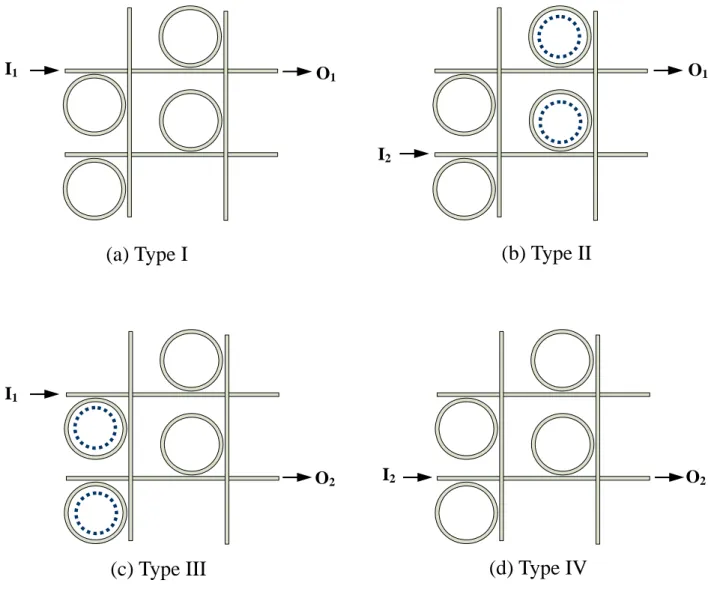
Input light with different wavelengths can be separated to either output ports according to their wavelengths. In this device, the corresponding output port can be selected externally. When a switch is in on the bar state, input light beam A connects to output light beam C, and input light beam B connects to output light beam D. When a switch is in the cross state, the connections are from input A to output D and input B to output C. These states are controlled by several different voltages applied to the several electro pad regions such as Fig. 4-2 shows. The mark of“I"means the input light signal、the mark of“O"means the output light signal、the mark of“D"means the drop light signal and the lower mark “number"
means the port number. As Fig. 4-2 shows, our signal will directly pass through the output port without adding any voltage on electro pads as Fig.
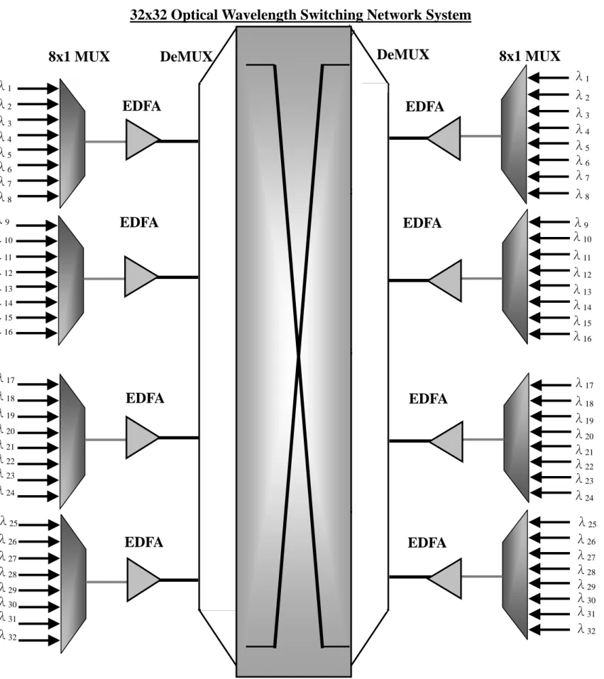
4-2-(a) and Fig. 4-2-(d) shows. With adding the voltages on the several electro pads to tuning the refractive index of the two microrings, we can modulate the light signal from input1 or input2 to arbitrary output port such as Fig. 4-2-(b) and Fig. 4-2-(c) show. Due to cascade our designed 2×2 SOI microring resonator to the network topology, we have the way to change the transmission state. That is, we take advantage of tuning the single microring refractive index to be on resonance state, the signal light routing to downward or upward. Based on the designed parameter in chapter 2 and chapter 3, we use those parameters to apply in the 32×32 optical wavelength switching network system as Fig. 4-3 shows. In our designed 32×32 optical wavelength switching system network , it were included of 32 different wavelength input that is for ITU standard 0.4nm spacing、4 pair
of 1×8 mutiplexer、one 4×32 demutiplexer and 4 EDFA in the input stage.
The output element stage is also similar to the input stage. Four characteristics for optical network performance are such as: optical path loss、 signal-to-noise ratio (SNR)、waveguide crossovers and number of switching elements. Optical switches play a key role in routing and the other function in advanced optical networks, both for dense-wavelength-division-multiplexed (DWDM) and single- wavelength applications [118-120]. Many optical switches based on SOI, SiGe, and LiNbO3 had been published in some literatures [121-122]. Due to the CMOS electronic device can reach gigabits-per-second logic optical switch array can achieve on SOI wafer. The optical phase modulators are designed in SOI optical switch very recently [123-127].
Recently, various switches based on microring have been reported in literatures [128-130]. Microring have several advantages of low cross talk、
high quality factor、wide FSR and compact .The free spectral range (FSR) of the ring is the separation between two resonant wavelengths. When using a DWDM system with a large number of channels, the FSR of the ring must be sufficiently large to select only a single channel. As the FSR is inversely proportional to the circumference length, with these low bend losses, ring and racetrack resonators become possible. According to the above literature, we can add switching voltages to change the localized refractive index. The resulting localized refractive index change caused the light output to switch from one side of the device to the other.
4-2 Mathematical Formulation of Optical Switching Network with Different Kind Switching Architecture
Several architectures for larger capacity networks have been proposed, among them: crossbar [131], planar [132-134], tree [135-139], Clos and Benes [140], as well as their dilated version [141]. Various optimization approaches to photonic networks [142] were focused on one or a combination of the following parameters: number of switch elements, number of crossovers [143], control complexity, device length, number of electronic driver, broadcast requirements, and others. In this section, we would carry in the SNR theory model and path loss formulation of optical cross-connect base on 2×2 optical microring routing wavelength switching element by our designed network architecture. Then we will also illustrate the SNR and path loss formulation of each kind network structure. Finally, we would compare the performance of each network structure in the next section.
4-2-1 Mathematical Formulation of Photonic Switching Architecture , such as Crossbar、Double Crossbar、N–Stage Planer Network
Based on the technology for guided-wave switching, several switching architectures have been proposed for optical space switching networks.
These architectures include the cross-bar, double-crossbar, N-stage planar, networks. In the following sections, "L" dB represents the loss in every
switch. In the following discussion, we will follow this view, referring to switch crossover when talking about SXR. The SXR of each switch is represented by " X " dB. The crossbar architecture is the most commonly used in electric switching. The major problem with the crossbar architecture is that connections have different attenuation because they use a different number of switching elements. An N×N crossbar network requires N2 beta elements, and the worst case of attenuation is
Path loss = (2N-1)L dB (4-2-1) The worst case is signal-to-noise ratio is
SNR = X -10log10(N-1) dB (4-2-2) There is no waveguide crossover. The crossbar architecture is shown in Fig.4-4. The second structure is Double Crossbar: To improve the performance of the crossbar architecture, Kondo introduced the double crossbar in 1985 [144]. The double-crossbar architecture not only reduces the path loss and increases the SNR, but also solves the problem of different paths having different attenuation in the crossbar. An N×N double-crossbar network needs 2N2-switching elements.
The path loss is:
Path loss = (N+1)L dB (4-2-3) The signal-to-noise ratio is
SNR = 2 X -10 log10(N-1) dB (4-2-4) The maximum number of waveguide crossovers is
W = N(N-1) (4-2-5) The Double crossbar architecture is shown in Fig.4-5. The third structure is N-Stage Planar structure. The N-stuge planar network is a rearrangeably nonblocking network that was proposed by Spanke and Benes in 1987 [138]. An N×N N-stage planar network has N(N-1)/2 switching elements.
The worst case path loss of the network is
Path loss = (N)L dB (4-2-6) The signal-to-noise ratio is
SNR = X -10log10(N) dB (4-2-7) There is no waveguide crossover.
The N-stage Planar architecture is shown in Fig.4-6.
4-2-2 Mathematical Formulation of Photonic Switching Architecture , such as Benes、Dilated Benes、AS/AC Network
The following structure is Benes structure. The Benes networks [145], this network requires the fewest switching elements and has the lowest attenuation. There is no difference in path loss between any connections.
The major problem with using the Benes network is the control algorithm.
An N×N Benes network needs (2log2N-1)N/2 switching elements. The path loss of the network is
Path loss = (2log2N-1)L dB (4-2-8) And the signal-to-noise ratio is
SNR = X -10log10(2log2N-1) dB (4-2-9) The maximum number of waveguide crossovers is
W=2N-2log2N-2 (4-2-10) The Benes architecture is shown in Fig.4-7. Following is the Dilated Benes structure: Because the crosstalk (SNR) of the 2x2 switching elements limits the size of the Benes network, Padmanabhan and Netravali modified the Benes architecture in 1987 [139]. It was called the dilated Benes network.
Dilated network architecture is based on the restriction that no switching elements carry more than one active path simultaneously. In such architectures, only one input and output of each switching element is used.
The number of the switching to 2Nlog2N. The path loss of the network is
Path loss = (2log2N)L dB (4-2-11) The signal-to-noise ratio is
SNR = 2 X -10log10(2log2N-1) dB (4-2-12)
The maximumnumber of waveguide crossovers is
W = 4N-2log2N-5 (4-2-13) The Dilated Benes architecture is shown in Fig.4-8. Finally is Active Splitter and Active Combiner (AS/AC): Spanke introduced The AS/AC architecture, in 1986 [137]. The 1×N active splitter and the N×1 active combiner are two basic components of an N×N AS/AC network. All of the possible signal paths in this network have the same path loss. The path loss of an N×N AS/AC network is
Path loss = (2log2N)L dB (4-2-14) The worst case signal-to-noise ratio is
SNR = 2 X -10log10(log2N) dB (4-2-15) The maximum number of waveguide crossovers is
W = (N-1)2 (4-2-16) The Active Splitter and Active Combiner architecture is shown in Fig.4-9.
We will use our designed microring resonator applied to those network architectures. In next section, we would like to compare each of the structures by SNR and path loss.
4-3 Analysis of Application Integrated Optical Switching
Network Based on Microring Resonator
In this section, I will show the performance of these kinds of network architecture for the path loss、crosstalk、SNR、and number of switching elements. Besides, I also compared and analyzed those switching network based on the microring resonator. Based on the above section that derived related formulations for the switching network, it will be applied on the optical telecommunications. The propagation loss through the cross junction of the switching network is considered the primary loss of the network. The cross junction loss at our designed network is about -12dB.
The estimated cross junction loss is directly proportional to the channel number of optical microring switching network through which the optical path passes. Besides, the important issue is the coupling loss of the microring resonator which is on resonance. In our simulation device, there is 1.3874dB loss in one resonance resonator on average. The 2×2 switch device have 2.79 dB loss on average for devices. This number varies depending on the refractive index contrast 、 Polarization mode 、 semiconductor process by surface roughness and the displacement between the microring and the straight waveguide. The other parameter we must point out is SNR. SNR is a measure of the optical crosstalk that occurs when two signals interact with each other. Switch crossover is traditionally regarded as the major reason for the noise occurrence. In the following discussion, we will follow this view, referring to switch crossover when talking about SXR. The SXR of each switch is represented by " X " dB, which is 30dB for our 2×2 switching device. Loss of our designed 2×2 switching device “L“ is 2.79dB Waveguide Crossover: Although these values of results reported show that keeping the intersection angles above a certain minimum amount makes the crosstalk from passive intersections of
optical waveguides negligible [153], the number of waveguide crossovers in a network is another measure of the performance of the network.
Fig.4-10 shows the optical path losses of comparing various switching networks applying our designed 2×2 microring resonator switch at Gap = 125nm. Here we compared the path loss for six networks structure and we found that the Benes structure has the lowest path loss below 20 dB. The Double Crossbar and Crossbar structure have bigger path loss larger than 50 dB when the port number is increased than 16. Fig.4-11 shows the signal-to-noise ratio of comparing various switching networks that apply our designed 2×2 microring resonator switch at Gap = 125nm. Here we compared the SNR for six networks structure and we found that the Benes and AS/AC structure have the highest SNR ≧ 60 dB. The Double Benes and N-stage structure have lower SNR smaller than 30 dB. Fig. 4-12 shows the optical path losses of comparing various switching networks applying our designed 2×2 microring resonator switch at Gap = 150nm. From chapter 2 and chapter 3s` simulations we know that the coupling efficient is related closed to the path loss and signal-to-noise ratio. The path loss of those network structure as the gap size = 150nm is increased 5dB than the gap size =125nm as Fig. 4-10 shows. Also, the SNR of the six network structure when the gap size = 150nm decreased about 15 dB than the gap size= 125nm as Fig. 4-13 shows. Therefore, we want to know how much the coupling efficient effect the switching network performance. Because the Dilated Benes structure is the appropriate structure applying for our designed structure in previous discussion so we take in to analysis to the performance of the path loss and SNR individually. Fig. 4-14 shows comparison of path loss for Benes switching network structure applying our designed 2×2 microring resonator switch at various coupling coefficient from κ=0.65,0.6,0.55,0.5. From this figure we can observe that
the path loss is inverse proportional to the coupling coefficient. From Fig.
4-15 shows, The SNR is proportion to coupling coefficient. When κ=0.65 the SNR average at 60 dB, but when κ=0.5 the SNR average at 35 dB and the performance is getting worst.
Number of Switching Elements: The number of switching elements is a measure of the cost of the network. If more optical switching device is fabricated, then more separate driver amplifiers are needed. We give the comparison to Number of waveguide crossovers for various networks in Fig. 4-16. When the port number is 64, the waveguide crossover is larger then 100. But for our designed network structure, the number of waveguide crossover is 2. Finally, we compare the SNR of our designed network architecture to other various structures. From Fig.4-17, the SNR of our designed network structure is smaller than AS/AC、Benes and Double crossbar but larger than Dilated Benes、N-stage and Crossbar structure.
4-4 Discussion and Conclusions
According to the analysis of switching network structures in this chapter, the author will make some discussions and conclusions in follow texts.
In this chapter, we focus on the performance to various kind of structure by our designed 2×2 optical routing wavelength switch based on microring resonator. The new technology of router was also developed. We use our designed tunable 2×2 optical routing wavelength switch applied to
We analyzed the SNR and Path loss for those network structure. We also analyzed the coupling coefficient influence the switching performance. The novel network topology was also developed and analyzed. We found that, the advantage to use the microring resonator which serve as the routing component were those: high SNR、compact size、easy to integrate on chip.
Especially clearly play an enabling role in realizing future dynamic optical networks. Finally, we could apply such a device into optical network to save the finite channel wavelength numbers. For nonuniform traffic, dynamic reconfiguration of the wavelength routing interconnections is required in response to changing traffic patterns. Dynamic wavelength routing can be realized by introducing optical space switches at the wavelength routing nodes.
Fig. 4-1 The state of the 2×2 microring optical routing wavelength switch (a) Bar state
A
B
C
D E
F (b) Cross state
A
B
C
D E
F crosstalk
crosstalk crosstalk
I1
O2 I2 O2
(b) Type II
(d) Type IV
I1 O1
I2
O1
(a) Type I
(c) Type III
Fig. 4-2 Four types of single input configuration of the 2×2 microring optical routing wavelength switch
Fig. 4-3 The Bidirectional optical cross-connect schematic diagram of cascade-able 32×32optical wavelength switching with microring
λ8
λ1
λ2
λ3
λ4
λ7
λ6 λ5
λ9
λ10 λ11 λ12
λ15
λ14
λ16
λ13
λ17
λ18
λ19
λ20
λ23
λ22
λ24
λ21
λ25
λ26
λ27
λ28
λ31
λ30
λ32
λ29
EDFA EDFA
EDFA EDFA
λ1 λ2 λ3 λ4
λ7 λ6 λ5
λ9 λ10
λ11 λ12
λ15
λ14
λ16
λ13
λ17 λ18 λ19 λ20
λ23 λ22
λ24 λ21
λ25
λ26
λ27 λ28
λ31
λ30
λ32 λ29
λ8
EDFA EDFA
EDFA EDFA
DeMUX DeMUX 8x1 MUX
8x1 MUX
32x32 Optical Wavelength Switching Network System
1
2
N
1 2 N Fig.4-4 The structure of crossbar network
……
……
Output Channels Input
Channels 1
2
1
2
Fig.4-5 The structure of double-crossbar network
1 2 3 4 5 6
1 2 3 4 5 6
Fig.4-6 The structure of N-stage planar network
1 2
3 4
5 6
7 8
1 2
3 4
5 6
7 8
Fig.4-7 The structure of Benes network
Fig.4-8 The structure of dilated Benes network 1
2
3
4
1
2
3
4
1
2
3
4
1
2
3
4
Fig.4-9 The structure of Active Splitter/Active Combiner (AS/AC)
0 8 16 24 32 40 48 56 64 0
10 20 30 40 50
5 15 25 35 45
Network architecture Crossbar Double Crossbar N-Stage Planer Benes Dolated Benes AS/AC
Channel number
Path Loss (dB)
0 8 16 24 32 40 48 56 64
0 10 20 30 40 50 60 70 80
Network architecture Crossbar Double Crossbar N-Stage Planer Benes Dolated Benes AS/AC
Signal to Noise Ratio (dB)
Channel number
Fig.4-10 Optical path losses of comparing various switching networks applying our designed 2×2 microring resonator switch at Gap = 125nm
Fig.4-11 Comparison of SNR for various switching networks of comparing various switching networks applying our designed 2×2 microring resonator switch at Gap = 125nm
0 8 16 24 32 40 48 56 64 0
10 20 30 40 50
5 15 25 35 45
Network architecture Crossbar Double Crossbar N-Stage Planer Benes Dolated Benes AS/AC
Channel number
Path Loss (dB)
0 8 16 24 32 40 48 56 64
0 10 20 30 40 50 60 70
80 Network architecture
Crossbar Double Crossbar N-Stage Planer Benes Dolated Benes AS/AC
Channel number
Signal to Noise Ratio (dB)
Fig.4-12 Optical path losses of comparing various switching networks
applying our designed 2×2 microring resonator switch at Gap = 150 nm
Fig.4-13 Comparison of SNR for various switching networks applying our designed 2×2 microring resonator switch at Gap = 150nm
8 16 24 32 40 48 56 64
4 12 20 28 36 44 52 60
30 40 50 60 70
35 45 55 65
Coupling coefficient K=0.65 k=0.6 K=0.55 K=0.5
Fig.4-15 Comparison of SNR to Benes switching network structure with different coupling coefficient
Fig.4-14 Comparison of path loss for Benes switching network structure applying our designed 2×2 microring resonator switch at various coupling coefficient
Channel number
Signal to Noise Ratio (dB)
Channel number
Path loss (dB)
8 16 24 32 40 48 56 64
4 12 20 28 36 44 52 60
0 10 20 30
5 15 25
Network structure k=0.65 K=0.6 K=0.55 K=0.5
8 16 24 32 40 48 56 64
4 12 20 28 36 44 52 60
0 100 200 300 400 500
50 150 250 350 450
Networks Architecture Crossbar Double Crossba N-Stage Planer Benes Dilated Benes
0 8 16 24 32 40 48 56 64
0 10 20 30 40 50 60 70 80
Network architecture Crossbar Double Crossbar N-Stage Planer Benes Dolated Benes AS/AC
Our designed structure
Number of Waveguide crossover
Channel number
Channel number
Signal to Noise Ratio (dB)
Fig.4-17 Comparison SNR of our designed network architecture to other various switching network structure
Fig.4-16 Comparison to Number of waveguide crossovers for various networks
Our design switching network