行政院國家科學委員會專題研究計畫 成果報告
深次微米金氧半場效電晶体高頻雜訊特性及其在電晶体小 訊號等效電路應用之研究
計畫類別: 個別型計畫
計畫編號: NSC91-2215-E-011-004-
執行期間: 91 年 08 月 01 日至 92 年 07 月 31 日 執行單位: 國立臺灣科技大學電子工程系
計畫主持人: 張勝良
報告類型: 精簡報告
處理方式: 本計畫可公開查詢
中 華 民 國 92 年 10 月 27 日
深次微米金氧半場效電晶体高頻雜訊特性及其在電晶体小訊號等效電路應用之研究
High-Frequency Noise Property of deep submicron MOSFET and its application in small-signal equivalent circuits
計畫編號:NSC 91-2215-E-011-004 執行期限:91 年 08 月 01 日至 92 年 07 月 31 日 主持人:張勝良 執行機構及單位名稱 台灣科技大學
E-mail:sljjj@et.ntust.edu.tw 一、中文摘要
這個計畫的目的是研究深次微米金氧半場效電晶體的高頻雜訊及其在小訊號電路模型的應 用。這個非區域化通道熱雜訊模型能夠預測金氧半場效電晶體的高頻熱雜訊與汲極閘極偏壓 及通道長度的關係。本模型的正確經由實驗得到驗證。
關鍵詞:深次微米金氧半場效電晶體,高頻雜訊,熱雜訊,模擬研究。
Abstract
This report presents a new quasi-2-D nonlocal channel thermal noise model for nMOSFET's, which can simulate the channel thermal noise of MOSFETs at different Vgs/ Vds biases and with channel lengths down to deep submicron. The apparent short-channel effect, hot-carrier effect and nonlocal carrier dynamics reflect not only in the drain, substrate and gate currents but also in the channel current noise. In the model, first, the moblity and inversion layer areal charge density are calculated from the current-voltage model presented previously. Then the channel electric field is calculated and the nonlocal electron temperature is generated. Finally, the channel thermal noise is calculated based on the presented model with the nonlocal electron temperature, and a comparison between the modeled and measured data is carried out to show the accuracy of the model.
Keywords: MOSFET, thermal noise modeling, hot electron, non-local effect.
二、緣由與目的
With the very high unity-gain frequency of deep submicron MOSFETs of more than 100GHz [1], many high-speed and RF ICs are likely to be implemented in CMOS technology.
because of its low cost and high level of integration. At low frequency, the MOSFET device noise is mainly dominated by flicker noise (1/f noise ), which is up-converted to affect the phase noise of RF circuits such as VCOs. However, at high frequency it is dominated by the thermal noise, which within the channel gives rise to both drain channel noise and induced gate noise [2]. Accurate modeling of high frequency noise is a prerequisite for the application of modern CMOS technologies to low-noise RF circuits such as low-noise amplifier, mixer and oscillators.
In the past, there have been several thermal noise models published for MOSFETs. The drain thermal noise of long channel MOSFETs agrees with the Van der Ziel model[3] while in a number of publications, a considerably enhanced thermal noise in submicron and deep-submicron MOSFETs have been reported [4]-[7]. In analog integrated circuits MOS transistor is usually biased in saturation region, where the strong lateral electrical field causes short-channel devices to show different current-voltage characteristics behavior and
enhanced drain current thermal noise in comparison to long-channel devices. P-channel MOSFETs also show enhancement although somewhat smaller than n-channel MOSFETs. The device simulations also seem to confirm these results[8].
Some modeling works [9], [10] explained the enhanced thermal noise of scaled-down MOSFETs using local field approach, where the electron temperature is a function of local channel electrical field. The local approach can not exactly describe the device physics of modern MOSFETs. To account for the nonlocal carrier transport effect which frequently occurs in modern MOSFETs, on the other hand, hydrodynamic formulation based on 2-D device simulator[11] was used to calculate channel thermal noise. The 2-D numerical simulation method[11] although can be used to accurately calculate thermal noise, it is time consuming and is unfriendly for characterizing high frequency noise parameters. In this paper, we, therefore, present a nonlocal thermal channel noise model to describe the thermal noise behavior. This model can be used to characterize measured noise data and also show nonlocal thermal noise behavior, it is capable of simulating the channel thermal noise of submicron/deep-submicron MOSFET devices operated in both the triode and saturation regions. The accuracy of this model is verified by comparision with measured data. This thermal model in conjunction with our previous MOSFET current model[12] forms a useful quasi two-dimensional model for studying modern MOSFETs.
三. 研究方法及成果
In this section, we develop a nonlocal model for the channel thermal noise, which was originated by Aldert van der Ziel[3]. The detailed theory can be found in [13].
Figure 1 shows the thermal noise with the change of VGS under VDS =0.1 V while the MOSFET is biased in the linear region. Fig. 2 shows the thermal noise with the change of VGS under VDS = 2.5 V while the MOSFET is biased in the saturation region. The width/length of the MOSFET in both Figs. 1 and 2 is 96um/0.25um, and is made by 0.25 um technology.
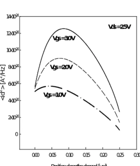
Fig. 3 shows the simulated channel thermal noise at three biases. In source-side channel the thermal noise increases along the channel due to the increase of electron temperature, however in the drain-side channel it decreases along the channel due to the decrease of inversion charge density. Since the trend of the inversion layer areal density is falling down and the electron temperature T is climbing up drastically along the channel, the multiplication of the above two effects results in a peak thermal noise contribution from mid channel region.
The increase in electron temperature in drain-side channel tends to increase the value of overall thermal noise as channel length shrinks and drain bias increases.
To see the nonlocal temperature effect on the channel thermal noise, in Fig. 4 we compare the modeled results with and without nonlocal effect (T = 300K) to the measured channel thermal noise. The results show clearly that the channel thermal current noise increases drastically with the decrease in channel length, this is attributed to the inceased hot-electron effect at small channel length. The increasing electrical field causes more carrier to gain higher energy thus increasing electron temperature and the amount of channel thermal noise near the drain. The modeled data show that the theory without nonlocal electron temperature effect predicts less thermal current noise. Comparing with the experimental data of Klein's [7], our model gives a good agreement.
四、結果與討論
We have developed a nonlocal channel thermal current noise model for both submicron and deep-submicron nMOSFETs. This model incorporates the nonlocal electron temperature in the formulation of channel thermal noise, and the modeled results agree with the experimental channel thermal noise of devices operated both in the linear and saturation regions and with various channel widths and lengths. The present model can show the distribution of thermal noise distribution along the channel, and it gives device physics insight on the variation of channel thermal noise versus channel length, gate bias, and drain bias, it also leads to a better understanding about the device physics of measured channel thermal current noise.
五、參考文獻
[1]T. Manku, "Microwave CMOS-device physics and design," IEEE J. Solid State Circuits, vol 34, pp.277-284, March 1999.
[2] C. H. Chen and M. J. Deen, "High frequency noise MOSFETs modelling,"
Solid State Electron., vol 42, pp. 2069-2081, 1998.
[3]Aldert van der Ziel, Noise in Solid State Devices and Circuits. New York:Wiley,1986
[4]R. P. Jindal, "Hot-electron effects on channel thermal noise in file-line n-MOS field-effect transistors," IEEE Trans. Electron Devices, vol. ED-33. pp.1395-1397, Sept, 1986.
[5]S. Tedja, J. Van del Spiegel, and H. Williams, "Analytical and
experimental studies of thermal noise in MOSFETs," IEEE Trans. Electron Devices, vol 41, pp. 2069-2075, Nov. 1994.
[6]A. A. Abidi, "High-frequency noise measurements on FETs with small
dimensions," IEEE Trans. Electron Devices, vol. ED-33, pp. 1801-1805, Nov.1986.
[7]P. Klein, "An analytical thermal noise model of deep-submicron MOSFET's," IEEE Electron Device Lett., pp. 399-401, 1999.
[8]A. J. Scholten, H. I. Tromp, L. E. Tiemeijer, R. van Langevelde, R.
J. Havens, P. W. H. de Vreexte, R. F. Woerlee, A. H. Montree,and D. B. M.
Klaassen, "Accurate thermal noise model for deep-submicron CMOS," IEDM99-155.
[9]D. Triantis, A. Birbas,and D. Kondis, "Thermal noise modeling for short channel MOSFETs,"
IEEE Trans. Electron Devices, vol 43, pp. 1950-1955, Nov. 1996.
[10] G. Knoblinger, P. Klein, M. Tiebout, "A new model for thermal channel noise of deep-submicron MOSFETs and its application in RF-CMOS design," IEEE J. Solid-State Circuits.
vol 36, no. 5, pp.831-836, May 2001.
[11] J.-S. Goo, C.-H. Choi,A. Abramo, J.-G Ahn, Z. Yu, T. H. Lee, and
R. W. Dutton, "Physical origin of the excess thermal channel noise in short MOSFETs,"
IEEE Electron Device Letts., vol 22, pp. 101-103, 2001.
[12]C.-J. Sheu and S.-L. Jang, " A MOSFET gate current model with the direct tunneling mechanism, " Solid-State Electron. 44,
pp.1819-1824, 2000.
[13]H.-F. Teng and S.-L. Jang, " A nonlocal channel thermal noise model for nMOSFETs, "
Solid-State Electron. 47, pp.815-819, 2002.
六、圖表
Fig. 1 Fig. 3
Fig. 2 Fig. 4
Vgs [V]
0.5 1.0 1.5 2.0 2.5
<id2> [A2/Hz]
0 2 4 6 8 10 12 14 16 18 20
measured data [10]
our model
Vds = 2.5 V W/L = 96um/0.25um 0.25 um Technology
Vgs [V]
0.5 1.0 1.5 2.0 2.5
<id2> [A2/Hz]
0 2 4 6 8 10 12 14 16 18
measured data [10]
our model
Vds = 0.1 V W/L = 96um/0.25um 0.25 um Technology
Fig. 1 Comparison between the channel thermal noise model with measured data for a 0.25-um nMOS in the linear region.
Channel length [ um ]
0 1 2 3 4
< id > [ pA / (Hz)1/2 ]
0 2 4 6 8 10 12 14
measured data [ 7 ] model with nonlocal effects model with T = 3000K
Position along the channel [um]
0.00 0.05 0.10 0.15 0.20 0.25 0.30
<id2> [A2/Hz]
0 2x10-24 4x10-24 6x10-24 8x10-24 10x10-24 12x10-24 14x10-24
Vgs = 2.0 V
Vgs = 1.0 V Vgs = 3.0 V
Vds = 2.5 V