Single-crystalline AlZnO nanowires/nanotubes synthesized at low temperature
Ruey-Chi Wang, Chuan-Pu Liu,a兲and Jow-Lay Huang
Department of Materials Science and Engineering, National Cheng Kung University, Tainan 70101, Taiwan and Center for Micro/Nano Science and Technology, National Cheng Kung University,
Tainan 70101, Taiwan Shu-Jen Chen
Department of Chemical and Material Engineering, National Kaohsiung University of Applied Sciences, Kaohsiung 80778, Taiwan
共Received 19 August 2005; accepted 2 November 2005; published online 11 January 2006兲 Single-crystalline AlZnO nanomaterials were synthesized through a proposed alloy-evaporation deposition method at the low temperature of 550 ° C by thermal chemical vapor deposition.
Transmission electron microscopy images show that AlZnO nanowires, or nanowire/nanotube junction structures, can be synthesized where the Al/共Al+Zn兲 atomic ratio is determined to be about 2.5 and 12 at. %, respectively, by electron energy loss spectrometry. Room-temperature cathodoluminescence measurements show that the AlZnO nanowires exhibit a strong ultraviolet emission, which shifts to a higher energy from 3.29 to 3.34 eV due to Al incorporation. © 2006 American Institute of Physics. 关DOI:10.1063/1.2161393兴
Recently, ZnO has attracted much research attention ow- ing to its special optoelectrical properties for the direct wide band gap of 3.37 eV and large exciton binding energy of 60 meV at room temperature, which also makes ZnO one of the most promising candidates for nanodevices. To enhance electrical and optical properties, ZnO films were frequently doped or alloyed with group II, III, IV, V, and VI elements.
Of these, Al:ZnO could reach the highest conductivity with- out deteriorating the optical transmission, and thus has been highly regarded as a potential alternative to the most ac- cepted transparent conductive material, indium-tin oxide.1 However, although ZnO nanomaterials doped or alloyed with Ga,2–4In,4 Sn,4 Co,5 Ni,5 Cd,6 Mg,7–9Pb,10and S 共Ref. 11兲 have been reported, the synthesis of Al:ZnO or AlZnO nano- structures still remains challenging due to the high oxidation reactivity of Al sources and a tremendous difference in vapor pressure between Zn and Al.
In the letter, we report on the synthesis of single- crystalline AlZnO nanostructures by a proposed alloy- evaporation deposition method. By means of controlling the alloying treatment of sources at various temperatures above the eutectic point of the Zn–Al binary phases prior to the nanowire growth, either AlZnO nanowires or nanowire/
nanotube junction structures with various Al concentrations could be synthesized at a low temperature of 550 ° C without additional treatments. Cathodoluminescence 共CL兲 results show that the AlZnO nanowires exhibit strong ultraviolet 共UV兲 emission, which shifts to a shorter wavelength due to Al incorporation.
The AlZnO nanostructures were synthesized via an alloy-evaporation deposition method on ITO film coated glass substrates. Zn 共purity: 99.8%, 100 mesh兲 and Al 共pu- rity: 99.9%, 100 mesh兲 mixed powder 共weigh ratio=93:7兲 were placed in an aluminum boat located inside a 1 in. di- ameter horizontal quartz tube reactor. Neither catalysts nor
additives are needed. A 1 mm gap was set between the sources and the substrate. The sources were heated at a rate of 20 ° C / min from room temperature to an alloying treat- ment temperature. Argon was introduced as the carrier gas in the beginning with a flow rate of 8 sccm and the working pressure was kept at 100 Torr. The alloying treatment for the AlZnO nanostructures was carried out at either 420 ° C or 500 ° C for 10 min. After the alloying treatment, the pressure was decreased to 1 Torr, and the system was heated again at a rate of 20 ° C / min to 550 ° C. Once the temperature was raised to 550 ° C for 3 min, oxygen was introduced into the chamber with a flow rate of 1 sccm. After heating at 550 ° C for 60 min, the substrate was slowly cooled down in the furnace. The as-prepared nanostructures were then examined by field-emission scanning electron microscopy 共FE-SEM兲 with JEOL 6700F, field-emission transmission electron mi- croscopy共FE-TEM兲 with JEOL 2100F for morphology, CL, microstructure, and composition. The CL spectra were com- pared with those from pure ZnO nanowires.12
Because the Al vapor pressure is much lower than Zn by 10−12order at the same temperature range, it is difficult to achieve an adequate Al concentration by directly mixing Al and Zn sources on an additive rule basis. However, by means of a concept of alloying Zn and Al sources as the first step in the process, an adequate quantity of Al vapor can be estab- lished easily even at low temperatures of 420– 500 ° C for the subsequent growth of nanomaterials after the formation of a certain quantity of Zn–Al alloy by interdiffusion through the Zn/ Al interface. The vapor pressures of the Zn–Al alloy liquid共VZn–Al兲 and the Zn liquid 共VZn兲 are functions of tem- perature and composition and contribute to the growth of AlZnO nanostructures according to
Vtotal= AZnVZn+兺i AiZn–AlViZn–Al, 共1兲
where V denotes the vapor pressure, while A is the area ratio of evaporation, and i is the component of each alloy constitu- ent for the composition variation in the alloy.
a兲Author to whom correspondence should be addressed; electronic mail:
APPLIED PHYSICS LETTERS 88, 023111共2006兲
0003-6951/2006/88共2兲/023111/3/$23.00 88, 023111-1 © 2006 American Institute of Physics
Downloaded 15 Oct 2006 to 140.116.134.115. Redistribution subject to AIP license or copyright, see http://apl.aip.org/apl/copyright.jsp
Figure 1共a兲 shows FE-SEM images of the AlZnO nanowires synthesized using the alloying treatment at 420 ° C. The nanowires exhibit straight and sharp morphol- ogy with abrupt shrinkage in diameter from 200– 300 nm to 15– 20 nm. The length of the finer portion of a nanowire is around 2m, and its aspect ratio is as large as 100–130. Figure 1共b兲 shows the AlZnO nanowire/
nanotube junction structures synthesized using the alloying treatment at 500 ° C. The nanostructures show gradual shrinkage in diameter from 200– 300 nm to 50– 70 nm at the top. An enlarged view of the open-ended nanotube morphol- ogy is shown in the inset of Fig. 1共b兲. Close-ended nanotubes were also found.
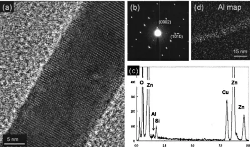
Figure 2共a兲 shows a high-resolution FE-TEM image of a nanowire fabricated using the alloying treatment at 420 ° C.
The diameter of the nanowire is around 15 nm, which repre- sents the upper half of the nanowire in the FE-SEM image of Fig. 1共a兲. Figure 2共b兲 is an electron diffraction pattern of the nanowire, which indicates that the nanowire is a single- crystalline structure grown along the关0001兴 direction. The energy-dispersive x-ray spectrum in Fig. 2共c兲 shows that the nanowire consists of Zn, O, and Al, where Cu and Si could be attributed to the Cu grid and C holey film. Figure 2共d兲 is the Al map from L edge at 73 eV for the nanowire derived by the three-window technique in electron energy-loss spec- trum共EELS兲, suggesting that Al atoms distribute uniformly over the nanowire. The atomic ratio of Al to共Al+Zn兲 in the nanowires is calculated to be around 2.5 at. %.
Figure 3共a兲 shows a low-magnification transmission electron microscopy 共TEM兲 high-angle annular dark-field 共HAADF兲 image of a nanotube fabricated using the alloying treatment at 500 ° C, clearly demonstrating the hollow char-
acteristics of the nanotube from Z contrast. The nanotube nucleated at the necking region of a nanowire and an en- larged bright-field image of the nanotube is shown in Fig.
3共b兲. The thickness of the wall region is around 15 nm while the diameter of the hollow core region is about 30 nm. Fig- ures 3共c兲 and 3共d兲 show the high-resolution FE-TEM image and electron diffraction pattern of the interface, respectively, from the box area in Fig. 3共b兲, indicating that the nanotube is a single-crystalline structure grown along the关0001兴 direc- tion. An enlarged view of the necking area in Fig. 3共e兲 shows faceted features of another nanotube. The Al elemental map in Fig. 3共f兲 shows a higher Al signal than the one in Fig. 2共d兲 and some inhomogeneity of Al distribution. The atomic ratio of Al to共Al+Zn兲 in the nanotube calculated from the EELS spectrum is around 12 at.%. In addition, the elemental maps of Zn and O 共not shown兲 show uniform distribution. The thickness map by EELS is shown in Fig. 3共g兲. Figure 3共h兲 is a thickness profile from Fig. 3共g兲 showing the characteristics of a nanotube. Here, from these two nanostructures, we dem- onstrate that AlZnO nanomaterials can be synthesized by our proposed method and Al composition can be controlled and altered simply by varying the alloying treatment temperature.
Since no catalyst was used in the process, the growth of AlZnO nanostructures was not nucleated by the conventional vapor-liquid-solid mechanism. Instead, the nanostructures may nucleate via a self-catalyzed mechanism.13 The nano- tube nucleation at the necking region of a nanowire may be a result of lattice mismatch along the one-dimensional nano- structure. Examining the diffraction patterns along the c-axis direction, the reduction in the lattice constant of the nanotube compared with the connected nanowire is around 2%, which is caused by increased Al concentration in ZnO. The nano-
FIG. 1. Scanning electron microscopy images of 共a兲 AlZnO nanowires synthesized using the alloying treat- ment at 420 ° C.共b兲 AlZnO nanowire/nanotube junction structures synthesized using the alloying treatment at 500 ° C with the inset for an enlarged view of an AlZnO nanotube.
FIG. 2. TEM characterization of the AlZnO nanowires synthesized using the alloying treatment at 420 ° C: 共a兲 High-resolution image, 共b兲 electron diffraction pattern, 共c兲 energy- dispersive x-ray spectrum, and共d兲 Al elemental map determined by EELS 共L edge at 73 eV兲.
023111-2 Wang et al. Appl. Phys. Lett. 88, 023111共2006兲
Downloaded 15 Oct 2006 to 140.116.134.115. Redistribution subject to AIP license or copyright, see http://apl.aip.org/apl/copyright.jsp
structures grow in a tubelike shape rather than wirelike mor- phology to release the stress induced by lattice mismatch.
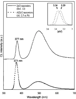
Figure 4 shows the room-temperature CL spectrum of the AlZnO nanowires共Al: 2.5 at. %兲 as in Fig. 1共a兲 with that of pure ZnO nanowires of similar sizes synthesized previously.12 Both spectra exhibit a relatively sharp UV emission and a broad green emission centered at around
500 nm. The UV emission is attributed to the near band-edge excitonic recombination, while the green emission may be the result of the transition between the photoexcited holes and singly ionized oxygen vacancies.14 The results indicate that the as-synthesized AlZnO nanowires possess high- crystal quality only with few oxygen vacancies. An enlarged view of the UV emission peaks after normalizing UV inten- sity is shown in the inset of Fig. 4. The UV peak position of the AlZnO nanowires shifts to a higher energy of 3.34 eV compared with 3.29 eV from the pure ZnO nanowires共Ref.
12兲. The results are consistent with the studies of Lee et al.15 on the optoelectronic properties of Al:ZnO films. The blue- shift of the UV peak indicates a broadening of band gap in agreement with the observation from the optical absorption measurements of Al:ZnO resulted from the Burstein–Moss effect.16 Compared with the AlZnO nanowires 共Al:
2.5 at. %兲, the CL spectrum 共not shown兲 of the AlZnO nanowire/nanotube junction structure 共Al: 12 at. %兲 as in Fig. 1共b兲 shows a similar result without further blueshift of the UV peak, indicating that effective doping effect can only be achieved with an appropriate Al composition in AlZnO nanomaterials, which can be controlled by our method.
In summary, single-crystalline AlZnO nanowires and nanowire/nanotube junction structures with various Al con- centrations were synthesized at a low temperature of 550 ° C via a proposed alloy-evaporation deposition method with dif- ferent alloying treatment procedures. The Al/共Al+Zn兲 atomic ratio in the ZnO nanowires and nanowire/nanotube junction structures determined by EELS is about 2.5 and 12 at. %, respectively. Room-temperature CL measurements show that the AlZnO nanowires exhibit a strong UV emis- sion, which shifts to a higher energy from 3.29 to 3.34 eV due to Al incorporation.
The work was supported by Research Grant No. NSC94- 2120-M-006-006, National Science Council of Taiwan.
1M. Chen, Z. L. Pei, X. Wang, C. Sun, and L. S. Wen, J. Vac. Sci. Technol.
A 19, 963共2001兲.
2J. Zhong, S. Muthukumar, Y. Chen, Y. Lu, H. M. Ng, W. Jiang, and E. L.
Garfunkel, Appl. Phys. Lett. 83, 3401共2003兲.
3C. Xu, M. Kim, J. Chun, and D. Kim, Appl. Phys. Lett. 86, 133107 共2005兲.
4S. Y. Bae, C. W. Na, J. H. Kang, and J. Park, J. Phys. Chem. B 109, 2526 共2005兲.
5J. B. Cui and U. J. Gibson, Appl. Phys. Lett. 87, 133108共2005兲.
6Q. H. Li, Q. Wan, Y. G. Wang, and T. H. Wang, Appl. Phys. Lett. 86, 263101共2005兲.
7Y. W. Heo, M. Kaufman, K. Pruessner, D. P. Norton, F. Ren, M. F.
Chisholm, and P. H. Fleming, Solid-State Electron. 47, 2269共2003兲.
8W. I. Park, S. J. An, J. L. Yang, G.-C. Yi, S. Hong, T. Joo, and M. Kim, J.
Phys. Chem. B 108, 15457共2004兲.
9M. Lorenz, E. M. Kaidashev, A. Rahm, T. Nobis, J. Lenzner, G. Wagner, D. Spemann, H. Hochmuth, and M. Grundmann, Appl. Phys. Lett. 86, 133107共2005兲.
10S.-M. Zhou, X.-H. Zhang, X.-M. Meng, S.-K. Wu, and S.-T. Lee, Phys.
Status Solidi A 202, 405共2005兲.
11S. Y. Bae, H. W. Seo, and J. Park, J. Phys. Chem. B 108, 5206共2004兲.
12R. C. Wang, C. P. Liu, J. L. Huang, S.-J. Chen, Y.-K. Tseng, and S.-C.
Kung, Appl. Phys. Lett. 87, 013110共2005兲.
13J. Q. Hu, Q. Li, N. B. Wong, C. S. Lee, and S. T. Lee, Chem. Mater. 14, 1216共2002兲.
14K. Vanhausden, W. L. Warren, C. H. Seager, D. R. Tallant, J. A. Voigt, and B. E. Gnade, J. Appl. Phys. 79, 7983共1996兲.
15H. W. Lee, S. P. Lau, Y. G. Wang, K. Y. Tse, H. H. Hng, and B. K. Tay, J.
Cryst. Growth 268, 596共2004兲.
16E. Burstein, Phys. Rev. 25, 7826共1982兲.
FIG. 3. TEM characterization of the AlZnO nanowire/nanotube junction structures synthesized using the alloying treatment at 500 ° C:共a兲 Medium- magnification HAADF image,共b兲 high-magnification bright-field image, 共c兲 high-resolution image,共d兲 electron diffraction pattern, 共e兲 bright-field image of the necking area,共f兲 Al elemental map determined by EELS 共L edge at 73 eV兲, 共g兲 thickness map, and 共h兲 thickness profile across the line in Fig.
4共g兲.
FIG. 4. Room-temperature CL spectra of the AlZnO nanowires 共Al:
2.5 at. %兲 synthesized using the alloying treatment at 420 °C and pure ZnO nanowires synthesized in previous work 共Ref. 12兲 with the inset for an enlarged view of the UV peaks after normalizing the intensity.
023111-3 Wang et al. Appl. Phys. Lett. 88, 023111共2006兲
Downloaded 15 Oct 2006 to 140.116.134.115. Redistribution subject to AIP license or copyright, see http://apl.aip.org/apl/copyright.jsp