國立臺灣大學工學院材料工程學系 博士論文
Graduate Institute of Materials Engineering College of Engineering
National Taiwan University Doctoral Dissertation
高鉛/銅與高鉛/鎳液固反應中之大規模剝離現象 Study of massive spalling in high-Pb/Cu and
high-Pb/Ni soldering reactions
蔡孟宏 Meng-Hong Tsai
指導教授:高振宏 博士 Advisor: C. Robert Kao, Ph.D.
中華民國 99 年 7 月
July, 2010
Acknowledgements
作者十分感謝指導教授高振宏老師,在研究領域上的耐心指導;並如慈父般 的鼓勵與幫助;更無私地分享生活經驗與處世態度。
作者也十分感謝吳子嘉教授;劉正毓教授;顏怡文教授;羅偉誠博士;陳智 教授;陳志銘教授,能在百忙之中對於本研究的內容,給予專業的建議與指導。
作者也十分感謝實驗室的夥伴們,在實驗與生活上的幫助,感謝彥良;建偉;
素純;育蔚;明諺;智強;儀雯;明弘;承翰;欣楷;鑫毅;佳宏;俊成;智峰;
挺立;珮萱;偉銘;柏蓉;挺嘉;承志;郁仁;子企;依樺;致帆;澄傑。
作者也十分感謝,家人在求學期間的支持。
中文摘要
“Massive spalling” 指的是在微機電銲點內,介金屬從界面大規模剝離的現象。
本文乃藉由高鉛/銅(PbSn/Cu)與高鉛/鎳(PbSn/Ni)之液固反應,進行大規模剝離現象 的研究,實驗中選定四種銲料(PbSn)濃度,依 Sn 濃度的多寡分別為 99.5Pb0.5Sn;
99Pb1Sn;97Pb3Sn;95Pb5Sn,並在 1 至 240 分鐘的反應時間下,分別進行不同反 應時間的液固反應。在實驗設計上,採用大量體積的銲料(12 g)與金屬基板(400 μm)
進行反應,因此可獲得Sn 濃度對於大規模剝離現象的定量分析結果。經實驗結果
比較,介金屬整層剝離界面的過程乃為階段性之動態現象,並可歸納為三個階段,
分別是:一、反應初始時,介金屬的生成;二、反應進行中,富鉛相與銅固溶體 生成於介金屬與基板間之界面;三、隨著反應時間的增加,獨立富鉛相,最後將 擴展為富鉛相連續層,此時介金屬連續層完全的剝離基板。
實驗結果也指出,剝離現象的發生與Sn 濃度有強烈的關係,在 PbSn/Cu 液固
反應中,經過反應20 分鐘之後,在低 Sn 濃度的條件下(0.5 或 1 wt.%),可觀察到
大規模剝離現象的形成;但在高Sn 濃度條件下則否(3 或 5 wt.%)。甚至在 5 wt.% Sn
濃度條件下,即使將反應時間延長到 600 分鐘,仍無大規模剝離現象的發生,因
此在PbSn/Cu 液固反應中,高 Sn 濃度有助於延緩大規模剝離現象的發生。反之,
在PbSn/Ni 液固反應中,經過反應 240 分鐘後,卻於高 Sn 濃度條件下(3 或 5 wt.%),
先行觀察到大規模剝離現象的發生,而在低Sn 濃度條件下則否(1 wt.%)。至於介
金屬剝離界面的連續層形貌,本文也提出”triple-junctions penetration”此一機制來解 釋,富鉛相何以進入介金屬與基板間之界面而不造成介金屬層自體的分離。本文 也藉由三元相圖搭配界面結構所對應之擴散路徑的分析,發現於本研究所發生之 大規模剝離現象的驅動力,乃為一與動力學相關之擴散行為。
除了大規模剝離現象的研究,實驗中也發現,在PbSn/Ni 液固反應中,銲料中 Sn 濃度的多寡,會直接影響 Ni–Sn 化合物生成相的種類。當 Sn 濃度為 5 wt.%時,
介面上會先生成 Ni3Sn4,而隨著反應時間的增加,Ni3Sn2則接著生成於 Ni3Sn4與 Ni 基板間;當 Sn 濃度為 3 wt.%時,介面上會先生成 Ni3Sn2,接著Ni3Sn 會生成於
Ni3Sn2與Ni 基板間;當 Sn 濃度為 1 wt.%時,即使經過 240 分鐘的反應時間,仍
只於界面上觀察到單一 Ni3Sn2介金屬相的生成。特別的是,在 PbSn/Ni 液固反應
中,生成於介金屬層與 Ni 基板間之空孔,乃因富鉛相與 Ni 基板間之晶界穿透效
應(grain boundary penetration)所導致。
關鍵詞:大規模剝離;高鉛;銲料;介金屬;擴散;晶界穿透
Abstract
Soldering reactions of the high-Pb/Cu at 350°C and the high-Pb/Ni at 400°C were
investigated to uncover the massive spalling phenomenon, which was frequently observed in solder joint systems. As a function of solder compositions (99.5Pb0.5Sn, 99Pb1Sn, 97Pb3Sn and 95Pb5Sn, in wt.%) and reaction time (1–240 min), the sequence of events during the massive spalling was observed in step-by-step process which was ever recorded in such detail for this phenomenon. Moreover, the spalling process strongly depended on the Sn concentration in solder. The ternary phase diagram is successfully used in this study to rationalize the massive spalling phenomenon. With the help of diffusion path, a key kinetic diffusion feature of the driving force behind the massive spalling in this study was proposed. A possible mechanism of penetration through triple-junctions of intermetallic grains was proposed to explain the large-scale detachment of intermetallic layer without disintegrating the intermetallic layer into individual grains.
The only intermetallic compound formed in high-Pb/Cu solder reaction was Cu3Sn.
However, the type of Ni–Sn intermetallic compounds formed in high-Pb/Ni soldering reaction was directly related to the Sn concentration in solder. When the Sn concentration was 5 wt.%, Ni3Sn4 formed first and followed by the formation of Ni3Sn2. When the Sn concentration decreased to 3 wt.%, Ni3Sn2 formed first and followed by the formation of Ni3Sn. When the Sn concentration became 1 wt.%, only Ni3Sn2 was observed after 240
min. This fascinating concentration dependency can be rationalized by using the Pb–Sn–Ni isotherm. The grain boundaries penetration of pure Ni by molten Pb-rich phase was observed in high-Pb/Ni soldering reactions at 400°C. This suggests that high-Pb solders are not compatible with pure Ni substrates at 400°C or higher temperature.
Keywords: massive spalling, high-Pb, soldering, intermetallic compound, diffusion,
grain boundary penetration.
Contents
口試委員會審定書 ... i
Acknowledgements ... ii
中文摘要 ... iii
Abstract ... v
Contents ... vii
Figure Captions ... viii
Table Captions ... xiv
Chapter 1 Introduction ... 1
Chapter 2 Literature review ... 3
2.1 Electronic packaging ... 3
2.2 Phase diagram ... 8
2.3 Diffusion path ... 12
2.4 Spalling phenomenon ... 25
2.5 Grain boundaries penetration ... 37
Chapter 3 Experimental procedures ... 43
3.1 Preparation of substrates ... 43
3.2 Preparation of solder alloys ... 43
3.3 high-Pb/Cu soldering reactions ... 43
3.4 high-Pb/Ni soldering reactions ... 44
3.5 Metallographic and analysis ... 44
Chapter 4 Results and discussion ... 47
4.1 high-Pb/Cu soldering reactions ... 47
4.2 high-Pb/Ni soldering reactions ... 59
Chapter 5 Conclusion ... 70
Reference ... 72
Figure Captions
Fig. 2.1 The first three levels of electronics packaging. [11] ... 5
Fig. 2.2 (a) flip chip, (b) wire bonding, and (c) tap bonding. [12] ... 5
Fig. 2.3 Various flip chip technologies. [11] ... 6
Fig. 2.4 IBM’s C4 (Controlled Collapse Chip Connection) technology. [11] ... 6
Fig. 2.5 Cross-sectional transmission electron microscopy images. (a) The Cr–Cu/Cu/Au multilayer on oxidized Si wafer; (b) the enlarged image of the multilayer in (a). [14] ... 7
Fig. 2.6 The Cu–Sn phase diagram. [15] ... 11
Fig. 2.7 Four assumed diffusion paths with the simple layered structure for diffusion couple A/BC. The diffusion paths are traced as the thick dashed lines on the isotherms. Not all diffusion paths illustrated here are allowed (see section 2.3). Diffusion path in (a) is not consistent with the thermodynamic requirement. Diffusion path in (d) is not in accordance with kinetics consideration. Diffusion paths in (b) and (d) are consistent with the thermodynamics, mass-balance, and kinetics considerations. [30] ... 18
Fig. 2.8 Calculated isotherm section of the Pb–Sn–Cu phase diagram at 350°C together with diffusion paths A (thick dashed line) and B (thin dashed line). The dotted-dashed lines are connection lines between Cu and the original solder compositions. Arrow a and b indicate the composition changes (exaggerated for the sake of readability) of the two solders due to the intermetallic formation. Phase notation: η-Cu6Sn5, ε-Cu3Sn, L-liquid. [32] ... 19
Fig. 2.9 Lever rule for the two new phases A2B and C formed between diffusion couple end members A and BC. [30] ... 19 Fig. 2.10 Stability diagrams for the phase diagram shown in Figs. 2.7(c) and (d). [30] 20
Fig. 2.11 Calculated isotherm section of the Pb–Sn–Cu phase diagram at 170°C with the diffusion path of the 63Sn37Pb/Cu joint (dashed line). [32] ... 21 Fig. 2.12 Phase stability diagrams of the Pb–Sn–Cu system at 170°C in the form of
chemical potential of (a) Cu, and (b) Sn, as a function of the atom ratio of the other elements. A schematic reaction path for the 63Sn37Pb/Cu joint has been imposed as the dashed line on the diagrams. [32] ... 21 Fig. 2.13 SEM micrographs of the Sn–Bi solder/Cu interfaces. (a) Treatment I: solder
bath composition 51.3Sn48.7Bi, 235°C, 95 h. (b) Treatment II: solder bath composition: 80.4Bi19.6Sn, 235°C, 300 s. The η-Cu6Sn5 phase formed by Treatment I has transformed into ε-Cu3Sn in Treatment II. [32] ... 22 Fig. 2.14 Calculated isotherm section of the Pb–Sn–Cu phase diagram at 235°C. [32] 23 Fig. 2.15 Phase stability diagram of the Cu–Sn–Bi system at 235°C in the form of
chemical potential of Sn as a function of the atom ratio of the other elements.
Points a and b denote the value in the first and second solder bath, respectively. [32] ... 23 Fig. 2.16 Schematic illustrations for structure with its diffusion path. (a) the simple
layered structure, (b) the aggregated structure. [30] ... 24 Fig. 2.17 Cross-sectional SEM image of eutectic PbSn soldered on the Cu/Cu–Cr/Au
UBM for samples soldered at 200◦C for 600 s, showing the ripening and spalling of intermetallic compound Cu6Sn5. [14] ... 30 Fig. 2.18 Schematic diagrams depicting the phenomena of (a) ripening among the
scallop-type IMC, (b) spalling of the spheroid-type IMC. [10] ... 30 Fig. 2.19 Micrograph showing the massive spalling in a solder joint of Sn3Ag0.5Cu
soldered on Au/Ni after soldering time of 5 min at peak temperature of 235°C.
(a) The entire cross-sectional view of solder joint. (b) Zoom-in micrograph of
(a). (c) Zoom-in of (b) and the outer (Cu1-xNix)6Sn5 layer had detached itself from the interface, and the (Ni1-yCuy)3Sn4 was still attached to the Ni substrate.
(d) Sn-rich corner of the Sn–Cu–Ni isotherm at 240°C (Ref. [4]). [9] ... 31 Fig. 2.20 (a) Micrograph showing the massive spalling in a 95Pb5Sn/Cu solder joint
after aging at 170°C for 1000 h observed by Jang et al. [7]. The completely detached layer was Cu3Sn. (b) The Pb–Sn–Cu isotherm at 170°C. The phase relations in this isotherm are from the study of Tu and Zeng [10]. ... 32 Fig. 2.21 (a) Micrograph showing the massive spalling in a 95Pb5Sn/Ni solder joint
after soldering at 350°C for 90 min observed by Wang and Chen [8]. The completely detached layer was (Ni1-yCuy)3Sn4. (b) The Pb–Sn–Ni isotherm at 250°C. The phase relations in this isotherm are from the study of Ghosh [36].
... 33 Fig. 2.22 (a) Micrograph showing the massive spalling in a 99Sn1Zn/Cu solder joint
after soldering at 250°C for 2 min observed by Yang et al.[5]. The completely detached layer was CuZn. (b) Sn-rich corner of the Sn–Zn–Cu isotherm at 250°C (Ref. [38]). ... 34 Fig. 2.23 Specimens with (Cu,Sn)6Sn5/Ni structure reacted with Sn0.3Cu solder at
250°C for (a) 1, (b) 2, (c) 3, and (d) 10 min. Early stage of spelled (Cu,Sn)6Sn5 is visible in (a), and complete spalling can be seen in (b) and (c).
[37] ... 35 Fig. 2.24 Micrograph showing the Sn0.7Zn/Cu interface after reaction at 250°C for 10
min. The entire CuZn layer had massively spalled into the solder. [6] ... 36 Fig. 2.25 Grain boundaries (GBs) penetration of Ni substrate by molten high-Pb in
high-Pb/Ni soldering reaction at 400°C for 240 min. ... 39 Fig. 2.26 Ni polycrystals exposed to the Pb melt at 740°C for 210 min. [41] ... 39
Fig. 2.27 Intergranular Bi-rich film on a polycrystalline Ni specimen after 16 h of
exposure at 700°C. [42] ... 40
Fig. 2.28 Cu polycrystals exposed to the melt Cu-rich liquid Bi (89Bi11Cu) at 600°C for 4 h. [43] ... 40
Fig. 2. 29 Al polycrystals exposed to the melt In–Al alloy (89Bi11Cu) at 550°C for 17.5 h. [44] ... 41
Fig. 2.30 Microradiographs showing liquid Ga penetration along an Al bicrystal grain boundary. The temperature of the Al bicrystal is controlled in order to trigger the grain boundary penetration process (Tm=29.8°C for Ga). [46] ... 41
Fig. 2.31 Cross section of an equilibrium groove... 42
Fig. 2.32 (a) Thermal grooves (TG) and (b) liquid grooves (LG). ... 42
Fig. 3.1 Illustrated homemade equipment for soldering reaction. ... 46
Fig. 3.2 The demonstration of ion-milling polishing for cross-sectional examination. . 46
Fig. 4.1 Microstructure evolution for the reaction between 99.5Pb0.5Sn and Cu at 350°C for different reaction times: (a) 1, (b) 2, (c) 10, and (d) 20 min. The only compound formed was Cu3Sn. The dark regions between Cu3Sn and Cu were originally occupied by the Pb-rich phase (Pb), but these Pb-rich regions were etched away during mechanical sample polishing and etching. ... 52
Fig. 4.2 Ion-milled counterpart images to those shown in Figs. 4.1(a) and (d). The white regions between Cu3Sn and Cu are the Pb-rich phase (Pb). ... 53
Fig. 4.3 Microstructure evolution for the reaction between 99Pb1Sn and Cu at 350°C for different reaction times: (a) 1, (b) 2, (c) 10, and (d) 20 min. ... 54
Fig. 4.4 Microstructure evolution for the reaction between 97Pb3Sn and Cu at 350°C for different reaction times: (a) 1, (b) 2, (c) 10, and (d) 20 min. ... 55 Fig. 4.5 Microstructure evolution for the reaction between 95Pb5Sn and Cu at 350°C for
different reaction times: (a) 1, (b) 2, (c) 10, and (d) 20 min. ... 56 Fig. 4.6 Interfacial microstructure for the reaction between 99.5Pb0.5Sn and Cu at
350°C for reaction time of 10 s. ... 57 Fig. 4.7 Interfacial microstructure for the reaction between 95Pb5Sn and Cu at 350°C
for reaction time of 600 min. ... 57 Fig. 4.8 Pb–Sn–Cu isotherm at 350°C, redrawn from the one calculated by Zeng and
Kivilahti [32]. The diffusion paths at different stages of the reaction are marked by solid dots. (a) Diffusion path for solder/Cu3Sn/(Cu). (b) Diffusion path for solder/Cu3Sn/(Pb)+(Cu)/(Cu). (c) Diffusion path for solder/Cu3Sn/(Pb)/(Pb)+(Cu)/(Cu). ... 58 Fig. 4.9 Microstructure evolution for the reaction between 95Pb5Sn and Ni at 400°C for (a) 2, (b) 20, and (c) 240 min, respectively. (d) Higher magnification micrograph for 240 min. The contrast between Ni3Sn4 and Ni3Sn2 was very weak, and thin dashed lines are added to help delineate these two compounds in (c) and (d). ... 64 Fig. 4.10 Microstructure evolution for the reaction between 97Pb3Sn and Ni at 400°C
for (a) 2, (b) 20, and (c) 240 min, respectively. The contrast between Ni3Sn2
and Ni3Sn was very weak, and a thin dashed line is added to help delineate these two compounds in (c). ... 65 Fig. 4.11 Microstructure evolution for the reaction between 99Pb1Sn and Ni at 400°C
for (a) 2, (b) 20, and (c) 240 min, respectively. ... 66 Fig. 4.12 The Ni–Sn phase diagram. [15] ... 67 Fig. 4.13 Pb-rich corner of the Pb–Sn–Ni ternary isotherm at 400°C. This isotherm was redrawn based on the information determined by Tu and Zeng. [10] ... 68 Fig. 4.14 Micrograph showing the interface between pure Pb and Ni reacted at 400°C
for 240 min. The molten Pb had penetrated into Ni along grain boundaries. 68 Fig. 4.15 Pb–Sn–Ni isotherm at 400°C, redrawn from the one calculated by Tu and
Zeng [10]. The diffusion paths at different stages of the reaction are marked by solid dots. (a) Diffusion path for solder/Ni3Sn4/(Ni). (b) Diffusion path for solder/Ni3Sn4/Ni3Sn2/(Pb)/(Ni). ... 69
Table Captions
Tab. 4.1 The residual Sn concentration in solder after different reaction time. ... 57
Chapter 1 Introduction
Solder joint has been an important issue in electronic packaging due to the crucial functions of electrical interconnections and mechanical supports between chip and packaging module [1]. With the trend of multi-function, high-efficiency, and miniaturization of electronic product, the number of solder joint increased and the size of solder joint decreased. Therefore, the reliability of individual joint becomes one of the most serious challenges we face because the failure of each joint might determine the overall lifespan of electronic product. One important factor influencing the solder joint reliability is the interfacial reaction between the solder and the substrate during soldering and the subsequent aging. Recently, one interesting issue in solder–substrate reactions is the massive spalling, that is, detachment of intermetallic compound, the reaction product, from the interface on an unusual scale during soldering or aging. This massive spalling phenomenon has been attracted more and more attention due to the loss in joint strength [2].
Massive spalling had been observed in many solder–substrate systems, including SnAgCu solder reacted on Ni substrate [2-4], SnZn on Cu [5-6], high-Pb PbSn on Cu [7], and high-Pb PbSn on Ni [8]. A unified thermodynamic argument was proposed to explain the driving force behind the massive spalling in these systems [9]. According to this argument, the concentration decrease of the most reactive constituent became more critical while the so-call solder volume effect involved, and therefore the massive spalling phenomenon could be regarded as a process through which the interface responded to the shifting of equilibrium. However, massive spalling had been also observed during Sn0.7Zn/Cu soldering reaction in which the interfacial thermodynamic condition was static [6]. The average Zn concentration in the Sn0.7Zn solder could remain nearly constant due to a large solder volume was used purposely. Therefore, the occurrence of
massive spalling in Sn0.7Zn/Cu soldering reaction must be explained by another reason other than the thermodynamic argument proposed by Yang et al. [9]. Since the amount of the most reactive constituent has a marked influence on massive spalling, it is also desirable to quantitatively analyze the effect of reactive element concentration on massive spalling. In this study, the soldering reactions were operated between high-Pb PbSn solder and pure metal substrate of Cu and Ni, because they were both of the best-understood solder–substrate reactions and then a plentiful supply of the phase equilibria information about the Pb–Sn–Cu and Pb–Sn–Ni at the temperature of interest was known [10]. In addition, the amount of solder was purposely set to be very large (12 g) compared to the amount of intermetallic compound formed at the interface.
Consequently, the Sn concentration in solder could remain nearly constant. Therefore, the objective of this study is to uncover the massive spalling occurred without shifting of equilibrium phase and to investigate the effect of Sn concentration upon the massive spalling or interfacial reactions during the high-Pb/Cu and high-Pb/Ni soldering reactions.
The main text of this thesis is divided into five chapters. After the introduction chapter presented here, the electronic packaging, phase diagram and diffusion path for solder joint application, spalling phenomenon, and grain boundary penetration are reviewed in Chapter 2. The experimental procedures are presented in Chapter 3. The experimental results and discussion are presented in Chapter 4, which is follow by conclusion in Chapter 5.
Chapter 2 Literature review
2.1 Electronic packaging
Electronic packaging is an art based on the science and engineering of establishing interconnections ranging from zero-level packages (chip-level connections), first-level packages (either single-chip or multichip modules), second-level packages (e.g., printed circuit boards), and third-level packages (e.g., mother boards), as shown in Fig. 2.1 [11].
Generally, the main functions of the electronic package are to (1) provide a path for the electrical current that powers the circuits on the chip, (2) distribute the signals onto and off of the silicon chip, (3) or remove the heat generated by the circuit, and (4) support and protect the chip from hostile environments. As shown in Fig. 2.2 [12], there are at least three popular chip-level connections, namely flip chip bonding, wire bonding, and tap bonding. According to the major trend in electronics industry today of making products more smaller, thinner, shorter, and faster, flip chip technology has been the most popular chip-level connection due to its high packaging density. The flip chip technology is defined as a chip mounted on the substrate with various interconnects materials and methods (see Fig. 2.3), as long as the chip surface is facing the substrate. In this study, we will focus on the solder-bumped interconnections, with particular emphasis on the microstructure evolution at the interface between solder and substrate.
In the early 1960s, IBM introduced the C4 (Controlled Collapse Chip Connection) technology [13] for solder-bumped flip chip which utilized solder bumps deposited on wettable metal terminals on the chip and a matching footprint of solder wettable terminals on the substrate. The solder-bumped flip chip is aligned to the substrate, and all solder joints are made simultaneously by soldering the solder because the chip will self-align to the substrate by the surface tension of the molten solder. The solder joints in C4 technology consists of two basic assembly parts: substrate preparation and solder bump.
The most important step in substrate preparation is to put down the underbump metal (UBM), which defines the region of terminal metallurgy on the top surface of the chip that will be wetted by the solder, and the topside metallurgy (TSM), which defines the terminal metallurgy on the substrate to which the solder-bumped flip chips are jointed.
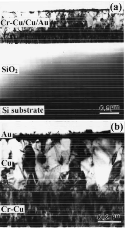
The solder materials which IBM used to joint these two substrates are usually 95Pb5Sn or 97Pb3Sn. A schematic diagram of cross-section of the joint is shown in Fig. 2.4. The on-chip solder bump can be deposited by evaporation and patterned by lift-off or by selective electroplating. It usually has a melting point over 300°C. The UBM on the chip surface is usually a tri-layer thin film of Cr/Cu/Au and the TSM on the ceramic surface is typically Ni/Au. The substrate usually consists of three layers: adhesion and/or barrier layer, wetting layer, and oxidation barrier layer. For example of Cr/Cu/Au, Cr layer is selected to be adhesion layer to form a strong bond with Al pad and to improve the adhesion of Cu to SiO2 chip surface. Moreover, IBM has further developed the phased-in Cu–Cr microstructure to improve the adhesion between Cu and Cr, as shown in Fig. 2.5. Since Cu and Cr are immiscible, their grains form an interlocking microstructure which improves the adhesion between them when they are co-deposited.
A Cu layer is selected to be wetting layer to form a strong bond with the Al pad and with the passivation layer. The Cu wetting layer is made to improve interconnection for its reaction with Sn to form intermetallic compound(s) during packaging. Finally, the oxidation barrier layer is made of Au, which protects the wetting layer from oxidation and corrosion.
Fig. 2.1 The first three levels of electronics packaging. [11]
Fig. 2.2 (a) flip chip, (b) wire bonding, and (c) tap bonding. [12]
Fig. 2.3 Various flip chip technologies. [11]
Fig. 2.4 IBM’s C4 (Controlled Collapse Chip Connection) technology. [11]
Fig. 2.5 Cross-sectional transmission electron microscopy images. (a) The Cr–Cu/Cu/Au multilayer on oxidized Si wafer; (b) the enlarged image of the multilayer in (a). [14]
2.2 Phase diagram
Knowledge of intermetallic(s) phase evolution in the solder joints from phase diagram is important to improve the reliability of the solder joints, because the formation of intermetallic compound(s) at the solder–substrate interface can provide a good wetting and a good metallurgical bonding, and it produces distinct improvement in mechanical properties of joints if the growth of intermetallics is not excessive.
Generally, binary phase diagram is useful to understand the phase formation in the interaction of two solid parent phases. For example, Fig. 2.6 shows a Cu–Sn binary phase diagram [15], in which the intermetallic compounds ε-Cu3Sn and η-Cu6Sn5 form below temperature 350°C in addition to solid solutions (Cu) and (Sn). If two planar plates of pure Cu and pure Sn are welded together and annealed at the temperature 190°C for enough annealing time, both of the two intermetallic phases Cu3Sn and Cu6Sn5 are expected to appear. The phase sequence in such the diffusion couple is the same as the phase sequence in the temperature–composition diagram (see Fig. 2.6), i.e., Cu/(Cu)/Cu3Sn/Cu6Sn5/(Sn)/Sn. However, a typical solder reaction involves at least three elements: two in solder alloy and one in the conducting substrate, such as the case of PbSn/Cu. In such the case of solder joints, the binary phase diagrams cannot provide sufficient information on the phase evolution in solder–substrate reactions because they do not bear any information on the relative stabilities of its phases in the presence of a third element in the multicomponent system. For example [16-17], only Cu6Sn5 formed at the interface when Cu was soldered with 63Sn37Pb at 283°C. But Cu3Sn formed at the interface instead of Cu6Sn5 when Cu was soldered with 95Pb5Sn at 400°C. However, if Cu was pretinned with the 95Pb5Sn solder and then aged at 170°C, only Cu6Sn5 appeared between Cu and solder. Since both of Cu3Sn and Cu6Sn5 were stable at these temperatures according to the Cu–Sn phase diagram, it is difficult to explain these experimental results
in solder–substrate reactions from binary phase diagrams. Although Pb did not involve in the interfacial reaction to form any intermetallic compound in PbSn/Cu reactions, the addition of Pb decreased the activity of Sn and then affected the Cu–Sn reactions.
Therefore, we need the corresponding ternary phase diagram, Pb–Sn–Cu phase diagram, in order to understand the phase evolution of intermetallic compound(s) in solder–substrate reactions.
Interdiffusion in a ternary system is much more complicated than in a binary system.
Experimental ternary phase diagrams for most of the solder joint systems are even unavailable. Even if one joint system has been experimentally studied, the isotherm sections of the diagram at the interest temperature have rarely been measured. With the rapid development of computer technology, the CALPHAD (Calculation of Phase Diagram) technique has been developed to investigate the phase equilibria of ternary systems or higher order systems [18]. In this method, thermodynamic properties of a system are analyzed by using thermodynamic models for the Gibbs free energy of individual phases. With selected model, parameters of thermodynamics in this system can be defined from experimental data or estimated. Once the Gibbs free energy functions of all the phases in the system have been obtained, in principle, any kind of phase diagrams and thermodynamic properties of interest may be calculated. Compared the composition of calculated diagram at the temperature of interest with the experimental data, we can revise the model or parameters for verification of the diagram. The detail application and description of CALPHAD may refer to reference of [18-22], if reader needed further understanding. In this study, studied phase diagram by CALPHAD was used to discuss the interfacial evolution in soldering reactions. With the help of CALPHAD technique, the phase diagrams can be available in a wide temperature range including the temperatures of interest in technology or industry. Since a solder joint involves initially a
solid–liquid reaction between molten solder and metal substrate, followed by solidification and a solid state aging during device operation or storage, calculation of phase diagram technique is necessary to improve the understanding of solder joints.
Although the complete phase equilibrium is never reached in interconnection applications, the local equilibrium at phase interfaces was assumed to be achieved in a bulk diffusion couple in a short time [23]. Thus, it assumed that after reactions every two neighboring phases (planar layers) are in equilibrium, which is represented either by a two-phase equilibrium region in a binary phase diagram or by a tie-line in isothermal section of a ternary phase diagram at the interest temperature [24]. Since the assumption of local equilibrium in bulk diffusion couple can be applied to the reactions between molten solder and metal substrate [25], the ternary phase diagrams can indeed provide useful information about the solder–substrate reactions, such as the information from diffusion path presented in next section.
Fig. 2.6 The Cu–Sn phase diagram. [15]
2.3 Diffusion path
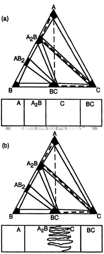
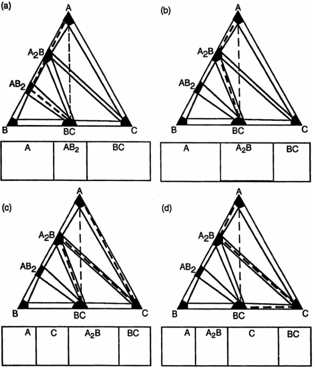
Due to this local thermodynamic requirement, neighboring phases in a reacting diffusion couple must be connected by a tie-line in the isotherm section of a ternary phase diagram. Therefore, the interfacial reactions in a ternary system can be graphically described by a diffusion path that is composed of several two-phase tie-lines in the ternary phase diagram. Since diffusion and reactions in a ternary diffusion couple can preceed through many potential diffusion paths, three rules are developed to exclude many of the potential paths [26-31].
The first rule is that the diffusion paths have to be consistent with the local equilibrium. Four assumed diffusion paths with simple layer structure for a diffusion couple, A/BC, are illustrated in Fig. 2.7. Except for the diffusion path in Fig. 2.7(a), diffusion paths in Figs. 2.7(b)–(d) are consistent with the local thermodynamic requirement. Diffusion path in Fig. 2.7(a) is not consistent with the local thermodynamic requirement because of the A phase and AB2 are not at thermodynamic equilibrium from the isotherm section of the A–B–C phase diagram but AB2 is formed next to A in the diffusion couple. If the diffusion path in Fig. 2.7(a) does exist, there is a driving force for the A2B to nucleate at the A/AB2 interface and then the phase sequence in the diffusion couple would be A/A2B/AB2/BC.
The second rule is that the diffusion path must fulfill the mass conservation law: no material can be lost or created during reactions, which forces the diffusion path to cross the straight line joining the terminal compositions (so-called mass balance line) at least once [26]. This rule of mass conservation must be strictly applied to any ternary diffusion couple in a closed system, or the analysis is wrong or there is material lost during reactions. According to mass balance arguments, the diffusion paths in Figs. 2.7(c) and (d) are consistent with this rule; however, the diffusion path in Fig. 2.7(b) seems to violate
this rule due to the whole diffusion path lies on one side of the line connection A and BC.
In fact, the diffusion path in Fig. 2.7(b) acts in accordance with the mass balance consideration if the composition change of BC can be exaggerated for the sake of readability. Fig. 2.8 shows the case of PbSn/Cu soldering reactions. Theoretically, at the local equilibrium solubility, the intermetallic compound starts to form at the solder–substrate interface although metastable supersaturation usually occurs in this part of solder. For the solder of composition A (see Fig. 2.8), with the growth of intermetallic compound, more and more Sn atoms are taken away from the solder and then the solder composition at the interfacial region moves along the liquidus line towards the Pb-rich side as indicated by arrow a. According to the exaggerated illustration at composition A, the straight line connecting the composition A and Cu cross the diffusion path A (thick dashed line). Therefore, the diffusion path in Fig. 2.7(b) complies with the rule of mass balance.
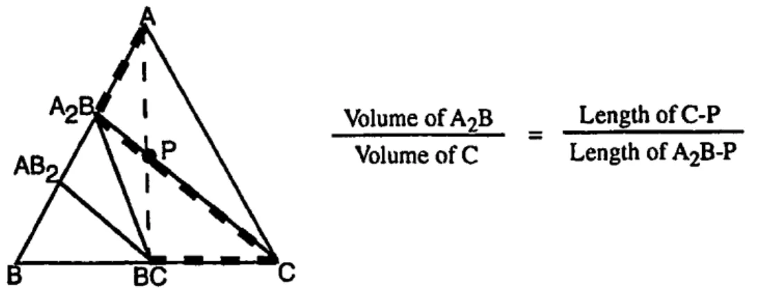
In certain instances, the consideration of mass conservation may also be applied to speculate the relative amount of the reaction products. When all the phases involved in an isotherm exhibit a limited range of homogeneity, the reaction product can be applied by lever rule. As illustrated in Fig. 2.9, the point P is the crossing point of the line connecting the reactants A and BC and the line connecting the products C and A2B. At any instant during the reaction, the ratio of A2B and C must be consistent with the rule depicted in Fig. 2.9.
The third rule is that the diffusion path must obey the kinetic consideration concerning the diffusional driving force for elements. This rule has been described by van Loo et al. [28] as follows: In a diffusion couple the elements only intrinsically diffusion into a direction in which their own chemical potentials are lowed and the upwards-diffusion is, in fact, caused by the mobility of the other components. In a stable
binary solution, the sign of the chemical potential gradient is always the same as that of the concentration gradient. However, higher component concentration does not always mean higher component chemical potential in ternary and higher-order systems.
Moreover, in ternary systems with compounds of small ranges of homogeneity, a very small change in composition can cause great changes in the component chemical potentials. This is due to the fact that compounds with small ranges of homogeneity usually have high values for the thermodynamic factor. Therefore, in such compounds, the driving force for diffusion may appear to be small in terms of the composition gradient, but large in terms of the chemical potential gradient. In order to rationalize the diffusion behavior in ternary systems in the better measure of chemical potential, we need the stability diagrams, which show the chemical potential of one of the components as a function of composition at certain temperature and pressure.
The determination of stability diagrams for an isotherm may become complicated if one or more phases exhibit appreciable ranges of homogeneity. Fortunately, with the development of computer calculation in phase diagram, the stability diagram can be calculated readily of the corresponding ternary phase diagram has been computer-modeled properly. Compared to the conventional isotherm mapping the phase relationships in “composition space”, the stability diagram maps the phase relationships in “chemical potential space”. That is much more useful for rationalizing diffusion behavior in diffusion couples. For example, both of diffusion paths in Figs. 2.7(c) and (d) satisfy the thermodynamics and mass-balance requirements for the diffusion couple A/BC. But only diffusion path in Fig. 2.7(d) is allowed by kinetics consideration. For the diffusion and reaction in Fig. 2.7(d), in order for the growth of A2B phase, A atoms have to diffuse through the A2B phase and B atoms have to diffuse through the C phase. The diffusion path corresponding to diffusion couple in Fig. 2.7(d) has been imposed as the
thick dashed line on the stability diagram of Figs. 2.10(b) and (c) for A and B atoms, respectively. It is clear that this diffusion path satisfies the kinetic rule because both A and B diffuse down its own chemical potential gradient. However, for diffusion and reaction in Fig. 2.7(c), C atoms have to diffuse through the A2B phase in order to grow C phase and A atoms have to diffuse through the C and A2B phase in order to grow A2B phase.
The diffusion path corresponding to diffusion couple in Fig. 2.7(c) has been imposed as the thin dashed line on the stability diagram of Fig. 2.10(a) and (b) for C and A atom, respectively. It is clear that A atom does diffuse down its own chemical potential gradient but C atom must diffuse up its own chemical potential, which is not allowed by the kinetic rule. Therefore, the diffusion path in Fig. 2.7(c) is kinetically impossible.
The hypothetical isotherm in Fig. 2.7 is helpful to illustrate that the rules governing the diffusion paths in ternary diffusion couples originate from the thermodynamics, mass-balance, and kinetics considerations. For applications of experimental results, diffusion path can be plotted from the corresponding interfacial microstructure and these considerations are helpful for use of diffusion path for rationalizing interfacial phase evolution. For example, Sunwoo et al. [17] immersed Cu plates into the molten 63Sn37Pb solder bath at 283°C for 2–3 min and then quenched the bath into iced water.
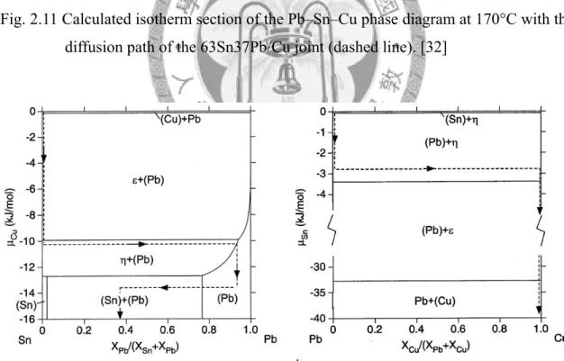
After quenching, the sample was aged at 170°C for up to 84 days. Only the layer of Cu6Sn5 was observed in the as-soldered sample. After aging for several days, a thinner layer of Cu3Sn appeared between Cu and the coarsened Cu6Sn5 and a layer of Pb-rich phase was built up between the solder and Cu6Sn5. According to the phase sequence of interfacial microstructure, the corresponding diffusion path at 170°C is solder→Pb-rich solid solution→η-Cu6Sn5→ε-Cu3Sn→(Cu), as represented by the dashed line in Fig.
2.11 [32]. With the information of calculated stability diagram in Fig. 2.12, it not only indicates that this path satisfies the kinetic rule but also shows the driving force for both
of Sn and Cu to diffuse through the multilayered microstructure, solder/(Pb)/Cu6Sn5/Cu3Sn/(Cu). Zeng et al. [32] immersed Cu wires into the molten 51.3Sn48.7Bi solder bath at 235°C for 95 hand then the Cu wires were transferred into another solder bath of 80.4Bi19.6Sn at the same temperature for 300 s. After the first treatment, the intermetallic layers of Cu6Sn5 and Cu3Sn were observed at interface, as shown in Fig. 2.13(a). However, Fig. 2.13(b) shown all the previously formed Cu6Sn5 at the interface transformed into the Cu3Sn after the second treatment. According to the calculated isotherm in Fig. 2.14, the interfacial microstructure in the first treatment can be rationalized by diffusion path. And with the help of the phase diagram in Fig. 2.14, in the second treatment, the compound phase that can be in local equilibrium with the molten solder of higher Bi content is no longer η-Cu6Sn5 but ε-Cu3Sn and thus the previously formed η-Cu6Sn5 phase is not stable. Stability diagram (see Fig. 2.15) indicates that at 235◦C the minimum chemical potential of Sn (μSn) at the L/η interface is ﹣3.37 kJ/mol, while the value of μSn in the second solder bath is ﹣4.63 kJ/mol (see point b). Therefore, after the second treatment the Sn atoms in the previously formed η-Cu6Sn5 phase has a driving force of at least ﹣1.26 kJ/mol to move into the molten solder, resulting in the transformation of η-Cu6Sn5 into ε-Cu3Sn.
In the beginning of this section, the important difference between binary and ternary systems was already mentioned. The extra degree of freedom in a ternary system allows the occurrence of different types of structures within the diffusion zone. Two types of reaction product morphologies, simple layered and aggregate are known to occur in ternary diffusion couples [31, 33-34]. The simple layered structure and the aggregate structure are illustrated schematically in Figs. 2.16(a) and (b) respectively.
The diffusion paths plotted on the isotherms of Figs. 2.16(a) and (b) look similar but they correspond to different microstructures. In Fig. 2.16(a), the interface between A2B
and C is planar, and the diffusion path in the A2B–C region coincides with one of the tie lines in the A2B–C two phase region of the isotherm. Whereas, in Fig. 2.16(b), the interface between A2B and C is non-planar, and the diffusion path in the A2B–C region crosses several tie lines in the A2B–C two phase region of the isotherm.
Due to the limited supply of constituents from solder or substrate in solder joints, the availability or mass supply of the constituents that are involved in the interfacial reactions plays a very important role in the phase evolution after the formation of the first intermetallic phase. Since the diffusion path is defined as the set of the average compositions measured in a plane parallel to the original interface going from one starting material to the other, the application of diffusion path to interfacial reactions in solder joints should be considered carefully. In order to demonstrate the diffusion path validly, in this study we perform the experiment of soldering reactions between a large amount of solder and substrate in purpose for staying the composition of solder nearly constant during reaction.
Fig. 2.7 Four assumed diffusion paths with the simple layered structure for diffusion couple A/BC. The diffusion paths are traced as the thick dashed lines on the isotherms. Not all diffusion paths illustrated here are allowed (see section 2.3).
Diffusion path in (a) is not consistent with the thermodynamic requirement.
Diffusion path in (d) is not in accordance with kinetics consideration.
Diffusion paths in (b) and (d) are consistent with the thermodynamics, mass-balance, and kinetics considerations. [30]
Fig. 2.8 Calculated isotherm section of the Pb–Sn–Cu phase diagram at 350°C together with diffusion paths A (thick dashed line) and B (thin dashed line). The dotted-dashed lines are connection lines between Cu and the original solder compositions. Arrow a and b indicate the composition changes (exaggerated for the sake of readability) of the two solders due to the intermetallic formation.
Phase notation: η-Cu6Sn5, ε-Cu3Sn, L-liquid. [32]
Fig. 2.9 Lever rule for the two new phases A2B and C formed between diffusion couple end members A and BC. [30]
Fig. 2.10 Stability diagrams for the phase diagram shown in Figs. 2.7(c) and (d). [30]
Fig. 2.11 Calculated isotherm section of the Pb–Sn–Cu phase diagram at 170°C with the diffusion path of the 63Sn37Pb/Cu joint (dashed line). [32]
Fig. 2.12 Phase stability diagrams of the Pb–Sn–Cu system at 170°C in the form of chemical potential of (a) Cu, and (b) Sn, as a function of the atom ratio of the other elements. A schematic reaction path for the 63Sn37Pb/Cu joint has been imposed as the dashed line on the diagrams. [32]
Fig. 2.13 SEM micrographs of the Sn–Bi solder/Cu interfaces. (a) Treatment I: solder bath composition 51.3Sn48.7Bi, 235°C, 95 h. (b) Treatment II: solder bath composition: 80.4Bi19.6Sn, 235°C, 300 s. The η-Cu6Sn5 phase formed by Treatment I has transformed into ε-Cu3Sn in Treatment II. [32]
Fig. 2.14 Calculated isotherm section of the Pb–Sn–Cu phase diagram at 235°C. [32]
Fig. 2.15 Phase stability diagram of the Cu–Sn–Bi system at 235°C in the form of chemical potential of Sn as a function of the atom ratio of the other elements.
Points a and b denote the value in the first and second solder bath, respectively.
[32]
Fig. 2.16 Schematic illustrations for structure with its diffusion path. (a) the simple layered structure, (b) the aggregated structure. [30]
2.4 Spalling phenomenon
In electronic solder joints, the detachment of intermetallic compound(s) form the solder–substrate interface has been an important issue due to the reliability concern of electronic devices. Consequently, knowledge of spalling phenomenon in solder–substrate reaction during soldering or aging is necessary in order to improve the reliability of electronic products.
In solder joints research, spalling was originally used to describe the granular detachment of the intermetallic compounds, the reaction product, from the interface during the reaction. A typical experimental observation is the spalling of Cu6Sn5 during soldering reaction between eutectic PbSn solder and Cu/Cu–Cr metallization, as shown in Fig. 2.17 [14]. It had been found that the spalling of Cu6Sn5 grains was caused by the exhaustion of the Cu film, which had a good wetting with Cu6Sn5. Therefore, the dewetting contact between Cu6Sn5 and the remaining Cu–Cr layer, and the subsequent conservative ripening growth of Cu6Sn5 lead to the spalling of Cu6Sn5 as individual grains into the molten solder. Similar spalling phenomenon of eutectic SnPb soldered on Ni/Ti thin films was also reported [35]. Fig. 2.18 represents the evolution of the spalling process for eutectic SnPb on Cu/Cr or Ni/Ti thin films; (a) initial stage of ripening growth, (b) final stage of spalling of the compound grains into the molten solder.
Compared to the regular spalling mentioned above, another type of spalling was recently of considerable attention. The entire intermetallic compound layer, reaction product, detached itself from the solder–substrate interface on an unusually large scale during reaction before disintegration into individual intermetallic grains. Such a phenomenon was regarded as massive spalling [9] which was observed in several solder–substrate systems, including SnAgCu reacted on Ni substrate [2-4], SnZn on Cu [5-6], high-Pb PbSn on Cu [7] and high-Pb PbSn on Ni [8]. The massive spalling differs
from the regular spalling in two ways: the apparent difference in the scale of spalling and the fact that the massive spalling can occur even when the wettable layer is intact.
Recently, a unified thermodynamic argument is proposed to rationalize this massive spalling phenomenon [9]. According to this model, two necessary conditions must be met for the massive spalling to occur. The first condition is that at least one of the reactive constituents of the solder must be presented in a limited amount, and the second is that the joint reaction must be very sensitive to the concentrations of the constituent.
With the growth of initial intermetallic compound, more and more constituent atoms are extracted out of the solder and incorporated into the intermetallic compound. As the concentration of this constituent near the interface dropped below the level where the initial intermetallic compound was no longer in equilibrium with the molten solder, the initial intermetallic compound at the interface became a non-equilibrium phase, and then massive spalling of the initial intermetallic compound occurred. The thermodynamic argument is applied to the four following cases to explain the massive spalling phenomenon.
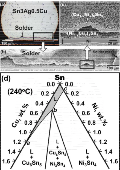
In the case of SnAgCu/Ni soldering reaction [3-4], Sn3Ag0.5Cu solder ball of 760 μm was soldered on Au/Ni substrate with a 600-μm-diam opening. During soldering, the peak temperature was 235°C and the time during the solder was molten was 5 min.
As shown in Fig. 2.19, the outer (Cu1-xNix)6Sn5 layer had detached itself from the interface, and the (Ni1-yCuy)3Sn4 was still attached to the Ni substrate. The gap between these two layers was originally occupied by the solder, but the solder there was etched away during sample preparation. It is clear from Figs. 2.19(a) and (c) that the massive spalling occurred across the entire joint. The Sn–Cu–Ni isotherm (see Fig. 2.19 (d)) shows that solders with different Cu concentration are in equilibrium with different phases. When the Cu concentration is high (between a and b), the molten solder is in
equilibrium with (Cu1-xNix)6Sn5, and when the Cu concentration is low (between b and c), the molten solder is in equilibrium with (Ni1-yCuy)3Sn4. At point b, the molten solder, (Cu1-xNix)6Sn5, and (Ni1-yCuy)3Sn4 are in three-phase equilibrium. As (Cu1-xNix)6Sn5 or (Ni1-yCuy)3Sn4 grew thicker during reaction, more and more Cu atoms in the solder were extracted out of the solder and became incorporated into (Cu1-xNix)6Sn5 or (Ni1-yCuy)3Sn4. Consequently, the Cu concentration of solder will markedly decrease with the growth of the reaction product(s) and result in the shifting of phase equilibrium at the interface from initial (Cu1-xNix)6Sn5+L to (Ni1-yCuy)3Sn4+L. Therefore, there will be a driving force for (Cu1-xNix)6Sn5 to leave the interface in order to form a more stable (Ni1-yCuy)3Sn4 and then the massive spalling of (Cu1-xNix)6Sn5 occurred.
In the case of high-Pb PbSn/Cu aging reaction [7], the Cu3Sn formed during soldered to form spherical bump and adhered well to the interface after as-soldered.
Massive spalling of Cu3Sn was not observed after 200 h of solid-state aging at 170°C, and only after 500 h of aging could massive spalling of Cu3Sn be observed. Fig. 2.20(a) shows the microstructure of massive spalling after aging at 170°C for 1000 h. Jang et al.
pointed out that spalling occurred because Sn near the interface had been consumed locally, and the diffusion of Sn in the solder was so slow that those Sn atoms far away from the interface could not diffuse back to the interface fast enough to keep the Sn concentration up. According to the Pb–Sn–Cu isotherm at 170°C shown in Fig. 2.20(b), the local equilibrium at the interface changes from the Cu6Sn5+(Pb) two-phase field, to the Cu3Sn+(Pb) two-phase field, then to the (Cu)+(Pb) two-phase field with decreasing the Sn concentration. Therefore, massive spalling phenomenon was again caused by the depletion of the most reactive constituent (Sn in this case of high-Pb/Cu joint reaction) in the solder, although here the depletion occurred only locally near the interface.
In the case of high-Pb PbSn/Ni soldering reaction [8], the massive spalling of
Ni3Sn4 was observed after soldering at 350°C for 90 min, as shown in Fig. 2.21(a). Fig.
2.21(b) shows the Pb–Sn–Ni isotherm at 250°C which was calculated by Ghosh [36].
Although the Pb–Sn–Ni isotherm at 350°C is not available, the isotherm at 250°C should give a reasonable approximation of the geometry of the phase relationships. Fig.
2.21(b) shows that the equilibrium phase with (Pb) changes from Ni3Sn4 to Ni3Sn4, and then to Ni3Sn with decreasing the Sn concentration. With the growth of Ni3Sn4, more and more Sn atoms were extracted out of the solder. Eventually, the Sn concentration dropped to a level where the Ni3Sn4 was no longer stable at the interface, and then the massive spalling of Ni3Sn4 occurred.
In the case of SnZn/Cu soldering reaction [5], 99Sn1Zn solder ball of 10 mg was soldered on pure Cu at 250°C for 2 min. As shown in Fig. 2.22(a), the outer CuZn layer had detached itself from the interface, and the Cu6Sn5 was still attached to the Cu substrate. The gap between these two layers was originally occupied by the solder, but the solder there was etched away during sample preparation. According to intermetallic thickness calculation, the Zn concentration in the solder dropped from 1 wt.% to 0.64 wt.% after 2 min of reaction. Sn-rich corner of the Sn–Zn–Cu isotherm (see Fig. 2.22 (b)) shows that solders with different Zn concentration are in equilibrium with different phases. When the Zn concentration was 1 wt.%, the (Sn)+Cu6Sn5+CuZn three-phase field dominated, and both Cu6Sn5 and CuZn formed. After reaction time of 2 min, the equilibrium phase field changed from (Sn)+Cu6Sn5+CuZn three-phase field to (Sn)+Cu6Sn5 two-phase field. As a result, CuZn was no longer an equilibrium phase at the interface and it spalled into the solder, as shown in Fig. 2.22(a).d
Since the argument can successfully rationalize the massive spalling phenomenon in above three cases, the concentration of the reactive constituent in the solder was always difficult to measure and could only be estimated. Therefore, this model had been
further verified experimentally that the driving force for massive spalling is thermodynamic [37]. Carefully designed experiments of swapping solder were carried out. The original Sn0.6Cu solder reacted with pure Ni to form (Cu,Sn)6Sn5 at the interface was removed and replace with Sn0.3Cu solder. Fig. 2.23 shows the massive spalling of (Cu,Sn)6Sn5 occurred in order to accommodate the stable (Ni,Cu)3Sn4
because the change of composition of the most reactive constituent in the solder resulted in the change of the stable phase in equilibrium with the solder. It is concluded that the driving force for massive spalling is indeed purely thermodynamic in nature and the massive spalling phenomenon should be regarded as a process through which the interface responds to the shifting of the equilibrium phase. The massive spalling occurs because the original reaction product at the interface is no longer in local thermodynamic equilibrium with the solder and this intermetallic spalls away to make room for the subsequent nucleation and growth of the new equilibrium phase.
However, Fig. 2.24 shows massive spalling had been also observed during Sn0.7Zn/Cu soldering reaction in which the interfacial thermodynamic condition was static [6]. The average Zn concentration in the Sn0.7Zn/Cu soldering reaction could remain nearly constant during reactions due to a large solder volume was used purposely.
Since the massive spalling was observed without shifting of equilibrium phase, the occurrence of massive spalling in Sn0.7Zn/Cu soldering reaction must be explained by another reason other than the thermodynamic argument proposed by Yang et al. [9].
Fig. 2.17 Cross-sectional SEM image of eutectic PbSn soldered on the Cu/Cu–Cr/Au UBM for samples soldered at 200◦C for 600 s, showing the ripening and spalling of intermetallic compound Cu6Sn5. [14]
Fig. 2.18 Schematic diagrams depicting the phenomena of (a) ripening among the scallop-type IMC, (b) spalling of the spheroid-type IMC. [10]
Fig. 2.19 Micrograph showing the massive spalling in a solder joint of Sn3Ag0.5Cu soldered on Au/Ni after soldering time of 5 min at peak temperature of 235°C.
(a) The entire cross-sectional view of solder joint. (b) Zoom-in micrograph of (a). (c) Zoom-in of (b) and the outer (Cu1-xNix)6Sn5 layer had detached itself from the interface, and the (Ni1-yCuy)3Sn4 was still attached to the Ni substrate.
(d) Sn-rich corner of the Sn–Cu–Ni isotherm at 240°C (Ref. [4]). [9]
Fig. 2.20 (a) Micrograph showing the massive spalling in a 95Pb5Sn/Cu solder joint after aging at 170°C for 1000 h observed by Jang et al. [7]. The completely detached layer was Cu3Sn. (b) The Pb–Sn–Cu isotherm at 170°C. The phase relations in this isotherm are from the study of Tu and Zeng [10].
Fig. 2.21 (a) Micrograph showing the massive spalling in a 95Pb5Sn/Ni solder joint after soldering at 350°C for 90 min observed by Wang and Chen [8]. The completely detached layer was (Ni1-yCuy)3Sn4. (b) The Pb–Sn–Ni isotherm at 250°C. The phase relations in this isotherm are from the study of Ghosh [36].
Fig. 2.22 (a) Micrograph showing the massive spalling in a 99Sn1Zn/Cu solder joint after soldering at 250°C for 2 min observed by Yang et al.[5]. The completely detached layer was CuZn. (b) Sn-rich corner of the Sn–Zn–Cu isotherm at 250°C (Ref. [38]).
Fig. 2.23 Specimens with (Cu,Sn)6Sn5/Ni structure reacted with Sn0.3Cu solder at 250°C for (a) 1, (b) 2, (c) 3, and (d) 10 min. Early stage of spelled (Cu,Sn)6Sn5 is visible in (a), and complete spalling can be seen in (b) and (c).
[37]
Fig. 2.24 Micrograph showing the Sn0.7Zn/Cu interface after reaction at 250°C for 10 min. The entire CuZn layer had massively spalled into the solder. [6]
2.5 Grain boundaries penetration
In this study of chapter 4.2, the phenomenon of grain boundaries (GBs) penetration was observed in high-Pb/Ni soldering reactions. Fig. 2.25 shows the molten high-Pb phase penetrated into Ni substrate along grain boundaries in high-Pb/Ni soldering reactions at 400°C for 240 min. Although the phenomenon of GBs penetration is not the aimed purpose of the experiment, understanding of GBs penetration is helpful to discuss the microstructure evolution of high-Pb/Ni soldering reaction. Moreover, compared to the extensive studies of solder on Cu, it is timely to get more understanding of the soldering behavior of Ni substrate due to Ni-based UBM has been notable for good wettability, good diffusion barrier ability, and slow reaction rate with Sn. Therefore, the introduction of the GBs penetration is reviewed here.
Contact of solid metal with a liquid one may bring on rapid penetration of a liquid phase along the GBs of a polycrystalline solid [39]. Typical experimental observation (Figs. 2.26–2.30) had been found in numerous solid-liquid metal pairs even if the liquid is over-saturated by the constituents of the solid, such as Ni–Pb [40-41], Ni–Bi [42], Cu–Bi [43-44], Al–In [44] and, Al–Ga [45-46]. Generally, the condition of mechanical equilibrium at the top of the groove is satisfied (Fig. 2.31):
( )
sl gb
2 cos θ / 2γ =γ
(2.1) where
γ
gb andγ
sl are the energies of the grain boundary and of the solid/liquid interface, respectively. It should be noted that the relation of equation 2.1 is only valid while both ofγ
gb andγ
sl are independent of the crystallographic orientation.The GBs grooves are characterized by the dihedral angel, θ. If the dihedral angle is always obtuse and close to 2 rad and the grooving rate is usually a few micrometers per hour, the grooves are referred to thermal grooves which is known as the Mullins type
GBs grooving [47]. By contrast, the dihedral angle is always acute and the grooving rate is ten to hundreds of micrometers per hour, the grooves are referred to liquid grooves known as the rapid GBs penetration. The main physical differences between thermal grooves and liquid grooves are illustrated in Fig. 2.32.
The liquid–solid interface in this case of liquid grooves has relatively low interfacial energy in comparison with the typical energy of a high angle grain boundary [48]. Hence, the dihedral angle at the top of the groove is always acute, in contrast to the case of thermal grooves, and may even reach its limit value of zero, which corresponds to complete wetting. Therefore, the classical theory of GBs grooving used by Mullins [47] is inapplicable to discuss the liquid grooves due to the participation of grain boundary diffusion in the material transport is negligible in classical theory.
Vogel and Ratke [44] first pointed out that the formation of the liquid groove clearly differs from that characteristic of a Mullins type groove by using the Al-In system as an example. The In diffusion along the Al grain boundaries caused by the liquid grooves was found and resulted in the liquid solution near the top of the groove is depleted in In and enriched in Al. In some cases the liquid grooving is also based on the assumption of a highly faceted solid/liquid interface [40]. In such circumstances the dynamic process would be governed not only by diffusion access of atoms to the interface but also essentially by the rate of their assimilation by the latter.
Fig. 2.25 Grain boundaries (GBs) penetration of Ni substrate by molten high-Pb in high-Pb/Ni soldering reaction at 400°C for 240 min.
Fig. 2.26 Ni polycrystals exposed to the Pb melt at 740°C for 210 min. [41]
Fig. 2.27 Intergranular Bi-rich film on a polycrystalline Ni specimen after 16 h of exposure at 700°C. [42]
Fig. 2.28 Cu polycrystals exposed to the melt Cu-rich liquid Bi (89Bi11Cu) at 600°C for 4 h. [43]
Fig. 2. 29 Al polycrystals exposed to the melt In–Al alloy (89Bi11Cu) at 550°C for 17.5 h. [44]
Fig. 2.30 Microradiographs showing liquid Ga penetration along an Al bicrystal grain boundary. The temperature of the Al bicrystal is controlled in order to trigger the grain boundary penetration process (Tm=29.8°C for Ga). [46]
Fig. 2.31 Cross section of an equilibrium groove.
Fig. 2.32 (a) Thermal grooves (TG) and (b) liquid grooves (LG).
Chapter 3 Experimental procedures
3.1 Preparation of substrates
Pure Cu strip and pure Ni strip were used to be substrate in high-Pb/Cu and high-Pb/Ni soldering reactions, respectively. Strips of dimension 25 mm × 10 mm × 4 mm were cut from a pure grade Cu (99.9%) and Ni (99.99%) plates. Each substrate was mirror-polished on both faces. To remove the oxide layer on the surface of substrate, the Cu substrates were etched in 50% deionized water solution of HNO3 and the Ni substrates were etched in 5% deionized water solution of HCl, followed by cleaning in ethanol and dried in air.
3.2 Preparation of solder alloys
High-Pb solder alloys (PbxSn) with different Sn concentrations (x=0.5, 1, 3, 5 wt%) were prepared in this study and elemental Pb (Alfa AESAR, Pb powder, 99.999%) and Sn(Alfa AESAR, Sn granules, 99.99%)were used for alloy preparation. Proper amounts of Pb and Sn were weighed on an electronic balance (SCALTEC, accuracy of 0.0001 g) and encapsulated in a quartz tube of 10-2 torr vacuum. The sample tubes were placed in a furnace (Lindberg, Blue M, U.S.A.) at 600°C for complete mixing and then quenched in iced water. The quenched tubes were further annealed in a furnace at 300°C for 2 weeks for alloy homogenization.
3.3 high-Pb/Cu soldering reactions
Each solder bath was formed by placing 12 g of solder alloy into a quartz tube of 10 mm inside diameter and then was heated to 350°C by a homemade furnace equipped with heater, thermal couple, PID controller (RKC CB100FK07), and solid–state relay
99.5Pb0.5Sn, 99Pb1Sn, 97Pb3Sn, and 95Pb5Sn, were investigated. While the solder bath was steady at reaction temperature, the Cu substrate fluxed with commercial rosin mildly activated flux was immersed in the molten solder. The reaction time ranged from 1 min to 20 min. Besides, for extreme demonstration, the reaction time of 95Pb5Sn/Cu was prolonged to 600 min and the reaction time of 99.5Pb0.5Sn/Cu was shortened to 10 s.
After reaction, the tube along with the solder was immediately quenched in iced water.
3.4 high-Pb/Ni soldering reactions
In high-Pb/Ni soldering reaction, the reaction time ranged from 2 min to 240 min because the growth rate of Ni–Sn intermetallics is much slower than Cu–Sn intermetallics.
In order to coordinate with the literature diagram data for accurate thermodynamic analysis, the reaction temperature was set to be 400°C. Moreover, the solder alloy of three different compositions, 99Pb1Sn, 97Pb3Sn, and 95Pb5Sn, were investigated. The whole reaction process in high-Pb/Ni soldering reaction was similar with high-Pb/Cu soldering reaction, such as the volume of reaction solder (12 g).
3.5 Metallographic and analysis
The quenched samples were further sliced for solder–substrate interfacial examination. Samples for cross-sectional examination were prepared by two techniques:
(I) conventional metallographic grinding and polishing and (II) ion-milling cross-sectional polishing (E-3500; Hitachi, Tokyo, Japan). In the treatment I, the reagent, four parts nitric acid, four parts glacial acetic acid and 16 parts deionized water, was used for metallographic etching. But in the treatment II, no chemical reagent of surface etching was used. The ion-milling polishing has the benefit of less sample damage but is more time consuming. The demonstration of ion-milling polishing for cross-sectional examination is shown in Fig. 3.2. A scanning electron microscope (SEM; S3000-N;
HITACHI, Japan) equipped with a backscattering electron detector was used to inspect and analyze the interfacial microstructure. The compositions of the phases were determined by a state-of-the-art field-emission electron probe micro-analyzer (FE-EPMA;
JXA-8500F; JEOL, Japan) with average value of measurements from five different regions in the intermetallic layer. The thicknesses of intermetallic layer used for residual concentration calculation were the average thickness evaluated by dividing the area of intermetallic layer by the length of interface. The area and length are measured through digital SEM pictures and imaging processing software (Optimas, U.S.).
Fig. 3.1 Illustrated homemade equipment for soldering reaction.
Fig. 3.2 The demonstration of ion-milling polishing for cross-sectional examination.
![Fig. 2.6 The Cu–Sn phase diagram. [15]](https://thumb-ap.123doks.com/thumbv2/9libinfo/9604888.631017/26.892.144.742.389.832/fig-the-cu-sn-phase-diagram.webp)
![Fig. 2.10 Stability diagrams for the phase diagram shown in Figs. 2.7(c) and (d). [30]](https://thumb-ap.123doks.com/thumbv2/9libinfo/9604888.631017/35.892.131.759.160.1067/fig-stability-diagrams-phase-diagram-shown-figs-c.webp)
![Fig. 2.14 Calculated isotherm section of the Pb–Sn–Cu phase diagram at 235°C. [32]](https://thumb-ap.123doks.com/thumbv2/9libinfo/9604888.631017/38.892.245.659.127.503/fig-calculated-isotherm-section-pb-sn-phase-diagram.webp)