應用雙耦合線之雙頻結構
邱順興 曾振東
國立勤益科技大學電子工程系
摘 要
本文提出一種雙頻段 (dual band) 電路設計方式,以串接兩個耦合線
(coupled line) 替換一段傳輸線,利用耦合線之耦合效應改變三倍頻率點以獲得
雙頻的效果。電路分析以耦合傳輸線理論推導出傳輸線與耦合線之等效關係及 第二頻率點公式。此方法應用於雙頻威爾京森功率分配器 (Wilkinson power divider)、鼠圈式功率分配器 (rat-race) 之設計,第一頻率點設計在 0.915 GHz,
第二頻率點為 2.45 GHz。實際電路與模擬結果顯示,電路具有良好的一致性。
本電路可以應用於雙頻段射頻標籤系統 (RFID) 和高頻微波電路。
關鍵詞:雙頻段,耦合線,威爾京森功率分配器,鼠圈式功率分配器。
DOUBLE COUPLED-LINES STRUCTURE FOR DUAL BAND APPLICATIONS
Shun-Hsing Chiu Jan-Dong Tseng
Department of Electronic Engineering National Chin-Yi University of Technology
Taichung, Taiwan 411, R.O.C.
Key Words: dual band, coupled line, Wilkinson power divider, rat-race.
ABSTRACT
A novel dual band design using two coupled-lines to replace a transmission line section in order to acquire the designed frequencies and form dual band characteristics is proposed. The structure is analyzed by transmission line theory to obtain the equivalent relation between coupled-line and transmission line, the design equation for determining the first and the second pass frequency is then obtained. To confirm the design procedure, a 0.915/2.45 GHz dual band Wilkinson power divider and a 0.915/2.45 GHz rat-race hybrid were designed, fabricated, and measured. The measured and simulated results show good agreement in the frequency of interest. The circuits can be used in dual band radio frequency identification (RFID) systems and microwave circuits.
一、前 言
在通訊科技爆炸的時代,多頻段與縮小尺寸[1-3]發展 成為現在電路研究與設計所追求的方向。通訊電路和設備 的發展紛紛朝向使用雙頻段 (dual band)、多頻段 (multi band)、寬頻 (broad band) 及超寬頻 (UWB) 等,包括天線
[4, 5]、放大器[6]、濾波器[7, 8]、功率分配器[9-11]及各種 高頻微波電路。現在雙頻段的系統主要可以分為兩類,一 是使用開關來切換不同的頻段[12, 13],另一個則是可以同 時在雙頻段下使用。而雙頻段的發展主要是為了避免過去 當結合多個電路所消耗過大的功率,因此在無線通訊上具 有很大的發展。
雙頻段的設計方式目前主要有以下幾種:結合兩個不 同頻率的低通和帶通濾波器使用 J Inverter 和串聯諧振器 之方法[14]、利用電氣長度為 λ/4之 T 型 (T-shaped) 的開 路殘段與傳輸線關係調整達到雙頻效果[15]、利用開路殘 段形成雙頻效果[16, 17]、利用諧振器造成雙頻效果[18]、
利用耦合矩陣 (coupling-matrix) 設計雙頻和三頻濾波 器,電路以髮夾式 (hairpin)、開路環行 (open-loop)、與準 雙模 (quasi-dual mode) 共振器實踐[19]、利用開路環路達 成雙頻效果[20]、利用耦合線的耦合效行造成雙頻效果和 透過步階阻抗諧振器 (stepped-impedance resonator) 的阻 抗達到雙頻效果[21, 22]及使用耦合線造成雙頻效果[23, 24]
等方式。
本文提出以串接兩段耦合線來替換一段傳輸線,將設 計方式應用於威爾京森功率分配器 (Wilkinson power divider) 及鼠圈式功率分配器 (rat-race) 上,本電路結構簡 單、設計方便且容易製作。藉由串接耦合線與傳輸線的等 效公式,再給定適當條件即可推算出第二頻段之中心頻率 點。
二、電路分析
圖 1(a)將一段傳輸線分為五部份,Z1為特性阻抗,θ 1、 θ 2、θ 3、θ 4和θ 5分別為這五個部份之電氣長度。將圖 1(a) 中θ 2和θ 4的部份以一段耦合線取代如圖 1(b),其中 Zoe、 Zoo代表耦合線的奇模及偶模特性阻抗,θ為耦合線之電氣 長度,此電路的耦合線需為相等,因為不同的 Zoe及 Zoo及 電氣長度會造成電路特性偏移,因此以θ 2等於θ 4去設計。
藉由傳輸線理論[25]及耦合線阻抗矩陣[26, 27]可推導出特 性阻抗為 Z1、電氣長度為θ 2之傳輸線與一段耦合線之傳輸 矩陣 (ABCD) 如式(1)、(2)所示。
2 1 2
1 2 2
cos sin
sin cos jZ jY
θ θ
θ θ
⎡ ⎤
⎢ ⎥
⎣ ⎦ (1)
cot tan 2
cot tan cot tan
2 cot tan
cot tan cot tan
oe oo oo oe
oe oo oe oo
oe oo
oe oo oe oo
Z Z jZ Z
Z Z Z Z
j Z Z
Z Z Z Z
θ θ
θ θ θ θ
θ θ
θ θ θ θ
⎡ − ⎤
⎢ + + ⎥
⎢ ⎥
⎢ − ⎥
⎢ + + ⎥
⎣ ⎦
(2) Z1, θ1
Zoe, Zoo,θ Zoe, Zoo,θ Z1, θ2 Z1, θ3
θT
Z1, θ4 Z1, θ5
Z1, θ1 Z1, θ3 Z1, θ5
(a)
(b)
圖1 (a) 傳輸線分成五部份 (b) 兩段傳輸線替換為串接 耦合線
觀察式(1)、(2)可得知等效電路需滿足(3)、(4)、(5)式。
cosθ2=(Zoecotθ−Zootan ) /(θ Zoecotθ+Zootan )θ (3)
1sin 2 (2 oe oo) /( oecot ootan )
Z θ = Z Z Z θ+Z θ (4)
1sin 2 2 /( oecot ootan )
Y θ = Z θ+Z θ (5)
整理(3)、(4)及(5)式可得下列三式。
1 oe oo
Z = Z Z (6)
1 2
tan ( 1tan( ) / ) 2 oo
Z θ Z
θ= − (7)
1 2
tan ( tan( ) / 1)
oe 2
Z θ Z
θ= − (8)
將圖 1(a)中傳輸線電氣長度設定為θ T (θ T = θ 1 + θ 2 + θ 3 + θ 4 + θ 5),並給定傳輸線特性阻抗 Z1、電氣長度θ 2和 耦合線奇模或偶模特性阻抗 Zoe、Zoo,利用公式(7)、(8)即 可求出串接耦合線的電氣長度θ。將兩段耦合線與三段傳 輸線做連接並與一段傳輸線進行等效,傳輸矩陣 (ABCD) 分別如式(9)、(10)所示。
T 1 T
1 T T
cos sin
sin cos jZ jY
θ θ
θ θ
⎡ ⎤
⎢ ⎥
⎣ ⎦ (9)
3 1 3
1 1 1
1 3 3
1 1 1
cot tan 2
cot tan cot tan cos sin
cos sin
sin cos
sin cos 2 cot tan
cot tan cot tan
cot tan
cot
oe oo oo oe
oe oo oe oo
oe oo
oe oo oe oo
oe oo
oe
Z Z jZ Z
Z Z Z Z jZ
jZ
jY
jY j Z Z
Z Z Z Z
Z Z
Z
θ θ
θ θ θ θ θ θ
θ θ
θ θ
θ θ θ θ
θ θ θ θ
θ θ
θ
⎡ − ⎤
⎢ + + ⎥⎡ ⎤
⎡ ⎤ ⎢ ⎥ ⎢ ⎥
⎢ ⎥ ⎢ − ⎥
⎣ ⎦⎢⎣ + + ⎥⎦⎣ ⎦
−
× + 5 1 5
1 5 5
2
tan cot tan cos sin
sin cos
2 cot tan
cot tan cot tan
oo oe
oo oe oo
oe oo
oe oo oe oo
jZ Z
Z Z Z jZ
jY
j Z Z
Z Z Z Z
θ θ θ θ θ
θ θ
θ θ
θ θ θ θ
⎡ ⎤
⎢ + ⎥⎡ ⎤
⎢ ⎥ ⎢ ⎥
⎢ − ⎥⎣ ⎦
⎢ + + ⎥
⎣ ⎦
(10)
為方便計算將θ 1 = θ 3 = θ 5,將條件與式(6)代入式(10)經過計算可得下式(11)。
2 2 2 2 2 3 2
1 1 1 1 1
2 2 2
1 1 1
2 2 2 2
1 1
2 2
1 1 1
( tan ) 4 tan 2 tan(3 )( tan ) 4 tan(3 ) tan
4 tan(3 ) tan( tan ) 4 tan ( tan )
sec(3 )( tan ) sec(3 )( tan )
tan(3 )( tan ) 4
oe oo oe oo
oe oo oe oo
oe oo oe oo
oe oo
Z Z Z j Z Z Z j Z
Z Z Z j Z Z Z
Z Z Z Z
jZ Z Z j Z
θ θ θ θ θ θ
θ θ θ θ
θ θ θ θ
θ θ
− − − −
− − + −
+ +
− − 1 2 2 12 2
2 2
1 1
2 2 2 2
1 1
tan(3 ) ( tan ) 4 tan
4 tan ( tan ) 4 tan(3 ) tan ( tan )
sec(3 )( tan ) sec(3 )( tan )
oe oo
oe oo oe oo
oe oo oe oo
Z Z Z
j Z Z Z Z Z
Z Z Z Z
θ θ θ
θ θ θ θ θ
θ θ θ θ
⎡ ⎤
⎢ ⎥
⎢ ⎥
⎢ ⎥
⎢ ⎥
⎢ − − ⎥
⎢ ⎥
+ − − −
⎢ ⎥
⎢ + + ⎥
⎣ ⎦
(11)
式(9)與(11)相等可得到式(12)。
2 2 2 2 2
1 1 1
T 2 2
1
( tan ) 4 tan(3 ) tan ( tan ) 4 tan
cos sec(3 )( tan )
oe oo oe oo
oe oo
Z Z Z Z Z Z
Z Z
θ θ θ θ θ
θ θ θ
− − − −
= + (12)
為求出第二頻段頻率點,帶入電氣長度與頻率的關係 式[25],令串接耦合線之電氣長度θ = βL = nf/f0、傳輸線電 氣長度為θ1 = θ3 = θ5 = βL2 = mf/f0,其中β 為傳播常數 (β =
2 π/λ、λ為波長),L 與 L2 為串接耦合線與傳輸線的實際長 度,f0為第一頻段的頻率點,n、m 為比率值,將上述條件 代入式(12)可得式(13)。
2 2 2 2 2
1 1
0 0 0 0 0
T
2 2
0 0
( tan ) 4 tan(3 ) tan ( tan ) 4 tan
cos
sec(3 )( tan )
oe oo oe oo
oe oo
nf mf nf nf nf
Z Z Z Z Z Z
f f f f f
mf nf
Z Z
f f
θ
⎛ ⎞ ⎛ ⎞ ⎛ ⎞ ⎛ ⎞
− ⎜ ⎟ − ⎜ ⎟ − ⎜ ⎟ − ⎜ ⎟
⎝ ⎠ ⎝ ⎠ ⎝ ⎠ ⎝ ⎠
= ⎛ ⎞
+ ⎜ ⎟
⎝ ⎠
(13)
藉由傳輸線理論[25],可以得知當傳輸線的電氣長度等 於四分之一波長 (θT = 90°) 時,第一和奇次諧波頻率點信號 會無損耗通過。將兩段耦合線串連三段傳輸線代替此傳輸
線,藉由以上條件可得知當滿足式(14)之頻率點 f 也會無損耗 通過。因此在給定耦合線的奇模與偶模之特性阻抗、第一頻 段之頻率點 f0、n、m 值,經過計算後即可得到第二頻段點。
2 2 2 2 2
1 1
0 0 0 0 0
( oe ootan nf ) 4 tan(3mf) tan nf ( oe ootan nf ) 4 tan nf 0
Z Z Z Z Z Z
f f f f f
⎛ ⎞ ⎛ ⎞ ⎛ ⎞ ⎛ ⎞
− ⎜ ⎟ − ⎜ ⎟ − ⎜ ⎟ − ⎜ ⎟=
⎝ ⎠ ⎝ ⎠ ⎝ ⎠ ⎝ ⎠ (14)
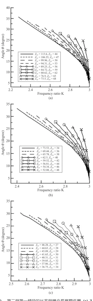
圖 2(a)、(b)、(c)分別為 Z1 = 70.7 Ω、50 Ω及 35.5 Ω的 第一頻段與第二頻段的比值與耦合線電氣長度的關係圖 表。藉由三張圖表可知,當奇模與偶模的特性阻抗 Zoe、Zoo
兩者越為接近或串接的耦合線的電氣長度θ 越小,則第二 頻率點會往三倍頻率點移動,而不同的特性阻抗也會影響 頻率的比值。
運用上述特性圖並事先決定第二頻率點,再計算第二 頻率點與第一頻率點的比值,搭配適當的奇模與偶模特性 阻抗 Zoe、Zoo,可以得到 Y 軸的電氣長度θ,即可設計出所 需的雙頻電路。
三、電路設計與實作
依照上述的設計方式應用於威爾京森功率分配器
(Wilkinson power divider) 和 鼠 圈 式 功 率 分 配 器 (rat-
race),以驗證雙頻段電路設計流程的正確性。
1. 威爾京森功率分配器 (Wilkinson Power Divider) 傳統式威爾京森功率分配器[28],其基本結構為兩段特 性阻抗 70.7 Ω、電氣長度為 90°組合而成。依照上述設計方 式,第一頻率點 f0為 0.915 GHz,給定適當的奇模特性阻抗 Zoo和傳輸線的電氣長度θ2,代入式(6)、(7)、(14)中計算出 其它電路數值和第二頻率點 f,藉由觀察圖 2(a)逐步改變耦 合線長度,使第二頻率點移至所需的頻段上。例如:給定奇 模特性阻抗 Zoo = 44.37 Ω、傳輸線的電氣長度θ2 = 27°,由θ2
= 27° 可求出θ1 = 12°。將 Zoo帶入式(6)中可以求出 Zoe = 112.65 Ω,分別將奇模特性阻抗 Zoo帶入式(7)和偶模特性阻 抗 Zoe帶入式(8),可求得串接耦合線的電氣長度θ = 21.038°。
40
35
30
25
20
15
10
5
2.2 2.4 2.6 2.8 3
Frequency ratio K (a)
Zoe = 113.6, Zoo = 44 Zoe = 106.35, Zoo = 47 Zoe = 99.96, Zoo = 50 Zoe = 94.31, Zoo = 53 Zoe = 89.25, Zoo = 56 Zoe = 84.72, Zoo = 59 Zoe = 80.62, Zoo = 62 Zoe = 76.9, Zoo = 65 Zoe = 73.5, Zoo = 68
35
30
25
20
15
10
5
2.4 2.6 2.8 3
Frequency ratio K (b)
Zoe = 73.53, Zoo = 34 Zoe = 69.44, Zoo = 36 Zoe = 65.78, Zoo = 38 Zoe = 62.5, Zoo = 40 Zoe = 59.52, Zoo = 42 Zoe = 56.81, Zoo = 44 Zoe = 54.34, Zoo = 46 Zoe = 52.08, Zoo = 48
35
30
25
20
15
10
5
2.5 2.6 2.7 2.8 2.9 3
Frequency ratio K (c)
Zoe = 46.28, Zoo = 27 Zoe = 44.63, Zoo = 28 Zoe = 43.09, Zoo = 29 Zoe = 41.65, Zoo = 30 Zoe = 40.31, Zoo = 31 Zoe = 39.05, Zoo = 32 Zoe = 37.86, Zoo = 33 Zoe = 36.75, Zoo = 34
Angle (degree)θAngle (degree)θAngle (degree)θ
圖2 第二與第一頻段的比率與耦合長度關係圖 (a) Z1 = 70.7 Ω (b) Z1 = 50 Ω (c) Z1 = 35.5 Ω
將此數值帶入式(14)中,經過整合計算可得式(15),可得兩 個頻率點分別為 0.915 GHz 和 2.444 GHz。
2 2
2
2
(112.65 44.37tan (22.99 ))
282.8tan(39.34 )tan(22.99 )(112.65 44.37tan (22.99 )) 19993.96tan (22.99 ) 0
f
f f f
f
−
− −
− = (15)
電路實作使用 FR-4 雙面板,基板厚度為 1.6 mm,相 對介電常數為 4.3,loss tangent = 0.02。以電磁模擬軟體 (IE3D) 內含之 Line Gauge 進行電路尺寸結構運算,可得 W1 = 3.1 mm、W2 = 1.64 mm、W3 = 1 mm、L1 = 5 mm、L2
= 2.31 mm、L3 = 1.64 mm、L4 = 1.14 mm、L5 = 0.7 mm、 L6 = 11.53 mm、L7 = 2.92 mm、L8 = 3.1 mm、L9 = 16 mm、 L10 = 2.28 mm、L11 = 1.17 mm、g = 0.2 mm。輸入/輸出埠 之特性阻抗為 50 Ω,電路結構為圖 3(a),實際電路圖如圖 3(b)所示,電路尺寸為 22.48 mm × 37.56 mm,並以向量網 路分析儀 Anritsu-37269D 進行量測。
圖 3(c)為電路之散射參數|S11|、|S21|、|S31|與|S32|模擬與 實際量測結果,實線為實測值、虛線為 IE3D 之模擬值。由 圖 3(c)可觀察出本結構模擬的中心頻率分別為 0.915 和 2.45 GHz,不過第二頻率點在實測上稍微偏高至 2.5 GHz。本結 構的|S21|在第一和第二頻段中心頻率為 0.915 和 2.45 GHz 實 測值為−3.235 dB 和−3.689 dB,|S31|在第一和第二頻段中心 頻率為 0.915 和 2.45 GHz 實測值為−3.235 dB 和−3.689 dB。
圖 3(d)為電路之相位圖,在第一和第二中心頻率為 0.915和 2.45 GHz 之∠S21和∠S31相位分別為−139.65°、
−139.12°和−39.939°、−37.621°,相位差分別為 0.53°和 2.311°,而模擬結果∠S21和∠S31相位分別為−125.8°、
−125.8°和−9.899°、−9.898°,相位差為 0°。
為了考慮製作誤差對電路的特性影響,所以在模擬時 加入不同的間隙 g 值分別為 0.9g、g 以及 1.1g,圖 3(e)為 加入不同 g 值的電路之散射參數|S11|、|S21|的誤差頻率響應 圖,圖 3(f)為|S31|、|S41|之誤差頻率響應圖,圖 3(g)為相位 誤差圖,表一顯示三種不同 g 值對 Wilkinson power divider 的特性影響。
2. 鼠圈式功率分配器 (Rat-Race)
傳統鼠圈式功率分配器 (rat-race) [29],其基本結構是 以三段電氣長度為 90° 和一段電氣長度為 270° 的傳輸線所 組成,電路特性阻抗為 70.7 Ω。依照上述之設計公式設定第 一頻段之中心頻率為 0.915 GHz,並給定適當的奇模特性阻 抗 Zoo和傳輸線的電氣長度θ2,代入式(6)、(7)、(14)中計算 出其它電路數值和第二頻率點 f,藉由觀察圖 2(a)逐步改變 耦合線長度,使第二頻率點移至所需的頻段上。當給定奇模 特性阻抗 Zoo為 47 Ω、傳輸線的電氣長度為θ2 = 30°,由θ2 = 30° 可知θ1 = 10°。將 Zoo帶入式(6)中可以求出 Zoe = 113.6 Ω 再將奇模特性阻抗 Zoo帶入式(7)和偶模特性阻抗 Zoe帶入式 ( 8 ),即可求得串接耦合線的電氣長度θ = 2 2 . 0 6 2 °。
W3
Port 2 W1
W2
W2
L4L5
L6
L9
L10
L8
L11
L7
L1
L3
L2
W2
Port 1 W1
Port 3 g
(a) (b)
2.45 GHz
0.915 GHz
-60 -40 -20 0
Magnitude (dB)
0 1 2 3 4
Frequency (GHz)
[S(1,1)] Simulated g = 0.9 g [S(2,1)] Simulated g = 0.9 g [S(1,1)] Simulated g = 0.2 [S(2,1)] Simulated g = 0.2 [S(1,1)] Simulated g = 1.1 g [S(2,1)] Simulated g = 1.1 g
(e) 0
-20
-40
-60
Magnitude (dB)
0 1 2 3 4
Frequency (GHz) 0.915 GHz
2.45 GHz
|S11| Simulation
|S21| Simulation
|S31| Simulation
|S32| Simulation
|S11| Measurement
|S21| Measurement
|S31| Measurement
|S32| Measurement
(c)
2.45 GHz
0.915 GHz
-50 -30
-40 -20 -10 0
Magnitude (dB)
0 1 2 3 4
Frequency (GHz)
[S(3,1)] Simulated g = 0.9 g [S(3,2)] Simulated g = 0.9 g [S(3,1)] Simulated g = 0.2 [S(3,2)] Simulated g = 0.2 [S(3,1)] Simulated g = 1.1 g [S(3,2)] Simulated g = 1.1 g
(f)
2.45 GHz
0.915 GHz
-300 -200 -100 0 100 200
Magnitude (dB)
0 1 2 3 4
Frequency (GHz)
∠S21 Measurement
∠S31 Measurement
∠S21 Simulation
∠S31 Simulation
(d)
2.45 GHz
0.915 GHz -200
0 200
Phase (degree)
0 1 2 3 4
Frequency (GHz)
Simulated ∠S21 g = 0.9 g Simulated ∠S31 g = 0.9 g Simulated ∠S21 g = 0.2 Simulated ∠S31 g = 0.2 Simulated ∠S21 g = 1.1 g Simulated ∠S31 g = 1.1 g
(g)
圖3 (a) 威爾京森功率分配器電路結構 (W1 = 3.1 mm、W2 = 1.64 mm、W3 = 1 mm、L1 = 5 mm、L2 = 2.31 mm、L3 = 1.64 mm、L4 = 1.14 mm、L5 = 0.7 mm、L6 = 11.53 mm、L7 = 2.92 mm、L8 = 3.1 mm、L9 = 16 mm、L10 = 2.28 mm、L11 = 1.17 mm、g = 0.2 mm) (b) 威爾京森功率分配器電路實體圖 (22.48 mm × 37.56 mm) (c) 雙頻威爾京 森功率分配器之頻率響應 (d) 雙頻威爾京森功率分配器之∠S21與∠S31相位 (e) 不同g值之雙頻威爾京森功率分 配器|S11|與|S21|頻率響應 (f) 不同g值之雙頻威爾京森功率分配器|S31|與|S32|頻率響應 (g) 不同g值之雙頻威爾京 森功率分配器∠S21與∠S31相位圖
表一 不同g值對Wilkinson power divider的影響
g = 0.9g (0.915/2.45 GHz) g = 0.2 (0.915/2.45 GHz) g = 1.1g (0.915/2.45 GHz)
|S11| −39.76 dB/−20.03 dB −54.68 dB/−20.17 dB −32.03 dB/−18.43 dB
|S21| −3.173 dB/−3.28 dB −3.158 dB/−3.268 dB −3.182 dB/−3.31 dB
|S31| −3.172 dB/−3.273 dB −3.156 dB/−3.266 dB −3.183 dB/−3.308 dB
|S32| −22.96 dB/−18.21 dB −21.59 dB/−12.82 dB −22 dB/−17.01 dB
∠S21 −129.7°/−27.55° −125.8°/−9.899° −128.5°/−25.18°
∠S31 −129.6°/−27.49° −125.8°/−9.898° −128.5°/−25.1°
W5
W2
W2
W3
L5
L2
L1
W1
W4
L3
Port 4
L6
L4
W6
Port 2 Port 1
g Port 3
(a)
0
-10
-20
-30
-40
-50
Magnitude (dB)
0 1 2 3 4
Frequency (GHz) 0.915 GHz
2.45 GHz
|S11| IE3D Simulation
|S21| IE3D Simulation
|S11| Measurement
|S21| Measurement
(c)
(b)
0
-20
-40
-60
-80
Magnitude (dB)
0 1 2 3 4
Frequency (GHz) 0.915 GHz
2.45 GHz
|S31| IE3D Simulation
|S41| IE3D Simulation
|S31| Measurement
|S41| Measurement
(d)
圖4 (a) 雙頻鼠圈式功率分配器電路結構 (W1 = 3.1 mm、W2 = 4.72 mm、W3 = 1.43 mm、W4 = 1.27 mm、W5 = 3.09 mm、W6 = 12.4 mm、L1 = 5 mm、L2 = 6.36 mm、L3 = 1.64 mm、L4 = 9.44 mm、L5 = 3.1 mm、L6 = 3.17 mm、
g = 0.29 mm) (b) 雙頻鼠圈式功率分配器電路實體圖 (44.66 mm × 46.27 mm) (c) 雙頻鼠圈式功率分配器|S11|與
|S21|之頻率響應 (d) 雙頻鼠圈式功率分配器|S31|與|S41|之頻率響應。((e)-(h)接續下頁)
將上述數值帶入式(14)中,經過整合計算可得式(16),可得 兩個頻率點分別為 0.915 GHz 和 2.44 GHz。
2 2
2
2
(113.6 47tan (23.99 ))
282.8tan(39.79 )tan(23.99 )(113.6 47tan (23.99 )) 19993.96tan (23.99 ) 0
f
f f f
f
−
− −
− = (16)
電路實作使用 FR-4 雙面板,基板厚度為 1.6 mm,相對 介電常數為 4.3,loss tangent = 0.02。以電磁模擬軟體 (IE3D) 內含之 Line Gauge 進行電路尺寸結構運算,可得 W1 = 3.1mm、W2 = 4.72 mm、W3 = 1.43 mm、W4 = 1.27 mm、W5
= 3.09 mm、W6 = 12.4 mm、L1 = 5 mm、L2 = 6.36 mm、L3 = 1.64 mm、L4 = 9.44 mm、L5 = 3.1 mm、L6 = 3.17 mm、
200
100
0
-100
-200
-300
Phase (degree)
0 1 2 3 4
Frequency (GHz) 0.915 GHz
2.45 GHz
Simulation ∠S21
Simulation ∠S31
Measurement ∠S21
Measurement ∠S31
(e)
0
-20
-40
-60
-80
Magnitude (dB)
0 1 2 3 4
Frequency (GHz) 0.915 GHz
2.45 GHz
[S(3,1)] Simulated g = 0.9 g [S(4,1)] Simulated g = 0.9 g [S(3,1)] Simulated g = 0.2 g [S(4,1)] Simulated g = 0.2 g [S(3,1)] Simulated g = 1.1 g [S(4,1)] Simulated g = 1.1 g
(g) 0
-20
-40
-60
Magnitude (dB)
0 1 2 3 4
Frequency (GHz) 0.915 GHz
2.45 GHz
[S(1,1)] Simulated g = 0.9 g [S(2,1)] Simulated g = 0.9 g [S(1,1)] Simulated g = 0.2 g [S(2,1)] Simulated g = 0.2 g [S(1,1)] Simulated g = 1.1 g [S(2,1)] Simulated g = 1.1 g
(f)
200
0
-200
Phase (degree)
0 1 2 3 4
Frequency (GHz) 0.915 GHz
2.45 GHz
Simulated ∠S21 g = 0.9 g Simulated ∠S31 g = 0.9 g Simulated ∠S21 g = 0.2 g Simulated ∠S31 g = 0.2 g Simulated ∠S21 g = 1.1 g Simulated ∠S31 g = 1.1 g
(h)
圖4 (e) 雙頻鼠圈式功率分配器∠S21與∠S31相位 (f) 不同g值之雙頻鼠圈式功率分配器|S11|與|S21|頻率響應 (g) 不同 g值之雙頻鼠圈式功率分配器|S31|與|S41|頻率響應 (h) 不同g值之雙頻鼠圈式功率分配器∠S21與∠S31相位圖
g = 0.29 mm。輸入輸出埠之特性阻抗為 50 Ω,電路結構為 圖 4(a),實際電路圖如圖 4(b)所示,電路尺寸為 44.66 mm
× 46.27 mm,並以向量網路分析儀 Anritsu-37269D 進行量 測。
圖 4(c)為電路之散射參數|S11|、|S21|模擬與實際量測結 果,實線為實測值、虛線為 IE3D 之模擬值。由圖 4(c)可觀 察出模擬結果的中心頻率分別為 0.915 GHz 和 2.45 GHz,
不過第二頻率點在實測上頻率偏高至 2.53 GHz。本結構的
|S21|在第一和第二頻段中心頻率為 0.915 和 2.45 GHz 實測 值為−3.533 dB 和−5.729 dB。圖 4(d)則顯示|S31|在第一和第 二頻段中心頻率為 0.915 和 2.45 GHz 實測值為−3.242 dB 和−3.307 dB。
圖 4(e) 為電路之相位圖,第一和第二中心頻率為 0.915 和 2.45 GHz,∠S21和∠S31相位分別為−152.67°、
−143.39° 和 −62.54° 、 −33.36° , 相 位 差 分 別 為 9.28° 和
29.18°,而模擬值在第一和第二頻段中心頻率為 0.915 和
2.45 GHz時,∠S21和∠S31相位分別為−116°、−105.2°和 19.54°、50.49°,相位差分別為 10.8°和 30.95°。
為了考慮製作誤差對電路的特性影響,所以在模擬時 加入不同的間隙 g 值分別為 0.9g、g 以及 1.1g,圖 4(f)為加 入不同 g 值的電路之散射參數|S11|、|S21|的誤差頻率響應,
圖 4(g)為|S31|、|S41|誤差頻率響應,圖 4(h)為相位誤差圖,
表二顯示三種不同 g 值對 rat-race 的特性影響。
本文選擇與參考文獻[23]文中所提到之雙頻段設計 進行優劣比較,由於設定頻段相同都為 (0.915/2.45 GHz) 分析較為容易,圖 5(a)為參考文獻[23]之電路實體圖,
圖 5(b)為兩個電路之散射參數|S11|、|S21|頻率響應圖,實 線部份為本文電路之實測值,虛線為參考文獻[23]之實 測值,圖 5(c)為|S31|、|S41|之頻率響應圖,圖 5(d)為相位 圖。
表二 不同g值對rat-race的影響
g = 0.9g (0.915/2.45 GHz) g = 0.2 (0.915/2.45 GHz) g = 1.1g (0.915/2.45 GHz)
|S11| −53.49 dB/−31.29 dB −39.76 dB/−20.03 dB −37.67 dB/−27.74 dB
|S21| −3.303 dB/−3.757 dB −3.173 dB/−3.28 dB −3.274 dB/−3.586 dB
|S31| −3.167 dB/−3.023 dB −3.172 dB/−3.273 dB −3.171 dB/−3.127 dB
|S41| −47.42 dB/−29.33 dB −22.96 dB/−18.21 dB −39.54 dB/−27.86 dB
∠S21 −115.4°/21.13° −129.7°/−27.55° −117.6°/15.86°
∠S31 −104.6°/51.75° −129.6°/−27.49° −106.6°/47.75°
(a)
-30 -20 -10 0
-50 -40
Magnitude (dB)
0 1 2 3 4
Frequency (GHz) 0.915 GHz
2.45 GHz
Reference[23] [S(3,1)] measurement Reference[23] [S(4,1)] measurement [S(3,1)] Measurement [S(4,1)] Measurement
(c)
-30 -20 -10 0
-40
Magnitude (dB)
0 1 2 3 4
Frequency (GHz) 0.915 GHz
2.45 GHz
Reference[23] [S(1,1)] measurement Reference[23] [S(2,1)] measurement [S(1,1)] Measurement [S(2,1)] Measurement
(b)
-200 -100 0 100 200
-300
Phase (degree)
0 1 2 3 4
Frequency (GHz) 0.915 GHz
2.45 GHz
Reference[23] measurement ∠S21 Reference[23] measurement ∠S31 Measurement ∠S21 Measurement ∠S31
(d)
圖5 (a) 單一耦合線之rat-race實體圖 (b) 雙耦合線與單耦合線[23] rat-race |S11|與|S21|之頻率響應圖 (c) 雙耦合線與 單耦合線[23] rat-race之|S31|與|S41|之頻率響應圖 (d) 雙耦合線與單耦合線[23] rat-race之相位圖
四、結 論
本文提出一種雙頻段 (dual band) 電路設計方式,以 串接兩個耦合線 (coupled line) 替換一段傳輸線,並利用 耦合線之耦合效應以獲得雙頻的效果。電路分析容易且設 計簡單,並在威爾京森功率分配器 (Wilkinson power divider) 及鼠圈式功率分配器 (rat-race) 上相對的頻率點 (0.915和 2.45 GHz) 有相當高的一致性,可運用於超高頻
段 (UHF) 無線射頻系統及高頻微波電路中。
參考文獻
1. Mondal, P. and Chakrabarty, A., “Design of Miniaturised Branch-Line and Rat-Race Hybrid Couplers with Har- monics Suppression,” IET Microwaves, Antennas & Prop- agation, Vol. 3, No. 1, pp. 109-116 (2009).
2. Alkanhal, M. A. S., “Reduced-Size Dual Band Wilkinson Power Dividers,” ICCCE International Conference on Computer and Communication Engineering, 2008, Vol. 3, No. 13-15, pp. 1294-1298 (2008).
3. Monti, G. and Tarricone, L., “Reduced-Size Broadband CRLH-ATL Rat-Race Coupler,” 36th European Microwave Conference, Vol. 9, No. 10-15, pp. 125-128 (2006).
4. Khaleghi, A., Azoulay, A., and Bolomey, J. C., “A Dual Band Back Coupled Meanderline Antenna for Wireless LAN Applications,” 2005 IEEE 61st VTC Vehicular Technology Conference, Vol. 1, pp. 226-229 (2005).
5. Kim, M. J., Cho, C. S., and Kim, J., “A Dual Band Printed Dipole Antenna with Spiral Structure for WLAN Application,” IEEE Microwave and Wireless Components Letters, Vol. 15, No. 12, pp. 910-912 (2005).
6. Jou, C. F., Cheng, K.-H., Lin, C.-M., and Chen, J.-L.,
“Dual Band CMOS Power Amplifier for WLAN Ap- plications,” 2005 IEEE International Symposium on Micro-NanoMechatronics and Human Science, Vol. 3, No.
27-30, pp. 1227-1230 (2005).
7. Ma, Z., Kikuchi, K., Kobayashi, Y., Anada, T., and Hagiwara, G., “Novel Microstrip Dual-Band Bandstop Filter with Controllable Dual-Stopband Response,” Asia- Pacific Microwave Conference, Vol. 12, No. 12-15, pp.
1174-1177 (2006).
8. Lai, M.-I. and Jeng, S.-K., “Compact Microstrip Dual- Band Bandpass Filters Design Using Genetic-Algorithm Techniques,” IEEE Transactions on Microwave Theory and Techniques, Vol. 54, No. 1, pp. 160-168 (2006).
9. Wu, Y., Liu, Y., Zhang, Y., Gao, J., and Zhou, H., “A Dual Band Unequal Wilkinson Power Divider without Reactive Components,” IEEE Transactions on Microwave Theory and Techniques, Vol. 57, No. 1, pp. 216-222 (2009).
10. Cheng, K.-K. M. and Wong, F.-L., “A New Wilkinson Power Divider Design for Dual Band Application,” IEEE Microwave and Wireless Components Letters, Vol. 17, No.
9, pp. 664-666 (2007).
11. Avrillon, S., Pele, I., Chousseaud, A., and Toutain, S.,
“Dual-Band Power Divider Based on Semiloop Stepped-Impedance Resonators,” IEEE Transactions on Microwave Theory and Techniques, Vol. 51, No. 4-1, pp.
1269-1273 (2003).
12. Chen, C.-C. and Wang, S.-M., “Design of an LTCC Switchable Filter for Dual-Band RF Front-End Applica- tions,” IEEE Region 10 Conference TENCON 2007, pp.
1-3 (2007).
13. Wu, J., Panagamuwa, C. J., McEvoy, P., Vardaxoglou, J.
C., and Saraereh, O. A., “Switching a Dual Band PIFA to
Operate in Four Bands,” IEEE Antennas and Propagation Society International Symposium 2006, Vol. 7, No. 9-14, pp. 2675-2678 (2006).
14. Guan, X., Ma, Z., Cai, P., Li, G., Kobayashi, Y., Anada, T., and Hagiwara, G., “A Dual-Band Bandpass Filter Synthesized by Using Frequency Transformation and Circuit Conversion Technique,” Asia Pacific Microwave Conference, Vol. 4 (2005).
15. Zhang, H. and Chen, K. J., “A Stub Tapped Branch-Line Coupler for Dual-Band Operations,” IEEE Microwave and Wireless Components Letters, Vol. 17, No. 2, pp.
106-108 (2007).
16. Zhang, H., Peng, Y., and Xin, H., “Design of Dual-Band Balun with Tapped Stubs,” 2008 IEEE Radio and Wireless Symposium, Vol. 1, No. 22-24, pp. 859-862 (2008).
17. Park, M. J. and Lee, B., “A Dual-Band Wilkinson Power Divider,” IEEE Microwave and Wireless Components Letters, Vol. 18, No. 2, pp. 85-87 (2008).
18. Zhou, M., Tang, X., and Xiao, F., “Compact Dual Band Bandpass Filter Using Novel E-Type Resonators with Controllable Bandwidths,” IEEE Microwave and Wireless Components Letters, Vol. 18, No. 12, pp. 779-781 (2008).
19. Mokhtaari, M., Bornemann, J., and Amari, S., “Coupling- Matrix Design of Dual/Triple-Band Uni-Planar Filters,”
IEEE MTT-S International Microwave Symposium Digest, pp. 515-518 (2006).
20. Chuang, M.-L., “Concurrent Dual Band Filter Using Single Set of Microstrip Open-Loop Resonators,” Elec- tronics Letters, Vol. 41, No. 18, pp. 1013-1014 (2005).
21. Zhang, H., Peng, Y., and Xin, H., “A Tapped Stepped- Impedance Balun with Dual-Band Operations,” IEEE Antennas and Wireless Propagation Letters, Vol. 7, pp.
119-122 (2008).
22. Zhang, Y. P. and Sun, M., “Dual-Band Microstrip Bandpass Filter Using Stepped-Impedance Resonators with New Coupling Schemes,” IEEE Transactions on Microwave Theory and Techniques, Vol. 54, No. 10, pp.
3779-3785 (2006).
23. Wu, C. K. and Tseng, J. D., “A Coupled Line Structure for Dual Band Application,” Journal of Technology, Vol. 22, No. 4, pp. 349-355 (2007).
24. Atlasbaf, Z. and Forooraghi, K., “A New Dual Band Branch-Line Coupler Using Coupled Lines,” 7th ISAPE International Symposium on Antennas, Propagation &
EM Theory, pp. 1-4 (2006).
25. Pozar, D. M., Microwave Engineering, Second Edition, Wiley, chap. 2 and 4, USA (1998).
26. Jones, E. M. T., “Coupled-Strip-Transmission-Line Filters
and Directional Couplers,” IRE Transactions on Micro- wave Theory and Techniques, Vol. 4, No. 2, pp. 75-81 (1956).
27. Zysman, G. I. and Johnson, A. K., “Coupled Transmission Line Networks in an Inhomogeneous Dielectric Medium,”
IEEE Transactions on Microwave Theory and Techniques, Vol. 17, No. 10, pp. 753-759 (1969).
28. Wilkinson, E. J., “An N-Way Hybrid Power Divider,” IRE Transactions on Microwave Theory and Techniques, Vol.
8, pp. 116-118 (1960).
29. Reed, J. and Wheeler, G. J., “A Method of Analysis of Symmetrical Four-Port Networks,” IRE Transactions on Microwave Theory and Techniques, Vol. 4, No. 4, pp.
246-252 (1956).
2009年 04 月 24 日 收稿 2009年 05 月 07 日 初審 2009年 07 月 10 日 複審 2009年 08 月 27 日 接受
![圖 5 (a) 單一耦合線之 rat-race 實體圖 (b) 雙耦合線與單耦合線 [23] rat-race |S 11 | 與 |S 21 | 之頻率響應圖 (c) 雙耦合線與 單耦合線 [23] rat-race 之 |S 31 | 與 |S 41 | 之頻率響應圖 (d) 雙耦合線與單耦合線 [23] rat-race 之相位圖 四、結 論 本文提出一種雙頻段 (dual band) 電路設計方式,以 串接兩個耦合線 (coupled line) 替換一段傳輸線,並利用 耦合線之耦合](https://thumb-ap.123doks.com/thumbv2/9libinfo/9126516.410816/8.892.94.797.146.912/單一耦合線之實體雙耦合線與單耦合|S||雙耦合雙耦合線.webp)
