行政院國家科學委員會補助專題研究計畫 ◎ 成 果 報 告
□期中進度報告 低溫多晶矽薄膜太陽電池之研究
計畫類別:◎ 個別型計畫 □ 整合型計畫 計畫編號:96-2221-E-011-054-
執行期間:96 年 8 月 1 日至 97 年 7 月 31 日
計畫主持人:葉文昌 共同主持人:
計畫參與人員: 黃祥恩,陳秉群,戴漢昇,金大為,江信毅
成果報告類型(依經費核定清單規定繳交):◎精簡報告 □完整報告
本成果報告包括以下應繳交之附件:
□赴國外出差或研習心得報告一份
□赴大陸地區出差或研習心得報告一份
◎出席國際學術會議心得報告及發表之論文各一份
□國際合作研究計畫國外研究報告書一份
處理方式:除產學合作研究計畫、提升產業技術及人才培育研究計畫、
列管計畫及下列情形者外,得立即公開查詢
□涉及專利或其他智慧財產權,□一年□二年後可公開查詢 執行單位:
中 華 民 國 97 年 10 月 20 日
1.
Characteristic of TFTs fabricated on location controlled lateral grains
Hsin-Yi Chiang1, Han-Sheng Dai1, Hsin-Chi Chen1,2, Xiang-En Hung1, Chih-Yu Chang1, Wen-Chng Yeh1
1Department of Electronics Engineering, National Taiwan University of Science and Technology, Taipei, Taiwan, 106, R.O.C
2Department of Automatic Engineering, Lan Yang Institute of Technology, I-Lan, Taiwan, 261, R.O.C
n-channel TFTs were fabricated on micro-lens array induced location controlled lateral grains in excimer laser annealing (ELA), with using sputtering deposition method for both Si active layer and SiO2 gate insulator. The TFTs have the best electron field effect mobility of 160 cm2/V-s when the Si film is in slightly completely melting regime in ELA process, with on/off ratio of 105and S value of 1.2 V.
INTRODUCTION
Rapid melting and recrystallization by excimer laser annealing (ELA) of amorphous silicon (a-Si) thin films have been applied to the production of low-temperature polycrystalline silicon (poly-Si) for thin-film transistors (TFTs)1. These TFTs construct not only pixel switches, but also peripheral driver circuits for active-matrix flat-panel displays. Their future evolution aims at the enlargement of the matrix/circuit scale and further system integration into the panel, which require both the enhancement of the TFT performance and device-to-device uniformity. The ultimate TFT is the single grain TFTs where the channel of a TFT was formed within a single grain. Several methods for 2D grain control have been proposed in ELA of Si thin-films, μ-Cz2, phase modulated ELA (PMELA)3, 2D sequential lateral solidification (2D-SLS)4, and TFTs with mobility of as high as above 300 cm2/V-s have been fabricated in these method.
We have proposed micro-lens array induced location controlled lateral grains, and as a result, the super lateral grains (SLG) with a diameter of ~10 µm were formed with a period of 10 µm5,6. In this study, TFTs were fabricated with their channel region formed within a location controlled grain.
Besides, it is worth to say that both the Si active layer and SiO2 gate insulator were formed by sputtering deposition method7,8, and the laser annealing method was used to activate the impurities9.
Experiment a. Crystalline methods
The sample structure was Si(90 nm)/SiO2(100 nm)/SiOxNy(800 nm)/Non
alkali glass in which SiOxNy film work as light absorptive underlayer for increasing the grain size10. Here the Si film was deposited at 250 0C by DC magnetron sputtering deposition method using 105 Ω-cm n-type Fz-Si wafer as the sputtering target. The Si film was then crystallized by ELA method with applying micro-lens array induced grain location control method5.
b. Gate insulators
The gate SiO2 layer was deposited by pulsed-DC reactive magnetron sputtering at room temperature. High quality Si target was used and the atmosphere in the chamber was argon mixed with oxygen. The ratio of oxygen to total gas (4 sccm) was set as 0.5 and the sputter-deposited gas pressure was 5 mTorr.
The power Density was 1.1 W/cm2 and the TON/TOFFwas 5 µs/ 15µs. The MOS capacitor was then annealed at 450 0C in forming gas atmosphere (N2 95%, H2 5%) for 10 min in order to improve the interface state between the Si and SiO2.
c. TFT fabrications
After micro-lens array induced location controlled lateral grains with a diameter of 10 µm. The succeeding TFT fabrication process is as following. Si islands were fabricated by photolithography and successive reactive ion etching (RIE). Then 140 nm-thick SiO2 as gate insulator was formed by pulsed-DC reactive sputtering method. The substrate was not heated during film deposition. Then Al film was deposited by thermal evaporation at room temperature, and was then patterned into gate pattern. Phosphorous was implanted into Si film with a dosage of 5×1015 cm-2and with an implanting energy of 137 keV. The impurity was then activated by room
1E-11 1E-10 1E-09 1E-08 1E-07 1E-06 1E-05
0 2 4 6 8
E (MV/cm)
J(A/cm2)
temperature ELA method. S/D contact holes were formed and then the Al electrodes were evaporated and patterned to form S/D electrode pattern. Finally, the sample was annealed in forming gas atmosphere at 450oC for 10 min.
Results a. Crystallization
Figure 1 shows the Atomic force microscope (AFM) image of the micro-lens array. Figure 2 shows the optical micrograph of Si film after ELA. 10 μm diameter SLG grains were formed with a period of 10 μm.
.
Fig. 1 Atomic force microscope image of the micro-lens array
Fig. 2 Optical micrograph of SLG grain location controlled Si film
b. The electric characteristics of gate SiO2 Figure 3 shows the I-V curve of the sputter-deposited SiO2 films. The breakdown field was as high as 7 MV/cm while the current density reached 1 µA/cm2. Figure 4 shows the C-V curves of SiO2before and after annealing. The curves are shifted rightward and the difference between forward and reverse measurement result is much less. This is due to the defects in the SiO2 layer decreasing after annealing. The oxide fixed charges are down to 1.95×1011cm-2 and the interface state density is ~7×1011cm-2eV-1.
Fig. 3 Current density vs. electric field intensity for sputter-deposited SiO2 films
Fig. 4 The C-V curves of sputter-deposited SiO2and dry thermal oxide
c. The electric characteristics of TFTs
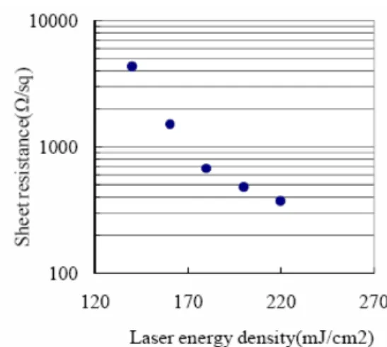
Figure 5 shows the sheet resistance of Si films as a function of excimer laser energy density I. Each position was exposed to 100 pulses of laser light. The sheet resistance decreased with increasing I, and became 370 Ω/sq at I = 220 mJ/cm2. However when I >
160 mJ/cm2, some portion of Si film peeled off, so I was set at 160 mJ/cm2 in TFT fabrication. The sheet resistance of Si film in this energy density is 1500 Ω/sq.
4 types of TFTs were fabricated depending on laser energy density in ELA process in which four regimes were defined. That is, deeply completely melting regime, slightly completely melting regime, partially melting regime, and surface melting regime. Note that only the Si film in slightly completely melting regime did the SLG grains take place and did location of these SLG grains controlled.
Figure 6 shows the Id-Vg characteristics of these TFTs. Electron field effect mobilities in each conditions were also shown in figure. For TFTs in slightly completely melting regime, the field effect mobility is 160 cm2/V-s, on/off
0.3 0.4 0.5 0.6 0.7 0.8 0.9 1 1.1
-10 -8 -6 -4 -2 0 2
Vg (V)
C/Cox
Asdepo sputter SiO2
Dry therm. SiO2
Sputter SiO2 after forming gas 450 ℃, 10 min 10 um
ratio is 105, and S value is 1.2V. The sheet resistance of Si film at S/D region is 1500 Ω/sq, which limited the mobility and on current. Besides, lightly doped n type Si (5-10 Ω-cm) film was used in channel region, which result in higher off current. TFT characteristics will be further improved by optimization of fabrication processes. In the TFTs fabricated on Si films with either highly completely melting regime or partially melting regime, the mobility is decreased, probably due to decreasing of grain sizes. In addition, the grains in these regimes are randomly located.
Fig. 5 Sheet resistance of Si film as a function of laser energy density
Fig. 6 Id-Vg characteristics and mobilities of TFTs
Conclusions
n-channel TFTs were fabricated on micro-lens array induced location controlled lateral grains, with using DC sputtering to form Si films for active layer and using pulsed-DC reactive sputtering to deposit SiO2 films for gate insulator. The Si film in slightly completely melting regime results in the best TFT performance. The electron field effect mobility of as high as 160 cm2/V-s has been obtained, with the on/off ratio of 105, S value of 1.2V. Further improvement can be expected by decreasing sheet resistant of S/D region, by using lightly doped p type Si channel region, and by decreasing interface trap density between Si and SiO2.
Acknowledgement
This research was partially supported by the National Science Council (NSC) of Taiwan under the contract number of NSC
96-2221-E-011-054- and
97-2221-E-011-018-MY2.
References
1. T. Sameshima, S. Usui, and M.
Sekiya,”XeCl Excimer laser annealing used in the fabrication of poly-Si TFT's”, IEEE Electron Device Lett. 7, 276 (1986).
2. P. Ch. van der Wilt, B.D. van Dijk, G. J.
Bertens,
R.Ishihara and C.I.M. Beenakker: Appl.
Phys. Lett. 72, 1819 (2001).
3. Mitsuru Nakata, Kouki Inoue, and Masakiyo Matsumura, Jpn. J. Appl. Phys., 40, 3049 (2001).
4. James S. Im, Robert S. Sposili, and M. A.
Crowder, Appl. Phys. Lett. 70, 3434 (1997).
5. Wen-chang Yeh and Dun-yuan Ke,
“Location control of super lateral growth grains in excimer laser crystallization of silicon thin films by microlight beam seeding”:Jpn. J.Appl. Phys. 45, L970 (2006).
6. Wenchang Yeh, Dunyuan Ke, Chunjun Zhuang, Hsiangen Huang, and Yubang Yang, “Light absorptive underlayer enhanced excimer-laser crystallization of Si thin-film”,J.Mater. Res., 22, 2973(2007).
7. T. Serikawa, "Sputter Deposition of Thin Films for High Mobility Poly-Si TFT Fabrication", Materials Science Forum, 140-142, 387 (1993).
8. T. Serikawa, T. Miyamoto, H. Ueno, Y.
Sugahara, Y. Uraoka, T. Fuyuki,
"Room-temperature sputter-deposited gate SiO2 films for high quality poly-Si TFTs", ECS Transactions 3 (8), 107 (2006).
9. T. Noguchi et. Al, "Effective Dopant Activation in Silicon Film Using Excimer
Laser Annealing for High-Performance Thin Film Transistors", Jpn. J. Appl. Phys.
47, 1858 (2008).
10. Wenchang Yeh et. al., “Light Absorptive
Underlayer Enhanced Super Lateral Growth in Excimer Laser Crystallization of Amorphous Silicon Film”, Jpn. J. Appl. Phys., 46, 1466(2007).