W. C. Lai, Y. K. Su, and S. J. Chang
Institute of Microelectronics and Department of Electrical Engineering, National Cheng Kung University, Tainan 70101, Taiwan, Republic of China
C. J. Kao, C. J. Tun, M. G. Chen, W. H. Chang, and G. C. Chi
Department of Physics, National Central University, Chung-Li 320, Taiwan, Republic of China
J. M. Tsai
South Epitaxy Corporation, Hsin-Shi 744, Taiwan, Republic of China 共Received 30 January 2003; accepted 7 May 2003兲
By using organometallic vapor phase epitaxy we have prepared i-GaN/low temperature共LT兲 GaN/ Ni/Au 共sample A兲 and i-GaN/Ni/Au 共sample B兲 Schottky barrier ultraviolet 共UV兲 photodiodes 共PDs兲. It was found that we could significantly reduce leakage current and achieve a much larger photocurrent to dark current contrast ratio by introducing a LT GaN on top of the conventional nitride-based UV PDs. With an incident light wavelength of 350 nm and a⫺1 V reverse bias, it was found that the measured responsivity was around 0.1 and 0.37 A/W for samples A and B, respectively. Furthermore, it was found that the operation speed of sample A is slower than that of sample B due to the highly resistive LT GaN layer induced large RC time constant. © 2003 American Institute of Physics. 关DOI: 10.1063/1.1587890兴
I. INTRODUCTION
Gallium nitride共GaN兲 is one of the most promising ma-terials for the fabrication of high-sensitivity visible-blind ul-traviolet共UV兲 detectors, since it has a large direct band gap 共3.41 eV at room temperature兲 and a high saturation electron drift velocity 共310 cm/s兲.1 The superior radiation hardness and high temperature共HT兲 resistance of GaN also make it a suitable material for UV detectors working in extreme con-ditions. In the past few years, various types of GaN-based photodetectors have been proposed, such as p⫺n junction photodiodes 共PDs兲,2 p⫺i⫺n PDs,3,4 p⫺⫺n PDs,5 Schottky barrier PDs,6 and metal-semiconductor-metal 共MSM兲 photodetectors.7–9
Compared with p⫺n junction PDs, the fabrication process of Schottky barrier PDs is much easier. The response speed of Schottky barrier PDs is faster. However, leakage current in Schottky barrier PDs is also higher due to the large thermionic emission current in Schottky barrier PDs, as compared to the diffusion current in p⫺n junction PDs for a given built-in voltage. To reduce the leakage current in Schottky barrier PDs, it is necessary to achieve a high Schottky barrier height at the metal/ semiconductor interface. Various metals10–13and transparent conducting oxide films14,15have been deposited on GaN to achieve high performance Schottky barrier PDs. In addition
to the choice of contact metals, leakage current of Schottky barrier PDs also depends strongly on the properties of the topmost semiconductor layer. Previously, it has been shown that one can significantly reduce gate leakage current in GaAs field effect transistors共FETs兲 by utilizing a low tem-perature 共LT兲 GaAs layer.16,17 A similar concept has been applied to GaN-based PDs.18In this study, we deposited a LT GaN layer on top of an undoped i-GaN layer, and fabricated nitride-based UV Schottky barrier PDs with a LT GaN cap layer. The optical and electrical properties of the fabricated PDs will be reported.
II. EXPERIMENT
Samples used in this study were all grown on c-face (0001) sapphire (Al2O3) substrates by organometallic vapor phase epitaxy共OMVPE兲.15After annealing the sapphire sub-strate at 1100 °C in H2 ambient to remove surface contami-nation, a 30-nm-thick, LT GaN nucleation layer was depos-ited onto the sapphire substrate at 560 °C. The temperature was then raised to 1060 °C to grow a 2-m-thick Si-doped n⫹-GaN (n⫽3⫻1018cm⫺3) layer. On top of this n⫹-GaN layer, we subsequently grew a 0.3-m-thick undoped GaN 共i-GaN兲 followed by a 30-nm-thick LT GaN as the cap layer 共i.e., sample A兲. The growth temperature of the LT GaN cap layer was 550 °C. It should be noted that this LT GaN cap layer behaves like an insulator with a sheet resistivity larger than 109⍀/䊐, in excess of the measurement limitation of
a兲Author to whom correspondence should be addressed; electronic mail:
1753
our instrument. Samples without the LT GaN cap layer were also prepared for comparison 共i.e., sample B兲. As shown in Fig. 1, nitride-based Schottky barrier PDs were then fabri-cated by dry etching,19 deposition of Ti/Al on exposed n⫹-GaN as ohmic contact, deposition of semitransparent Ni/ Au共3 nm/10 nm兲 on LT GaN as Schottky barrier metal,20and deposition of Ti/Au共50 nm/1m兲 on Ti/Al and Ni/Au to serve as the bonding pad. The diameter of the fabricated circular PDs was kept at 500 m. Room temperature current–voltage (I⫺V) characteristics of the fabricated PDs were then measured by a HP4156 semiconductor parameter analyzer. Spectral responsivity of these Schottky barrier PDs was also measured using a Xe arc lamp and a calibrated monochromator as the light source. Output power of the monochromatic light was measured with a calibrated Si pho-todiode and then illuminated onto the front side of PDs. Transient response was also evaluated by using a 337 nm N2 laser with a 0.5 ns excitation pulse to optically excite the fabricated PDs. A 500 MHz oscilloscope with a 1000⍀ load resistance was then used to measure the impulse response.
III. RESULTS AND DISCUSSION
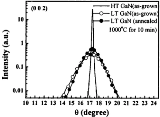
It is known that as-grown LT共lower than 300 °C兲 GaAs is conductive (⬃10 ⍀ cm) with a poor crystal quality due to the excess As, which acts as point defects 共i.e., anti sites, AsGa, and interstitial defects兲. It is also known that one can drastically change the electrical properties of LT GaAs by postgrowth thermal annealing. It has been shown that one could increase the resistivity of LT GaAs from⬃10 ⍀ cm to ⬎106⍀ cm by high temperature postgrowth thermal anneal-ing共i.e., ⬎600 °C). 21To clarify if LT GaN is similar to LT GaAs, we performed the following experiments. Figure 2 shows x-ray diffraction共XRD兲 spectra of as-grown LT GaN, annealed LT GaN, and GaN grown at 1060 °C 共i.e., HT GaN兲. The annealing of LT GaN was performed at 1060 °C for 10 min in N2 ambient. It can be seen that XRD peak of LT GaN and annealed LT GaN was much broader with a large full width at half maximum共FWHM兲, as compared to the HT GaN. Such an observation indicates that high tem-perature postgrowth thermal annealing has almost no effect on the crystal quality of LT GaN. On the other hand, our Hall measurement shows that resistivity of LT GaN with and without high temperature annealing was extremely high共i.e., higher than our measurement limit of 109⍀/䊐). In other words, LT GaN seems to be very stable and no property
change could be observed even with a 1000 °C postgrowth thermal annealing. We could thus use this highly resistive LT GaN as the insulator of metal-insulator-semiconductor 共MIS兲-like Schottky barrier PDs. Figure 3 shows the I⫺V curves taken in the dark and under illumination ( ⫽350 nm) for samples A and B. Under reverse bias, it was found that the dark current was near a constant of around 1 ⫻10⫺10A for sample A. In contrast, dark current of sample
B was much larger, and increased rapidly as the reverse bias increased. This could be attributed to the fact that the highly resistive LT GaN cap layer between Ni/Au and i-GaN could result in a thicker and higher potential barrier, as compared to conventional Schottky barrier PDs 共i.e., sample B兲. In other words, leakage current in GaN Schottky barrier PDs with a LT GaN cap layer共i.e., sample A兲 was much smaller and less dependent on the applied reverse bias. The near constant ultrahigh resistance of sample A is also a plus when the PDs are connected to the readout circuits in focal plane arrays. Under illumination, one can see that the much larger photocurrent to dark current contrast ratio could be achieved in sample A due to its low dark current. For example, the contrast ratios were around 2.1⫻104 and 1.7⫻103 for samples A and B, respectively, when the samples were biased at⫺5 V. Under forward bias, it was found that turn-on volt-age of samples A and B was 4.5 and 0.9 V, respectively. The high turn-on voltage observed from sample A could be attrib-uted to its high barrier height and the fact that injected car-FIG. 1. Schematic structure of the n⫹-GaN/i-GaN/LT GaN/Ni/Au Schottky
barrier diode共sample A兲.
FIG. 2. X-ray diffraction共XRD兲 spectra of as-grown LT GaN, annealed LT GaN, and high temperature grown GaN共HT GaN兲.
FIG. 3. I⫺V curves taken in dark and under illumination (⫽350 nm) for samples A and B.
riers are compensated by poor crystal quality related trap levels within the band gap of LT GaN. Under forward bias, trap levels in LT GaN are filled by forward carrier injection. Therefore LT GaN will become less insulating. Thus, a sharp rise in forward current can be observed as the forward bias increase over the trap-filled-limit voltage,22VTFL, which de-pends on the thickness and trap density of LT GaN layer. It should be noted that LT GaN is very different from LT GaAs. It is known that as-grown LT GaAs is very conductive with carrier transport dominated by carrier hopping through deep defect bands.5 On the other hand, annealed LT GaAs be-comes highly resistive. Thus, annealed LT GaAs is suitable to serve as the buffer layer in metal-semiconductor FETs or as the gate insulator layer in metal-insulator-semiconductor FETs 共MISFETs兲. In contrast, our preliminary results show that no significant difference in resistivity can be observed between the as-grown LT GaN and the annealed LT GaN. We would like to suggest that more detailed studies should be performed to inspect the annealing effects on the micro-scopic structures of LT GaN.
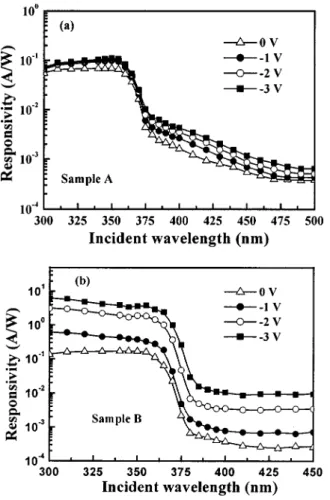
Figures 4共a兲 and 4共b兲 show the spectral response of samples A and B, respectively. It was found that cutoff oc-curred at around 365 nm 共the absorption edge of GaN兲 for both samples. With incident light wavelength of 350 nm and a⫺1 V reverse bias, it was found that the measured respon-sivity was around 0.1 and 0.37 A/W for samples A and B, respectively. Such a dramatic difference could be attributed
to the fact that incident photons (⫽350 nm) are partially absorbed by the LT GaN cap layer and the photogenerated carriers will compensate trap levels in LT GaN. As a result, the photocurrent and responsivity will both become smaller for sample A. It was also found that the responsivity de-creased slowly as the wavelength of the incident light in-creased from 380 to 480 nm for sample A. In contrast, the responsivity of sample B in this wavelength region was near a constant. The below band gap absorption observed from sample A could again be attributed to the defect levels within the band gap of LT GaN cap layer. Photons in this wave-length region could still excite electrons from deep levels to conduction band, or excite electrons from valence band to deep levels in sample A. Figure 5 shows room temperature transmission spectra of a 500-nm-thick LT GaN layer and a 2-m-thick HT GaN layer grown on sapphire substrates. It should be noted that the intensity modulations observed in the long wavelength region were originated from the forma-tion of microcavity in between GaN-air and GaN-sapphire interfaces. Such an observation also suggests that the sur-faces were reasonably smooth for the samples. The much more significant intensity modulation and the observation of a steep transition edge at around 365 nm共i.e., 3.4 eV兲 both indicate that the crystal quality of the 2-m-thick HT GaN layer is high. In contrast, a much broader transition region in between 380 and 480 nm was observed from the 500-nm-thick LT GaN layer. This broad transition region also agrees well with the responsivity measurement of sample A shown in Fig. 4共a兲. From the large XRD FWHM and the broad transition region, one can thus conclude that many structure defect induced trap levels indeed exist in the LT GaN layer. Returning to Fig. 4共a兲, it is worth noting that, although the response in the short-wavelength side was almost indepen-dent of the applied bias, the responsivity in between 380 and 480 nm increased as the reverse bias共i.e. the applied electric field兲 was increased. Such an increase could be attributed to the tunneling assisted absorption in LT GaN layer under high electric field, since most voltage drop occurred in the highly resistive LT GaN layer in sample A. In other words, the electric field in the LT GaN cap layer is much larger than that in the underlying layer. Thus, tunneling assisted absorption involving trap levels in the LT GaN layer will occur even
FIG. 4. Spectral responsivity of共a兲 sample A and 共b兲 sample B measured at different reverse biases.
when the incident photon energy is smaller than the band gap energy of GaN.23Response in the short-wavelength side共i.e., shorter than 360 nm兲 was almost independent of applied bias and could also be attributed to the fact that most voltage drop occurred in the LT GaN layer rather than in the thicker un-doped GaN layer. In contrast, the much stronger bias depen-dent responsivity of sample B suggests that there might exist some internal gain in this particular Schottky barrier PD, even at low biases. The exact origin of this internal gain is not clear yet. One possible origin of this photoconductive gain is the long lifetimes of carrier in the surface defects of sample B. If this is the case, our result seems to imply that LT GaN cap layer could effectively passivate surface defects on the undoped GaN layer. However, this statement is slightly speculative. Further studies need to be performed to clarify this point.
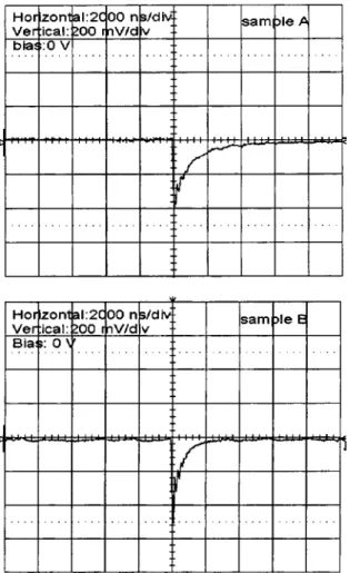
Figure 6 shows the typical transient responses when samples A and B were biased at 0 V. It can be seen that the amplitudes of impulse responses in these samples decreased exponentially with impulse FWHM of around 0.6 and 0.4s for samples A and B, respectively. These results suggest that the operation speed of the fabricated PDs should be limited by the RC time constant of the devices. Figure 7 shows the capacitance–voltage (C⫺V) measurement of the two samples. Under zero bias, it was found that the measured capacitance of samples A and B is around 65 and 84 pF,
respectively. The smaller total capacitance of sample A is attributed to the introduction of LT GaN layer and thus an additional capacitance, CLT, in series with the original de-vice. Although the total capacitance of sample A is smaller, its series resistance should be much larger than that of sample B due to the introduction of highly resistive LT GaN layer. Thus, the operation speed of sample A is slower than that of sample B. In other words, although we could signifi-cantly reduce leakage current and achieve a much larger pho-tocurrent to dark current contrast ratio by introducing a LT GaN on top of the conventional nitride-based UV PDs, op-eration speed of the i-GaN/LT GaN/Ni/Au Schottky barrier PDs is slower than the conventional i-GaN/Ni/Au Schottky barrier PDs.
IV. CONCLUSION
In summary, i-GaN/LT GaN/Ni/Au 共sample A兲 and i-GaN/Ni/Au共sample B兲 Schottky barrier UV PDs were pre-pared by OMVPE. It was found that we could significantly reduce leakage current and achieve a much larger photocur-rent to dark curphotocur-rent contrast ratio by introducing a LT GaN on top of the conventional nitride-based UV PDs. With inci-dent light wavelength of 350 nm and a⫺1 V reverse bias, it was found that the measured responsivity was around 0.1 and 0.37 A/W for samples A and B, respectively. Further-more, it was found that the operation speed of sample A is slower than that of sample B due to the highly resistive LT GaN layer induced large RC time constant.
ACKNOWLEDGMENT
The authors would like to acknowledge the financial support from the National Science Council for their research Grant Nos. NSC 90-2215-E-008-043 and NSC 90-2112-M-008-046.
1J. I. Pankove, Mater. Res. Soc. Symp. Proc. 162, 515共1990兲. 2
E. Monroy, E. Mun˜oz, F. J. Sa´nchez, F. Calle, E. Calleja, B. Beaumout, P. Gibart, J. A. Mun˜oz, and F. Cusso´, Semicond. Sci. Technol. 13, 1042 共1998兲.
3G. Parish, S. Keller, P. Kozodoy, J. A. Ibbetson, H. Marchand, P. T. Fini,
S. B. Fleischer, S. P. DenBaars, and U. K. Mishra, Appl. Phys. Lett. 75, 247共1999兲.
4E. Monroy, M. Hamilton, D. Walker, P. Kung, F. J. Sa´nchez, and M.
Razeghi, Appl. Phys. Lett. 74, 1171共1999兲.
FIG. 6. Typical temporal responses of samples A and B measured at a zero bias.
10X. A. Cao, S. J. Pearton, G. Dang, A. P. Zhang, F. Ren, and J. M. Van
Hove, Appl. Phys. Lett. 75, 4130共1999兲.
11Q. Z. Liu, L. S. Yu, S. S. Lau, J. M. Redwing, N. R. Perkins, and T. F.
Kuech, Appl. Phys. Lett. 70, 1275共1997兲.
12
L. Wang, M. I. Nathan, T.-H. Lim, M. A. Khan, and Q. Chen, Appl. Phys. Lett. 68, 1267共1996兲.
13C. T. Lee, Y. J. Lin, and D. S. Liu, Appl. Phys. Lett. 79, 2573共2001兲.
20J. K. Sheu, Y. K. Su, G. C. Chi, M. J. Jou, C. M. Chang, C. C. Liu, W. C.
Hung, J. S. Bow, and Y. C. Yu, J. Vac. Sci. Technol. B 18, 729共2000兲.
21D. C. Look, D. C. Walters, M. O. Manasreh, J. R. Sizelove, C. E. Stutz,
and K. R. Evans, Phys. Rev. B 42, 3578共1990兲.
22
M. Lampert and P. Mark, Current Injection in Solids共Academic, New York, 1970兲.