Influence of RF Bias on Hydrogenated Amorphous Silicon
by High-Density Plasma Chemical Vapor Deposition
Wen-Chu Hsiao,aChuan-Pu Liu,aand Ying-Lang Wangb,c,z a
Department of Materials Science and Engineering, Center for Micro-Nano Science and Technology, National Cheng Kung University, Tainan 70101, Taiwan
b
College of Science and Engineering, National University of Tainan, Tainan 700, Taiwan c
Department of Applied Physics, National Chia-Yi University, Chia-Yi 6004, Taiwan
We investigate the microstructure and thermal stability of hydrogenated amorphous silicon 共a-Si:H兲 thin films deposited by high-density plasma chemical vapor deposition共HDP-CVD兲 with various biases using radio frequency 共rf兲 power. The a-Si:H films were prepared without external heating at a high rf power density of 3.18 W/cm2, with the rf power bias varying from 0 to 200 W. Because sputtering also occurs during deposition, hydrogen may be present in a variety of bonding configurations in the a-Si:H films with various biases. Fourier transform infrared spectra show that the HDP-CVD a-Si:H films possess more hydrogen content as well as Si–H2stretching modes than the conventional plasma-enhanced CVD counterpart. The surface morphology of the films becomes smooth upon ion bombardment under rf bias. In addition, variations of the film stress against temperature correlate to the hydrogen desorption at different stages during thermal annealing. More importantly, the different Si–Hxbonding configurations affect the crystallization behavior upon thermal annealing.
© 2007 The Electrochemical Society. 关DOI: 10.1149/1.2713723兴 All rights reserved.
Manuscript submitted October 12, 2006; revised manuscript received January 11, 2007. Available electronically March 20, 2007.
Hydrogenated amorphous silicon共a-Si:H兲 thin films have been widely used in thin-film transistors共TFTs兲, solar cells, and optoelec-tronic devices.1-5 Microstructure and stability of a-Si:H vary with deposition methods and growth conditions due to its structure flex-ibility. Despite its amorphous character, a-Si:H has an optical gap and shows photoconductivity, which can also be varied by doping with boron or phosphorous, analogous to crystalline semiconduc-tors. The properties of a-Si:H are influenced by the amount of hy-drogen bound to the silicon network, which in turn is controlled by the substrate temperature and the hydrogen-silicon surface chemis-try involved in the growth. Deposition techniques that are used for growing a-Si:H films include plasma-enhanced chemical vapor deposition共PECVD兲, electron cyclotron resonance CVD, hot-wire CVD, and reactive magnetron sputtering. A-Si:H films have been most commonly fabricated by PECVD with radio frequency 共rf兲 glow-discharge decomposition of SiH4at 13.56 MHz. However, the deposition rate for high-quality films is rather limited, typically in the range of 0.1–0.5 nm/s.6The easiest method to increase the depo-sition rate in CVD is by increasing the power density. However, the properties may deteriorate, as it is known that high rf power tends to increase the probability of plasma polymerization reactions,7which were found to be the dominant homogeneous process controlling the microstructure, hydrogen content, and bonding properties of the films. There are studies showing that increasing the rf power first leads to a deterioration and then to an improvement of the a-Si:H film properties as the deposition rate increases.6,7
High-density plasma共HDP兲 is a type of advanced CVD technol-ogy in which the density of the plasma is higher共1011–1012n/cm3兲 than that used in conventional PECVD 共108to 1010n/cm3兲. This high ion density enables the HDP-CVD technology to integrate a powerful sputtering process into the deposition while still maintain-ing acceptable net deposition rates. In addition, when an electrical rf power bias is applied to the substrate during deposition, the sputter-ing is enhanced and the film properties change, phenomena which have not been examined before. In this paper, we report on the effect of rf power bias on the properties of the a-Si:H films deposited by HDP-CVD, including bonding configurations, thermal stresses, and surface morphologies, which are compared to those properties on film produced by the conventional PECVD. Furthermore, the crys-tallization behavior of the films is examined upon annealing. We also provide a method to determine the microstructure transforma-tion from the film stress variatransforma-tion.
Experimental
The a-Si:H films were deposited by a HDP-CVD system oper-ated with the gas sources of SiH4and Ar at flow rates of 45 and 115 sccm, respectively. p-Type Si共100兲 wafers of 200 mm diameter and 725m thickness were used as the substrates for all films on which stress measurements were performed. The thickness of the a-Si:H films was measured by spectroscopic ellipsometry. The working pressure of the deposition chamber was 20 mTorr, and the rf power density was 3.18 W/cm2, while the bias power was varied from 0 to 200 W with a step size of 100 W. The bias rf system of HDP-CVD is connected to the cathode and an electrical rf power bias was applied to attract the ions in order to adjust the ion bom-bardment during deposition. In order to make a fair comparison between films, the film thickness was fixed at 250 ± 10 nm. For comparison, an a-Si:H film was also deposited by capacitively coupled rf 共13.56 MHz兲 PECVD operated with an rf power of 140 W at the working pressure of 4 Torr, and the rf power density was 0.45 W/cm2. Under this condition, the film had a similar depo-sition rate to that deposited by HDP-CVD. The depodepo-sition tempera-tures of a-Si:H films in HDP-CVD and PECVD were 370 and 400°C, respectively. Fourier transform IR spectroscopy共FTIR兲 was used to study the bonding configurations of the films, and a bare silicon substrate was scanned to obtain a reference spectrum.
A commercial curvature measurement tool 共Frontier Semicon-ductor Measurements, FSM900TC兲 was used to examine film stress in situ, in which the wafer was heated from 25 to 600°C by six tungsten-halogen lamps at a heating rate of 10°C/min in an evacu-ated chamber at⬃10−6Torr. The stress was determined by measur-ing the change of the substrate curvature induced by the deposited layer. During annealing, thermal desorption spectrometry共TDS兲 was employed to in situ monitor molecular desorption behavior for ma-terial stability as a function of temperature. The surface morphology of each sample was scanned by atomic force microscopy共AFM兲 on a 1⫻ 1 m area at the scan rate of 1 Hz. The structural character-istics were investigated by Raman spectrometry.
Results and Discussion
In amorphous silicon, H atoms are bonded to Si orbitals, i.e., Si–H bonds, having a binding-energy of ⬃3 eV, considerably greater than that of Si–Si bonds.8This is why hydrogen easily re-sides in an a-Si film. Figure 1 shows FTIR spectra for the bonding configurations of the a-Si:H films deposited by HDP-CVD at differ-ent bias powers compared with those deposited by the convdiffer-entional PECVD. The phonon modes can be divided into three groups, which are located at 2000–2200, 840–900, and⬃630 cm−1in Fig. 1a-c,
z
respectively. The first group in Fig. 1a consists of two stretching vibration modes located at 1990–2000 cm−1for Si–H bonding and at 2080–2100 cm−1for Si–H
2bonding. The results show that hydro-gen is mainly bonded as an isolated monohydride in the PECVD a-Si:H film compared to the Si–H2stretch mode in the HDP-CVD films, which might arise from polyhydrides, clustered hydrogen, and Si–H2bonds.9-11 Many reports have revealed that the predominant bonding environment for the hydrogen clusters is of four to seven atoms and divacancies have been proposed as possible configura-tions for these hydrogen clusters in the a-Si:H network.5,10,12
Smets et al.10,12also determined the silicon hydrides Si–Hn共n = 1 or 2兲 at void surfaces by means of the high stretching mode 共2070–2100 cm−1兲 with higher hydrogen concentration. The second group in Fig. 1b shows the spectra of the samples from the Si–H2 bending vibration modes, which can be further divided into the Scis-sors mode at 890 cm−1and the Wagging mode at 850 cm−1. The results coincide with the previous results in that the HDP-CVD a-Si:H films contain a significant amount of the Si–H2 bonding while the PECVD a-Si:H film does not. Moreover, the trend of decreasing the peak intensity with increasing bias power for the samples deposited by HDP-CVD is also consistent with the previous results in Fig. 1a. Therefore, the a-Si:H films deposited in high-density plasma environment would contain a large amount of dihy-drides, but these would decrease with increasing rf power bias. This suggests that the rf power bias enhances the effect of ion bombard-ment and raises the ionization. The third group in Fig. 1c is a broad-ened peak located at⬃640 cm−1for the Si–H wagging mode, where every H bonded to silicon contributes to this mode and conse-quently, this peak is used to determine the hydrogen density.10The total hydrogen concentration is higher in the HDP-CVD films but is slightly influenced by the rf power bias. The FTIR results clearly show that the bonding characteristics and thus, microstructure of the a-Si:H films vary with the deposition method and conditions.
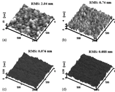
Figure 2 shows atomic force microscopy共AFM兲 images of the surface morphology of the a-Si:H films deposited by PECVD and HDP-CVD with rf power bias. It can be seen clearly that compared to the PECVD film, the HDP-CVD film at zero bias has a higher roughness, which is reduced to significantly less than that of the PECVD film and even decreases significantly with the rf bias. The a-Si:H film deposited in high-density plasma would increase the deposition rate, leading to surface valleys. The surface valleys that cause the high surface roughness might finally evolve into nanosized voids in the bulk during film growth, which may have a deleterious effect on the film properties. The void incorporation is controlled by the competition between the diffusivity of surface species and the arrival rate of the growth precursor at the surface.12When increasing the rf power bias, the sputtering rate increases, leading to the smooth surface and densified structure. In advanced manufacturing, while a smooth surface is required for thin-film transistors, rougher surfaces are useful in solar cells for their higher light trapping.
In order to further verify the bonding configurations of hydrogen in the Si network and thermal stability of the a-Si:H films, TDS was used and the results are shown in Fig. 3, where H2, Si–H, and Si–H2 Figure 1. FTIR spectra of the a-Si:H films deposited by PECVD and
HDP-CVD for共a兲 Si–H stretching mode 共2000–2100 cm−1兲, 共b兲 bending scissor mode共840–890 cm−1兲, and 共c兲 Si–H wagging mode 共⬃630 cm−1兲.
Figure 2. AFM images showing the surface morphology of the as-deposited a-Si:H films deposited by共a兲 PECVD, and HDP-CVD with rf power bias of 共b兲 0, 共c兲 100, and 共d兲 200 W.
desorption spectra are monitored in the channels of 2共Fig. 3a兲, 29 共Fig. 3b兲, and 30 amu 共Fig. 3c兲 from 25 to 600°C, respectively. By comparing the integrated area under each curve between different samples, Fig. 3a shows that a larger amount of hydrogen was re-leased from the a-Si:H films deposited by HDP-CVD than by PECVD. However, upon examining the details of the curves, the
entire hydrogen evolution for these samples behaves very differ-ently. First, hydrogen desorption from the PECVD sample starts at around 250°C, indicating that the a-Si:H films are stable below this temperature, consistent with the results reported in Ref. 4. Between 250 and 600°C, the PECVD a-Si:H was decomposed by the desorp-tion of H2 共Fig. 3a兲 and Si–H 共Fig. 3b兲 throughout the film. The second type is the HDP-CVD sample with zero rf power bias, where Fig. 3a shows an extended H2desorption peak from 170 to 600°C which is attributed to the clustered hydrogen trapped in the Si network.3,4In addition, both the Si–H共Fig. 3b兲 and Si–H2共Fig. 3c兲 desorption spectra show a peak around 280°C, apparently from the bonded Si–Hn共n = 1 − 2兲 groups.3,4The third type of the hydrogen desorption spectra is the HDP-CVD samples with rf power bias, shown as the solid curves in Fig. 3a. Comparing the H2and hydride desorption curves with the FTIR spectra, the complicated hydrogen desorption curve in this case might be attributed to three types of hydrogen compounds. The first peak occurring between 150 and 250°C has been suggested to be from polysilane-like structures with hydrogen-rich intercolumnar regions, which results in the clustering of H2.13The second peak, occurring during the range from 250 to 400°C, corresponds to hydrogen elimination from the regions in the amorphous network that contains hydrogen atoms in close proximity to each other or involving hemolytic rupture of Si–H2bonds yield-ing atomic hydrogen共Fig. 3c兲. The third hydrogen desorption peak, occurring at⬃525°C, can be attributed to the Si–H groups embed-ded in the a-Si:H film and on the a-Si:H/Si interface.4The hydrogen desorption from Si–H happens later than that from Si–H2due to the higher activation energy involved in the hydrogen decomposition of Si–H共295 kJ/mol兲 than that of Si–H2共153 kJ/mol兲. The absence of the Si–H2desorption in the HDP-CVD films with rf power bias in Fig. 3c might be related to the dense structure.
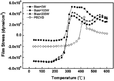
One of the important properties of hydrogen in amorphous sili-con is induced crystallization.14,15Sriraman et al.14has reported that crystallization is mediated by the insertion of H atoms into strained Si–Si bonds as the hydrogen atoms diffuse through the film, where the presence of hydrogen leads to disorder-to-order transitions by annihilating the strained Si–Si bonds in the a-Si:H film. Therefore, the microstructure evolution of the a-Si:H films with temperature was performed to realize the crystallization process. The stress of the a-Si:H films was first examined from 25 to 600°C by the varia-tion of the curvature, as shown in Fig. 4. The initial stress of the HDP-CVD a-Si:H film without rf bias共square兲 is closest to neutral, which might arise from the formation of microvoids and the SiH2 bonds. The HDP-CVD a-Si:H films with rf power bias exhibit com-pressive stress, which might be attributed to Si or H atoms intro-duced by ion bombardment or H2 molecules trapped inside the Figure 3. Thermal desorption spectra of共a兲 hydrogen, 共b兲 monohydride, and
共c兲 dihydride, which were monitored in the channels of 2, 29, and 30 amu from 25 to 600°C, respectively, for a-Si:H films deposited by PECVD and HDP-CVD.
Figure 4. Film stress of the a-Si:H films deposited by PECVD and HDP-CVD as a function of temperature from 25 to 600°C.
a-Si:H films. Comparing the film stress variation with the hydrogen desorption spectra, it can be found that hydrogen concentration in the Si network strongly affects the film stress. The irregular inflec-tion of the temperature variainflec-tion of the a-Si:H film stress has been ascribed to not only the variation of thermal expansion coefficient 共CTE兲 but also structure or density mismatches between the film and substrate.16,17However, the stress changes from compressive to ten-sile drastically at⬃280°C for all the HDP-CVD samples, meaning that the silicon film itself shrinks during the crystallization. There are two possible mechanisms for the volumetric shrinkage of the film. One is the degassing of the incorporated hydrogen, which oc-curs at roughly the same temperature from the hydrogen desorption spectra in Fig. 3a. The other is the reordering of the bond angle during crystallization.17 When the temperature increases above 350°C the atomic structure rearrangement into the crystalline phase is likely to happen, and this could be responsible for stress relax-ation. A similar phenomenon appears for the PECVD sample, where the inflection point is delayed to a higher temperature of⬃400°C. According to the results shown in thermal desorption spectra共Fig. 3兲, the film stress change should be related to the desorption of the monohydride embedded in the a-Si:H film. From the results of the film stress as a function of temperature, the microstructure of the a-Si:H films deposited by PECVD is different from that of films deposited by HDP-CVD.
The intensity of Raman scattering is sensitive to the degree of the structural disorder in solids, so this method can be used to measure relative fractions of the amorphous to the crystalline phases. Figure 5 shows Raman spectra in the range of 350–650 cm−1 from the as-grown a-Si:H films deposited by PECVD and HDP-CVD with various rf power biases, as well as the annealed films at the peratures of 250 and 350°C for 1 h. The selected annealing tem-peratures correspond to the abnormal points on the film stress varia-tion shown in Fig. 4. The Raman spectra exhibit two characteristic peaks, including a single sharp peak at about 520 cm−1and a broad peak around 475 cm−1, corresponding to crystalline and amorphous silicon, respectively. The more pronounced peak at 520 cm−1for all the HDP-CVD films indicates that the microcrystalline grains are embedded in the as-deposited films.18Previous works deemed that Si–H2 and Si–H3 are the main bonding modes for the interface between grains inc-Si:H film.18,19Compared with the FTIR spec-tra, the Si–H2 stretching configuration is observed with increasing crystalline fraction and it is believed that hydrogen is mainly bonded at the grain boundary to passivate the dangling bond. Therefore, the a-Si:H film deposited by HDP-CVD had more microcrystalline structure than by PECVD. The broad peak might be composed of two peaks, where one is the amorphous Si peak at 475 cm−1and the other is located at 490–496 cm−1, assigned to a crystalline-like structure. Therefore, the ratio of amorphous to crystalline structure
stress with Raman spectrum as a function of temperature.
Conclusions
We have examined the properties, such as bonding configuration, hydrogen desorption, stress, and surface morphology of as-deposited a-Si:H films deposited by HDP-CVD with various biases compared with films deposited by PECVD. The FTIR spectra show almost similar bonding configurations in all the samples deposited by HDP-CVD, but they differ from these deposited by PECVD. Therefore, comparing the thermal desorption results with the FTIR spectra, the majority of Si–H with few Si–H2bonds are embedded in the bulk a-Si:H film deposited by PECVD. The higher peak intensity of the stretch mode at 2080–2100 cm−1of the samples deposited by HDP-CVD is mainly due to the dihydride and clustered hydrogen in the bulk and surface, but the concentration of the dihydride decreases with increasing rf power bias. Because the rf power bias enhances the ionization energy and ion bombardment, which can break the Si–H2bonds more easily than that without rf power bias. In addi-tion, the surface morphology of the HDP-CVD a-Si:H films with bias also showed improved surface flatness under ion bombardment. The film stress variation indicates that the HDP-CVD a-Si:H films have a smaller activation energy for crystallization because the bonded hydrogen is desorbed at a lower temperature. The blue shift of the broad peak 共475–496 cm−1兲 of the Raman spectra in the HDP-CVD a-Si:H films with increasing rf power bias suggests that the crystalline-like structure embedded increases with ion bombard-ment. After annealing, the broad peak of all the HDP-CVDa-Si:H films with bias shifts toward 485 cm−1, indicating that while the amorphous structure remains, some of the embedded crystalline-like structure has transformed into the crystalline phase. The microstruc-ture transformation of the a-Si:H films varies with different meth-ods, as evidenced from the Raman spectra, which can correspond to the variations of the film stress. The properties of the a-Si:H films deposited by HDP-CVD are different from those for the films de-posited by PECVD, and the effect of rf power bias is significant on the microstructure.
Acknowledgment
This work was supported by National Science Council of Tai-wan, contract no. NSC-94-2216-E006013, and also partly funded by Applied Materials, Taiwan. The authors thank the Core Facilities Laboratory in Kaohsiung-Pingtung Area, Taiwan, for equipment ac-cess and technical support.
National Cheng Kung University and National Science Council assisted in meeting the publication costs of this article.
References
1. K.-S. Nam, Y.-H. Song, J.-T. Beak, H.-J. Kong, and S.-S. Lee, Jpn. J. Appl. Phys.,
Part 1, 32, 1908共1993兲.
2. J. O. Orwa, J. M. Shannon, R. G. Gateru, and S. R. P. Silva, J. Appl. Phys., 97, 023519共2005兲.
3. H. Y. Kim, J. B. Choi, and J. Y. Lee, J. Vac. Sci. Technol. A, 17, 3240共1999兲.
4. J. Biener, C. Lutterloh, M. Wicklein, A. Dinger, and J. Küppers, J. Vac. Sci.
Tech-nol. A, 21, 831共2003兲.
5. E. A. Davis, J. Non-Cryst. Solids, 198–200, 1共1996兲.
6. J. L. Andújar, E. Bertran, A. Canillas, C. Roch, and J. L. Morenza, J. Vac. Sci.
Technol. A, 9, 2216共1991兲.
7. R. C. Ross and J. Jaklik, Jr., J. Appl. Phys., 55, 3785共1984兲.
8. J. D. Joannopoulos and G. Lucovsky, The Hydrogenated Amorphous Silicon I:
Structure, Preparation, and Devices, p. 32, Springer-Verlag, Berlin共1984兲. 9. R. B. Wehrspohn, S. C. Deane, I. D. French, I. Gale, J. Hewett, M. J. Powell, and
J. Robertson, J. Appl. Phys., 87, 144共2000兲.
10. A. H. M. Smets, W. M. M. Kessels, and M. C. van de Sanden, Appl. Phys. Lett.,
82, 1547共2003兲.
11. M. Katiyar and J. R. Abelson, Mater. Sci. Eng., A, 304–306, 349共2001兲.
12. A. H. M. Smets, W. M. M. Kessels, and M. C. van de Sanden, Appl. Phys. Lett.,
86, 041909共2005兲.
13. T. Sakka, K. Toyoda, and M. Iwasaki, Appl. Phys. Lett., 55, 1068共1989兲. 14. S. Sriraman, S. Agarwal, E. S. Aydil, and D. Maroudas, Nature (London), 418, 62
共2002兲.
15. H. Fujiwara, M. Kondo, and A. Matsuda, Jpn. J. Appl. Phys., Part 1, 41, 2821 共2002兲.
16. J. Thurn and R. F. Cook, J. Appl. Phys., 91, 1988共2002兲.
17. H. Miura, H. Ohta, N. Okamoto, and T. Kaga, Appl. Phys. Lett., 60, 2746共1992兲. 18. Y.-B. Park and S.-W. Rhee, J. Appl. Phys., 90, 217共2001兲.
19. H. Kakinuma, M. Mohri, M. Sakamoto, and T. Tsuruoka, J. Appl. Phys., 70, 7374 共1991兲.