國立臺灣大學物理學研究所 碩士論文
Graduate Institute of Physics College of Science
National Taiwan University Master Thesis
銪鋇銅氧與石墨烯/高溫超導體複合系統之傳輸特性研究 Transport in EuBCO and hybrid graphene/high-temperature
superconductor systems
黃裕峯 Yu-Feng Huang
指導教授:梁啟德 博士 王立民 博士 Advisors: Chi-Te Liang, Ph.D.
Li-Min Wang, Ph.D.
中華民國 102 年 7 月
July, 2013
誌謝
感謝兩年來梁啟德老師在實驗與生活上的指導照顧,無論從實驗上或是生活 上,梁老師嚴謹的態度讓我獲益良多,對於實驗尤其收穫更多;感謝王立民老師 在實驗製備技巧上的教導,使我們能夠在製作樣品上遇到問題時得以解決。感謝 實驗室的學長同學們,感謝德邦學長幫我反覆校正碩論和建議,因為你的幫忙才 使得這篇碩論產生得更順利,感謝晃德、家翔、翊亭、舜聰學長,會時不時在旁 給我們意見,感謝承華學長在實驗上的幫助,感謝泛鴻、正全學長在實驗上的帶 領和教導,感謝郁芬學姐,在交談中能得到有趣的資訊,感謝昌順在我們量測上 給了很多幫助,感謝瀧毅在這兩年來實驗上的相互勉勵,不僅一起做出樣品,而 且還一起渡過了實驗問題的關卡,英廷接下來實驗室就靠你們努力運作了。還有 其他實驗室的學長同學:感謝威仁學長的照顧,跟你聊天真的可以得到很多收穫,
還有元鏘學長、智億學長、憲宏學長在實驗上的幫助,以及曾經一起討論的其他 實驗室同學們。
要感謝的人實在太多了,請包容我有缺漏的部分。希望未來梁老師在研究上 有更好的進展,希望德邦、家翔、翊亭、承華、泛鴻學長、英廷在實驗上順利,
希望在國外的舜聰學長、昌順、瀧毅生活上一切順利。最後感謝上天讓我順利克 服各種問題,磨練心志。
希望所有我愛的人跟愛我的人,健康平安,事事順利。
摘要
在本篇論文會先對我們腔體最佳條件下的銪鋇銅氧(EuBCO)超導薄膜,做一些 電性傳輸的量測分析。為了要確定複合超導體與石墨烯的製程,我們將會針對超 導跟一般金屬的複合製程做一些探討跟量測。至今為止,所有複合超體導跟石墨 烯的論文中,全部都是以低溫超導作為使用材料,這也就是為什麼我們使用 EuBCO 這樣的第二類高溫超導作為與石墨烯複合的材料的原因。我們藉此希望觀察到流 過整個元件的超導電流,以及在超導體與石墨烯的介面發生安德烈夫反射現象的 證據。期望因為低溫與高溫超導體在某些物理現象些微的不同,使我們的複合元 件能表現出不同的物理現象。
Abstract
In this thesis, we study the transport properties of the optimum Sputtering condition of the EuBCO superconducting films first. In order to ensure the validity of the superconductor-graphene-superconductor (SGS) structure, we will give some statements about the measuring process of the superconductor-normal metal-superconductor (SNS) structure. Until now, the low-temperature superconductors are used as electrodes for the SGS structure represented in the papers. That is why we combine EuBCO, Type-II high-temperature superconductor, and graphene to make the SGS structure. We may observe the supercurrent passing through the whole device and the phenomena of Andreev reflection between graphene and superconductor. Because of a little different physics between low and high- temperature superconductors, we expect it can represent different physics on our device.
Contents
Contents...iv
Chapter 1 Introduction...1
1.1 Superconductor...1
1.2 Graphene...4
1.3 Motivation and Outline...6
Chapter 2 Physics of superconductivity...9
2.1 Meissner effect...9
2.2 Type-II superconductors...11
2.3 Pinning potential energy...13
2.4 Josephson junction...14
2.5 RCSJ model and RSJ model...18
Chapter 3 Experimental technique and sample fabrication...21
3.1 Four-terminal resistance measurement...21
3.2 Sputter system and the process of EuBCO film...22
3.3 Sample fabrication...26
Chapter 4 Results and discussions...31
4.1 Measurement of superconducting films...31
4.2 The SNS structure...43
4.3 The SGS structure...45
Chapter 5 Perspective...50
List of figures
Figure 1.1.1………3 The historical evolution of discovering each superconductor and corresponding critical temperature.
Figure 1.2.1...5 Ambipolar electric field effect in single-layer graphene.
Figure 2.1.1...11 Meissner effect: when the material is in the superconducting state, the magnetic will be pushed out of its internal, which shows the perfect diamagnetism.
Figure 2.2.1………..13 Magnetization M and applied field H for Type-I and Type-II superconductors.
Figure 2.3.1………..15 Magnetic flux lines penetrating a Type-II superconductor when Hc1<H<Hc2.
Figure 2.4.1………..17 Josephson junction composed of two superconducting electrodes and weak link.
Figure 2.5.1……….……….…18 Resistively Capacitance Shunted Junction.
Figure 2.5.2……….….…20 The current-voltage (I-V) curve of RSJ model.
Figure 3.1.1………..…23 The schematic diagram of four-terminal resistance measure.
Figure 3.2.1………..…25 The schematic diagram of the RF sputtering system
(a) The first process of sintering. (b) The second process of sintering.
Figure 3.2.3………..…27 The process of plating EuBCO film.
Figure 3.3.1………..……27 The pattern of mask.
Figure 3.3.2………..……28 The effect of different temperature of soft bake for EuBCO film.
Figure 3.3.3………..……29 Scanning electron micrograph of EuBCO micro-bridge cut with a FIB technique.
Figure 3.3.4………..……30 (a) Top-view and (b) side-view of SGS structure for our sample.
Figure 4.1.1………..………33 The crystal structure of EuBCO. The layers of Cu (black) and O (white) normal to the c-axis, here along the horizontal.
Figure 4.1.2………..…33 The pattern for measuring the characteristic of EuBCO films.
Figure 4.1.3………..…34 The EDX spectrum and the ratio of the EuBCO film.
Figure 4.1.4……….….…35 The XRD diagram of the EuBCO film.
Figure 4.1.5……….……….…36 The R-T diagram of the EuBCO film.
Figure 4.1.6……….……….…37 The M-T diagram of the EuBCO film.
Figure 4.1.7………..…38
Temperature dependence of the resistivity ρ(T) of EuBCO film for (a) H∥(001) (b) H⊥(001) in the magnetic field up to 6 Tesla.
Figure 4.1.8………..…40 Temperature dependence of the upper critical field Hc2(T) for both field directions.
Figure 4.1.9………..……41 lnρ(T,H) vs 1/T in various fields for (a) H∥(001) and (b) H⊥(001).
Figure 4.1.10...43 Field dependence of U0(K).
Figure 4.2.1……….……….…44 The optical image of the SNS structure.
Figure 4.2.2……….……….…45 The R-T curve of the SNS structure.
Figure 4.3.1……….……….…46 The optical image of the SGS structure.
Figure 4.3.2……….……….…47 The current-voltage (I-V) curve of the SGS structure at 300K.
Figure 4.3.3……….……….…48 The current-voltage (I-V) curve of the SGS structure about 10K.
Figure 4.3.4……….……….…49 The R-T curve of the superconducting electrodes.
Figure 5.1…...……….……….…51 The roughness of surface for the EuBCO film.
Chapter 1 Introduction
Superconductivity is a very fascinating physical phenomenon. Until now, there is no complete theorem to describe it. Nevertheless, this field encourages many researchers to spend their energy on the studies, and they hope they can contrib.ute their efforts to exploring the missing pieces of the jigsaw puzzle.
Recently, scientists are interested in metal-oxide again due to the research of high Tc
superconductor. Because metal-oxide is highly conductive, it can be made as electrode and microelectronic element. Epitaxial film applied on electromagnetic device has a great potential.
It usually produces innovative and attractive physical phenomena when we integrate some different materials. No matter superconductors combine with normal metal, semiconductor or insulator, the electronic transport will display different ways due to the combination of different materials. In recent years, there are papers representing the combination of the Type-I superconductor and graphene, which lead some results attracting many scientists. In order to comprehend it deeply, we will brief the history of superconductors first in the following section.
1.1 Superconductors
In 1911, Dutch scientist Heike Kamerlingh Onnes used liquid helium for cooling mercury, and then found the resistance of mercury drop suddenly from 10-3Ω to 10-6Ω near 4.2 K [1]. He claimed it transits to a new state below this temperature, which is called “superconducting state”. And this temperature is called “critical temperature”, Tc.
After that, he found that tin and lead also have superconducting properties in 1913;
3.73 K and 7.2 K, respectively. At same time, he found when the material transfer into a superconductor, it will load critical current Jc. And if the current passing through exceed Jc, it will break the properties of superconductor. That is, the material will transfer into normal state.
Just like mercury, alloys can also have superconductivity, too. Therefore, scientists tried to mix different ratio of alloy actively and looked for the possibility of raising Tc. In 1986, Muller and Bednorz found oxide superconductors have very high Tc, such as La1.85Ba0.15CuO (Tc = 35 K). They were honored with the Nobel Prize due to this breakthrough. A year later, Taiwan-American scientist Ching-Wu Chu and Maw-Kuen Wu found another oxide superconductor, YBa2Cu3O7-δ (95 K) [2]. This is the first time for Tc of superconductor to exceed the boiling temperature of liquid nitrogen (77 K). Since then, the research of superconductors can be done by using liquid nitrogen as a refrigerant, instead of liquid helium. The copper oxide system discovered in1986 is called high Tc superconductor. Their Tc can exceed 90 K, which leads scientists have interest in research again. The record of Tc was raised to 125 K by Tl-Ba-Ca-Cu-O copper oxide system at the end of 1987. Tc was raised near 100 K from 1986 to 1987, just more than one year.
In addition to oxide superconductor, MgB2 was found with Tc achieving 39 K in 2001 [3]. The discovery of this compound rewrites the Tc of non-cuprate superconductor. Then in 2008, the Japan research team found the part oxygen of iron-based oxypnictide can be replaced by doping fluorine, which can let Tc of LaFeAsO1-xFx reach 26 K [4]. Moreover, replacing iron with cobalt [5], replacing rare
figure1.1.1.
Fig1.1.1: The historical evolution of discovering each superconductor and corresponding critical temperature [8].
So far the theory of superconductor has not been perfect. Nevertheless, the BCS theory which was proposed by American physicists John Bardeen, Leon Neil Cooper, and John Robert Schrieffer in 1957 [9] can be used for explaining the phenomena of superconductor. The BCS theory describes superconductivity as a microscopic effect caused by a condensation of Cooper pairs into a boson-like state. Cooper pairs can transport as current without dissipation. It can explain mechanism of low-Tc
superconductor more satisfactorily, but it can’t explain successful for high-Tc superconductor or so called “Type-II superconductor”.
Before 2008, people widely believed that superconductivity and ferromagnetism could not coexist because of the BCS theory. If we dope some magnetic elements, for
example, Fe and Ni, it can reduce the superconductivity significantly. In 2008, the Professor Hideo Hosono’s team found superconductivity of La[O1-xFx]FeAs at 26 K.
The structure of iron-based superconductor is similar to the cooper-oxygen layer of high Tcsuperconductor, so the superconductivity occurs on the iron-based layer. When iron and other elements form the iron-based layer, iron doesn’t have ferromagnetism anymore. Although Tc of iron-based superconductor is just only tens of Kelvins, researching iron-based superconductor can probably help us to realize the mechanism of high Tcsuperconductor.
1.2 Graphene
Graphene, a single planar sheet of sp2-bonded carbon atoms which forms a honeycomb crystal lattice, is only one carbon atom thickness, namely, an actual “2-D”
material [10]. The concept of the structure had been discussed for a long time. Once it was believed that graphene can not be stable alone [11]. Nevertheless, scientists still dedicated themselves to seeking a solution for the fabrication process, but the progress was still limited after years of efforts. Until 2004, the Ruso-British physicists Andre Geim and Konstantin Novoselov’s research team at the University of Manchester used the “Scotch tape method” [12] to get the graphene from graphite successfully. It proves that graphene can sustain steadily. Therefore, The Nobel Prize in Physics for 2010 was awarded to both of them.
In traditional condense matter physics, the Schrödinger equation is usually used to describe the motion of carriers. On the contrary, the experiments indicate that both the
and spin-1/2 particles due to the ultra-high mobility [13]. Therefore, we need to use Dirac equation to narrate the dynamics of carriers on mono-layer graphene. A “Dirac point” is also called a charge neutrality point. When energy state of graphene is at the Dirac point, that is, around Vg = 0, graphene is in the electrically neutral state due to the number of carriers approaching to zero, then the resistance reaches to a maximum. The number of carrier arises with increasing the positive and negative gate bias, namely, it manifests the characteristic of ambipolar of electrical transport shown as figure 1.2.1.
Meanwhile, one can also observe “half-integer” Quantum Hall effect from graphene [10]. These fantastic features led to an explosion of interest in this area.
Fig.1.2.1: Ambipolar electric field effect in single-layer graphene [13].
However, the “Scotch tape method” has drawback. That is, the size of graphene sample is very hard to control, so it can’t guarantee the proper size of graphene that we need. On the other hand, the massive production is still strongly limited by the
fabrication progress. Therefore, there are other methods for preparing, such as chemical vapor deposition (CVD) methods on metals [14], chemical reduction and so on. Each preparing has advantages and disadvantages; nevertheless, many advances have been made in the area of fabrication in recent years.
1.3 Motivation and Outline
In previous sections, we have given briefly introduction to the innovation history of superconductivity and graphene. Now we review the physics of the two materials and explore our motivation and outline of this work.
Cooper pairs flow through the superconductors below Tc, and electrons and holes transport through conductors and semiconductors. Since the advent of the graphene, People try to combine superconductor and graphene due to the different transport of graphene. Numbers of literature had witnessed the physics on the interface, and it is different from the combination of normal metal and superconductor. However, all of those reports are about the combinations of low Tc superconductor and graphene, not Type-II high Tc superconductors. This can be expected. We can expect to observe some new physics in our experiment.
First, we had tuned up the best condition of EBCO film. It is better for our process.
Then we measured EBCO film for analyzing the electronic properties. To ensure the validity of our process, we made the Josephson junction which is the combination of normal metal and EBCO first. After we ensure the process reached the expected results, we replaced normal metal with graphene.
References
[1] H. K. Onnes, Commun. Phys. Lab. Univ. Leiden 12, 120 (1911).
[2] M. K. Wu, J. R. Ashburn, C. J. Torng, P. H. Hor, R. L. Meng, L. Gao, Z. J. Huang, Y. Q. Wang, and C. W. Chu, Physical Review Letters 58, 908 (1987).
[3] J. Nagamatsu, N. Nakagawa, T. Muranaka, Y. Zenitani, and J. Akimitsu, Nature 410, 63 (2001).
[4] Y. Kamihara, T. Watanabe, M. Hirano, H. Hosono, J. Am. Chem. Soc. 130, 3296 (2008).
[5] C. Wang, Y. K. Li, Z. W. Zhu, S. Jiang, X. Lin, Y. K. Luo, S. Chi, L. J. Li, Z. Ren, M. He, H. Chen, Y. T. Wang, Q. Tao, G. H. Cao, and Z. A. Xu, Physical Review B 79, 054521(2009).
[6] Cao Wang, Linjun Li, Shun Chi, Zengwei Zhu, Zhi Ren, Yuke Li, Yuetao Wang, Xiao Lin, Yongkang Luo, Shuai Jiang, Xiangfan Xu, Guanghan Cao and Zhu’an Xu, Europhysics Letters, 83, 67006 (2008).
[7] T. A. Ren, G. C. Che, X. L. Dong, J. Yang, W. Lu, W. Yi, X. L. Shen, Z. C. Li, L.
L. Sun, F. Zhou, and Z. X. Zhao, Europhys. Lett. 83, 17002 (2008).
[8] Webpage “Properties, History, Applications and Challenges”, Coalition for the Commercial Application of Superconductors, Retrieved May 17, 2013, http://www.ccas-web.org/superconductivity/#image1
[9] J. Bardeen, L. N. Cooper and J. R. Schrieffer, Physical Review 108, 1175 (1957).
[10] K. S. Novoselov, A. K. Geim, S. V. Morozov, D. Jiang, M. I. Katsnelson, I. V.
Grigorieva, S. V. Dubonos & A. A. Firsov, Nature 438, 197 (2005).
[11] L. D. Landau, Zur Theorie der phasenumwandlungen II. Phys. Z. Sowjetunion 11,
26 (1937).
[12] K. S. Novoselov, D. Jiang, F. Schedin, T. J. Booth, V. V. Khotkevich, S. V.
Moronov, and A. K. Geim, Proc. Nat. Acad. Sci. U. S. A. 102, 10451 (2005).
[13] A. K. Geim, K. S. Novoselov, Nature Materials 6, 183 (2007).
[14] X. Li, W. Cai, L. Colombo, and R. S. Ruoff, Nano Lett. 9, 4258 (2009).
Chapter 2 Physics of superconductivity
One of the most obvious features of superconductor is its zero resistance below Tc. And another is the perfect diamagnetism, i.e., the “Meissner effect”. Superconductivity is a critical phenomenon in quantum regime, which cannot be explained by classical physics. Not only the superconductor but also the device “Josephson junction” which is about the tunneling effect of Cooper pair needs to consider the quantum effect, and then they can be explained satisfactorily. We will make a description of the important characteristic and phenomena of superconductor in the following section.
2.1 Meissner effect
When superconductor is at temperature above Tc, magnetic line of flux can pass through its inside freely., just like normal metal or alloy; but when temperature is lower than Tc, the resistivity becomes zero, the magnetic field in a superconductor will be pushed out entirely by induced magnetic field due to the perfect Lenz’s law. Therefore, there is no magnetic field survival within the whole material. Experimentally speaking, the magnetic fields penetrating into the superconductor surface are only about 10-5~10-6cm due to the boundary effect, which means that the superconductor has perfect diamagnetism, and this phenomenon is called “Meissner effect” [1]. From electromagnetism, a magnetized, normal material can be described by the formula.
(2.1) where M is magnetization, and is the permeability of free space. Then we define the magnetic susceptibility
(2.2) The superconductor in the Meissner-state will represent perfect diamagnetism. That means the susceptibility .
(2.3) When the superconductor is in the magnetic field, it will produce equal and opposite magnetization to resist the applied magnetic field. When the superconductor is in the magnetic field, it will generate induced current just like normal metal. Because normal metal has resistance, the induced current dissipates soon. The resistance of superconductor is zero, so the induced current can flow and not dissipate. Then it can generate opposite magnetic field to cancel out the applied magnetic field.
Figure2.1.1: Meissner effect: when the material is in the superconducting state, the magnetic will be pushed out of its internal, which shows the perfect diamagnetism [2].
2.2 Type-II superconductors
There are many ways to classify the superconductivity of a material. The criterions to be addressed in this section are as follows. .
Classified by physical property: Type-I superconductors and Type-II superconductors.
(The former belongs to first-order phase transition, and the latter belongs to second- order phase transition.)
Classified by the theory of superconductivity: Traditional superconductors and non- Traditional superconductors. (The former can be explained by BCS theory, but the latter can’t.)
Classified by Tc: High Tcsuperconductors and low Tc superconductors. (The former can use liquid nitrogen to reach superconducting state, but the latter can’t.)
Since the upper classifications superconductors can be zero resistance when they reach their Tc, but they have a little different physics in certain conditions.
For Type-I superconductors, when material is in superconducting state, the magnetic field will be excluded. Then we apply a magnetic field overcome a critical strength, the superconductivity will be destroyed. In contrast, for Type-II superconductors, their critical magnetic field has lower and upper values, HC1 and HC2. When the applied magnetic fields surpass HC1, parts of magnetic field are allowed to pass through the superconductor. At this time, the superconductor is in the mixed state. The superconductivity vanishes after the applied magnetic fields surpass HC2. The simple representation of the relationship of the superconductor and the applied magnetic field is shown in figure2.2.1
Figure2.2.1: Magnetization M and applied field H for Type-I and Type-II superconductors [3].
Before the applied magnetic fields reach HC1, the Type-II superconductor is in the Meissner state just like Type-I superconductor. When the applied magnetic fields surpass HC1, which is between HC1 and HC2, the parts of applied magnetic fields will enter its interior. Although the Meissner effect is not complete, the Type-II superconductors still have no resistance. In the condition of applied magnetic field and applied current, the magnetic flux in the superconductor will be moved by Lorenz force.
This flux motion or “flux-creep” leads the electric energy dissipated. The resistance which is made by flux motion is called “flow resistance”. Meanwhile, the characteristic of zero resistance will vanish gradually.
2.3 Pinning potential energy
Flux pinning is the phenomenon where a superconductor is pinned in space above a magnet. The superconductor must be a Type-II superconductor due to the fact that Type-I superconductors cannot be penetrated by magnetic fields. For Type-II superconductors, when the applied magnetic field H is bigger than HC1 and smaller than HC2, the magnetic field lines will enter the superconductor as flux tubes If the current density J flows, then the motion of magnetic flux will be affected by the Lorentz force FL = J × B and the pinning force made by superconducting film FP = Jc × B.
Pinning force is a force acting on a pinned object from a pinning center. The pinning of the magnetic vortices is made by different kinds of the defects in a Type II superconductor. When T = 0K, magnetic flux move only if FL > FP; When T ≠ 0K, magnetic flux might move due to thermal effect even if FL < FP. This is Anderson and Kim’s flux-creep model [4, 5]. Anderson and Kim considered that the magnetic flux is pinned just like confined by a potential energy well U. U is called pinning potential energy.
According to Anderson and Kim’s flux-creep model:
(2.3.1) where U is pinning potential energy, it is related to the direction of applied magnetic field. kB is Boltzmann constant.
If we make a plot of the natural log of and the inverse of temperature, then the slope of this picture is . The magnetic flux pinned is shown in figure2.3.1.
.Figure2.3.1: Magnetic flux lines penetrating a Type-II superconductor when Hc1<H<Hc2 [6].
2.4 Josephson junction
Josephson junction consists of two superconductors through a weak link. The middle of two superconductors can be an insulator (S-I-S), normal metal (S-N-S) or superconducting material which can weaken the connection point (S-s-S). It is named after British physicist Brian Josephson. Josephson demonstrated that the mathematical relationship between the current and voltage through a weak link in 1962 [7]. Before Josephson’s argument, people think it's just normal (i.e. non-superconducting) electrons through the insulating wall by quantum tunneling. Josephson is the first one who interpreted that this phenomenon is a superconducting Cooper pair tunneling effect. In fact, the Josephson effect has been experimentally observed before 1962. At that time, people commonly considered that electrons were capable of passing through junction due to the very short connecting portion or the destruction of the insulating wall. Now it
2.4.1 Josephson effect
When there exists a weak coupling between the two pieces of superconductor, the phases of wave functions among both sides should be continuous. Namely, the Cooper pair can be transferred from the superconductor S1 to the superconductor S2 through the tunnel; it can also transfer from S2 to S1, and the transmission probability is very small, so it can only be a weak coupling between two superconductors.
In order to get the basic relation of Josephson junction, we consider the wave function of S1 and S2 are Ψ1, Ψ2 connecting the electric potential difference V, and we assume there is no applied magnetic field [8]. If two superconductors are isolated from each other, then there is no weak coupling. So S1, S2 satisfy
, j=1,2 (2.4.1) If the weak coupling between two superconductors, it means there is a small transmission of Cooper pairs between the two superconducting. According to Quantum mechanism and Schrödinger equation:
(2.4.2)
(2.4.3) where K is coupling constant, it indicates level of coupling between S1 and S2. It depends on the magnitude of the transition probability. If K→0, it means that the two superconductors are completely irrelevant, i.e. there is no tunneling phenomenon of Cooper pair.
Because of connecting electric potential difference V = V1 V2, the energy difference of Cooper pairs between S1 and S2 is
(2.4.4)
Figure2.4.1: Josephson junction composed of two superconducting electrodes and weak link [9].
So
(2.4.5)
(2.4.6) then we get the form of wave function
(2.4.7) (2.4.8) where and are the density of superconducting electrons, and the phase difference is .
Eqs. (2.4.7) and (2.4.8) are substituted into eqs. (2.4.5) and (2.4.6), and make both sides of the real part and imaginary part equal to each other. Then get:
(2.4.9)
(2.4.11)
(2.4.12) If superconductors S1 and S2 are the same material, then
We get
(2.4.13) where is the density of particle flux. is critical current density.
By (2.4.11) and (2.4.12), we can get
(2.4.14) (2.4.13) is Josephine Current-phase relationship, and (2.4.14) is Josephine voltage - phase relationship. The above two equations can be used to describe the phenomenon of the Cooper pair through the Josephson junction.
2.5 RCSJ model and RSJ model
Figure 2.5.1: Resistively Capacitance Shunted Junction [10].
Here we use an equivalent circuit analogy to analyze the physical behavior of Josephson junction effectively, the descriptions are as follows.
Obviously, when the voltage across the junction V≠0, The current flowing through the weak link is composed of Is (Josephson current), In (Normal current) and Id
(Displacement current) [11]. That is,
(2.5.1) and
(2.5.2) (2.5.3) where C represents the between two superconducting electrodes. R is the resistance of
Consider (2.4.14), then eq. (2.5.4) becomes
(2.5.6) For superconducting micro-bridge, the electric capacitor can be ignored because of its
small value. This model is called Resistively Shunted Junction (RSJ) model.
So eq. (2.5.4) becomes
(2.5.7) then
after calculation
(2.5.8) when I>>Ic, V~IR is the behavior of Ohm’s law. It is shown in figure2.5.2
Figure2.5.2: The current-voltage (I-V) curve of RSJ model [12].
References
[1] W. Meissner and R. Ochsenfeld, Naturwissenschaften 21,787 (1933).
[2] Webpage “Researchers Find Magnetic Link to High-temperature Superconductivity”, Lori Ann White, Retrieved May 18, 2013, http://today.slac.stanford.edu/a/2011/02-18.htm.
[3] Webpage” Fichier: Magnetisation_and_superconductors.png”, Retrieved May 18, 2013,
http://fr.wikipedia.org/wiki/Fichier:Magnetisation_and_superconductors.png.
[4] P. W Anderson, Physical Review Letters, 9, 309 (1962).
[5] Y. B. Kim, C. F. Hempstead and A. R. Stranad, Phys. Rev. 131, 2486 (1963).
[6] J.C. Loudon, P.A. Midgley, Ultramicroscopy, 109, 700, (2009).
[7] B. D. Josephson, Physics Letters 1, 251 (1962)
[8] Charles P. Poole, Jr., Horacio A. Farach, Richard J. Creswick, “Superconductivity”, (Academic Press, 1995).
[9] Webpage: http://postreh.com/vmichal/thesis/figures/figures.htm.
[10] Webpage” AC/DC Josephson Effects and the RCSJ Model”, Jukka Huhtamäki, Retrieved May 18, 2013,
http://www.phy.duke.edu/~hx3/physics/Josephson2.pdf
[11] M. Tinkham, “Introduction to Superconductivity”, 2nd, Chap.6, McGraw-Hill, (1996).
[12] Webpage “Basic Considerations” Alexander Rylyakov, Retrieved May 19, 2013,
Chapter 3 Experimental technique and Sample fabrication
3.1 Four-terminal resistance measurement
The most common method for measuring resistance is connecting two probes of a multimeter and measured the object. Then we can read the value of resistance from the multimeter. This is one of most commonly methods to measure the resistance and determine a circuit short or broken. This method, called two-point probe measurement, is the most convenient but difficult to infer a precise value of resistance of devices due to contact resistance.
Contact resistance is one of the most important factors that manipulate the performance of devices. The current heating will affect the contact resistance largely if we want to get the accurate value of resistance. In order to decrease the effect of contact resistance, the four-terminal probe configuration is a better way to minimize the error from contact resistance.
Figure 3.1.1 shows the typical setup of the four-terminal resistance measurement with a Hall bar pattern. The reason for connecting a large resistor is that we can input constant current if the resistance of the sample is relatively smaller than the resistor we set. For example, if we want to input a near constant current 1µA, then we can connect 1 MΩ resistor for example and the applied voltage is 1V when the resistance of the sample can be neglected. The longitudinal resistance Rxx and Hall resistance Rxy are
defined as
(3.1.1)
(3.1.2) where V1 and V2 are the potential difference parallel and perpendicular to the direction of source-drain current ISD, respectively.
Figure3.1.1: The schematic diagram of four-terminal resistance measure.
3.2 Sputter system and the process of EuBCO film
Sputter system
temperature, the sputter system can be exhausted to 2~3 × 10⁻² torr. The film we coated is oxide, so the degree of vacuum conforms with the requirement of the experiment.
The heating system
We use three 1000-watts halogen lamps for heating, and use the power supply which can control the program of temperature. We read the temperature by the thermocouple thermometer equipped near the pedestal.
The RF sputtering gun
Each side of the system has one RF sputtering gun. One is horizontal, and the other is 45 degree as shown in Figure 3.2.1. They are equipped with a EuBCO target. When the RF generation dissociates the Ar atom and produce plasma, the Ar+ affected by the electrical field and magnetic field will hit the EuBCO target. The EuBCO particles hit by plasma will deposit on the substrate and form a film gradually. In addition, each of the sputtering guns is equipped with shutter.
The cooling system and protection mechanism
When we coat the film, the system temperature is very high. To protect the magnet of the RF sputtering gun, we input cool water; if we don’t, then the power supply can’t be turned on.
The details are shown in figure3.2.1.
Figure3.2.1: The schematic diagram of the RF sputtering system
The fabrication of EuBCO target
We mixed the EuBCO powders proportionally and made it as 2-inch target. Then we put it into the programmable controller furnace and sinter it. We input pure oxygen during the process of sintering. The EuBCO powders should be sintered twice but different conditions. The detail is show in figure3.2.2.
(a)
Figure3.2.2: (a) The first process of sintering. (b) The second process of sintering.
Processing of EBCO film
The substrates used for the experiment were (001) single crystal STO (SrTiO3). First,
we used mechanical pump to exhaust air and particles of the chamber to 2~3 × 10⁻² torr. The temperature of system was raised by a heating rate of 30 degrees
per minute. Then we input the mixed gas of Ar:O2 = 9:1 until reaching the output power of the temperature controller. The pressure of mixed gas was maintained to 350 mtorr by valve and mechanical pump.
We used RF generation to dissociate Ar atoms until the temperature reached stable.
Ar atoms will become plasma, and the Ar+ affected by electric field and magnetic field hit the EuBCO target. The EuBCO particles hit by plasma deposited on the substrate and formed a film gradually.
In order to plant the oxygen in our film sufficiently and make lattice arrangement subtle, we carried out the step of annealing. In this step, we exposed the film under 1atm oxygen for an hour. Then we cooled down the system to 250 degree by 5 degrees per minute. In the final, we cooled down system to room temperature by 15 degrees per minute. The detail of plating EuBCO film is shown in figure.3.2.3.
(b)
Figure.3.2.3: The process of plating EuBCO film.
3.3 Sample fabrication
For our case, the fabrication of SNS and superconductor-graphene-superconductor structure (SGS) are almost similar. In order to ensure our process, we fabricated SNS first and complied with the similar protocol to fabricate the SGS device. First, we shaped a pattern for EuBCO film as electrodes. The pattern of our mask is shown in figure3.3.1. The width of the micro-bridge is 10μm, and the length is 200μm.
The pattern of electrodes is defined using lithography and acid etch by 0.1%
HNO3 .The process of lithography may affect EuBCO film due to the heating of soft bake for photoresist. Because the Cooper pairs transfer in the copper-oxygen layers, a little high temperature will let oxygen expelled. Since that, we try the better condition of lithography process. Figure3.3.2 shows that the effect of different temperature of soft bake for EuBCO film.
0 50 100 150 200 250 300
0.0 0.1 0.2 0.3 0.4 0.5 0.6 0.7 0.8 0.9 1.0 1.1
R/R 0
T (K) Baking temperature: 1200C Baking temperature: 650C
80 82 84 86 88 90 92
0.0 0.1 0.2 0.3 0.4
R/R0
T (K)
Figure3.3.2: The effect of different temperature of soft bake for EuBCO film.
After the acid etching, the Focused Ion Beam (FIB) [1] which allows the definition of the traces as narrow as 500 Å is used to cut the EuBCO micro-bridge. That is because proximity effects are efficient only if the separation between the two superconductive electrodes is small [2]. The gap between two superconducting electrodes is about 100nm. It is shown in figure3.3.3.
Figure3.3.3: Scanning electron micrograph of EuBCO micro-bridge cut with a FIB technique.
We coat the gold by high vacuum evaporator system (HVES) on the part of cutting.
The SNS was represented by B. Ghyselen et al. in 1992 [3]. They observed that the step of anneal can reduce the contact resistance between the gold and superconducting electrodes. And the supercurrent occurred when the contact resistance is small. Because good electrical contacts with high-Tc superconductors are not so easy to obtain [4, 5], we had to anneal it for reducing the contact resistance. Again, we checked that two electrodes those are disconnected before we coat the gold on it.
After we measure the SNS, we can compare our result with Ghyselen’s paper and be sure that the process of SNS is stable although the technique is not perfect. Then the
Figure3.3.4: (a) Top-view and (b) side-view of SGS structure for our sample.
(a)
(b)
References
[1] P. Sudraud, G. Ben Assayag and M. Bon, J. Vac. Sci. Techn. B 6, 234 (1988).
[2] G. Deutscher and P.G. de Gennes, in: Superconductivity, ed. R.D. Parks (Marcel Dekker, New York, 1969) p. 1005.
[3] B. Ghyselen, R. Cabanel, S. Tyc, D.G. Crété, Z.H. Barber, J.E. Evetts, G. Ben Assayag, J. Gierak and A. Schuhl, Physica C 198, 215 (1992).
[4] J. Talvacchio, IEEE Trans. on Components, Hybrids, and Manufacturing Technology, 12, 21 (1989).
[5] M. S. Wire, R.W. Simon, J.A. Luine, K.P. Daly, S.B. Coons, A.E. Lee, R. Hu, J.F.
Burch and C.E. Platt, IEEE Trans. Mag., 27, 3106 (1991).
Chapter 4 Results and discussions
In this chapter, we present the test of the characteristic of the superconducting film and the SNS structure before the fabrication of the SGS structure. In order to ensure the validity of our process, the step is necessary before the fabrication of the SGS structure.
The following sections are exhibited on the characterizations of the superconducting film, the SNS structure and the SGS structure.
4.1 Measurement of superconducting films
The EuBa2Cu3O7-δ films (EuBCO) were fabricated by sputter. In this section, we measured the electric and magnetic properties by using X-ray diffraction (XRD), FC &
ZFC measurement, and resistance-to-temperature measurement with four-terminal resistance measurement.
The crystal structure of EuBCO is shown in figure 4.1.1. The CuO2-Ba-CuO2-Ba-CuO2 sandwich is important because the superconductivity occurs on the cooper-oxygen layer. And the pattern used for measuring the characteristic of superconducting film is shown in figure 4.1.2.
Figure 4.1.1: The crystal structure of EuBCO. The layers of Cu (black) and O (white) normal to the c-axis, here along the horizontal [1].
Figure 4.1.2: The pattern for measuring the characteristic of EuBCO films.
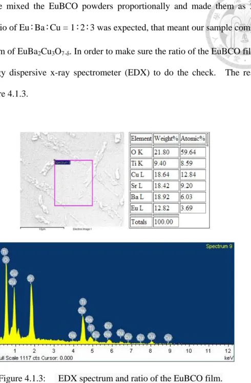
Because we mixed the EuBCO powders proportionally and made them as 2-inch targets, the ratio of Eu:Ba:Cu = 1:2:3 was expected, that meant our sample compound was in the form of EuBa2Cu3O7-δ. In order to make sure the ratio of the EuBCO film, we used an energy dispersive x-ray spectrometer (EDX) to do the check. The result is shown in figure 4.1.3.
Figure 4.1.3: EDX spectrum and ratio of the EuBCO film.
We can see that the ratio of Eu and Ba is close to the expectation value, but the proportion of Cu is excess about 3%. The EuBCO films were grown on the SrTiO3, so we can see that a part of elements are Sr and Ti.
The result from X-ray diffraction analysis for the EuBCO film is shown in figure 4.1.4. The distinguishable peaks indicate that our films are monocrystalline.
5 10 15 20 25 30 35 40 45 50 55 60 65 70 75 80 0
10000 20000 30000 40000 50000 60000 70000
(007) STO(002)
(009) (005)
(003)
(001)
Intensity (a.u.)
2deg
Figure 4.1.4: The XRD diagram of the EuBCO film.
The best Tc of the EuBCO film we’d fabricated is shown in figure 4.1.5, which is close to the result represented by P. H. Hor et al. in 1987 [2]. The R-T curve shows the zero resistance of the EuBCO film when the temperature is below Tc. The optimum sputtering conditions of the EuBCO film is P = 350 mTorr (Ar:O2 = 9:1) and 58OP (output power) which is about T = 700oC. The resultant superconducting transition temperature for the optimum deposition condition is about 90K.
0 20 40 60 80 100 120 140 160 180 200 220 240 260 280 300 0.0
0.1 0.2 0.3 0.4 0.5 0.6 0.7 0.8 0.9 1.0
R/R 0
T(K) EuBCO
88 89 90 91 92 93
0.0 0.1 0.2 0.3
R/R0
T(K)
Figure 4.1.5: The R-T diagram of the EuBCO film.
The magnetization-temperature (M-T) curves show the characteristics of zero-field cooling (ZFC) and field cooling (FC) for the EuBCO film. We can see the transition temperature of the EuBCO film is about 90K. The magnetization-temperature (M-T) curves shown in figure 4.1.6 indicate that our EuBCO film has the characteristics of type II superconductor.
75 80 85 90 95 100 105
-8.0x10⁻⁴ -7.0x10⁻⁴ -6.0x10⁻⁴ -5.0x10⁻⁴ -4.0x10⁻⁴ -3.0x10⁻⁴ -2.0x10⁻⁴ -1.0x10⁻⁴ 0.0 1.0x10⁻⁴
m (emu)
T (K) ZFC
FC H = 20 Oe
89.0 89.5 90.0 90.5 91.0 91.5 92.0 92.5 93.0 -1.0x10⁻⁴
-8.0x10⁻⁵ -6.0x10⁻⁵ -4.0x10⁻⁵ -2.0x10⁻⁵ 0.0
m (emu)
T (K)
Figure 4.1.6: The M-T diagram of the EuBCO film.
The following are the temperature dependence of ρ(T) in various magnetic fields for H∥(001) and H⊥(001). H∥(001) means the fields are parallel to the c-axis, and H⊥(001) means the fields are perpendicular to the c-axis. We can see the larger the applied magnetic field, the smaller the corresponding Tc, the tendencies are alike both in H∥(001) or H⊥(001).
In figure 4.1.6(a) and (b), we show the resistivities as a function of temperature for EuBCO in magnetic fields of 0, 0.25, 0.5, 1, 3 and 6 Tesla parallel and perpendicular to crystal c-axis, respectively. The resistive transition becomes broader in the fields parallel to the c-axis compared with the data obtained with the fields perpendicular to the c-axis. The result indicates the anisotropic properties of the EuBCO film
68 70 72 74 76 78 80 82 84 86 88 90 92 94 0.00
0.05 0.10 0.15
0.20 H=6T
3T 1T 0.5T 0.25T 0T
(m cm)
T(K)
H(001)
(a)
74 76 78 80 82 84 86 88 90 92 94 0.00
0.05 0.10 0.15 0.20
(m cm)
T (K)
H=6T 3T 1T 0.5T 0.25T 0T
H(001)
(b)
Figure 4.1.7: Temperature dependence of the resistivity ρ(T) of EuBCO film for (a) H∥(001) (b) H⊥(001) in the magnetic field up to 6 Tesla.
The upper critical fields Hc2 are defined by ten percent of resistivity corresponding to the Tc,onset from figure 4.1.6(a) (b). In order to determine Hc2(0) value, we applied Ginzburg – Landau (GL) theory [3]. The GL equation is
where is the reduced temperature [4].
Therefore, Hc2(0)∥(001) = 41.185 Tesla and Hc2(0)⊥(001) = 122.16 Tesla.
The anisotropy of the upper critical field:
γ The slopes are different from both field directions shown in figure 4.1.7.
72 74 76 78 80 82 84 86
0 1 2 3 4 5 6
HC2 (T)
T(K)
H(001) H(001)
Figure 4.1.8: Temperature dependence of the upper critical field Hc2(T) for both field directions.
According to Anderson and Kim’s flux creep model [5, 6]:
so the relation of lnρ - 1/T can be described as
where is the temperature independent constant and U0 is the apparent activated.
U(T, H) tends to to zero just above the onset of Tc because the superconductivity will vanish when temperature is above the onset of Tc. Then U0 can be obtained from the slope of the linear part of the lnρ − 1/T plot as shown in figure 4.1.8.
0.0110 0.0115 0.0120 0.0125 0.0130 0.0135 0.0140 0.0145 -17
-16 -15 -14 -13 -12 -11 -10 -9 -8 -7 -6
(a) -5
H(001)
ln[ xx( cm)]
1/T(1/K)
H=6T 3T 1T 0.5T 0.25T 0T
0.0115 0.0120 0.0125 0.0130 0.0135 0.0140 -17
-16 -15 -14 -13 -12 -11 -10 -9 -8 -7 -6
(b)
H=6T 3T 1T 0.5T 0.25T 0T H(001)
ln xx( cm)]
1/T (1/K)
Figure 4.1.9: lnρ(T,H) vs 1/T in various fields for (a) H∥(001) and (b) H⊥(001).
The U0-H relation shown in figure 4.1.9 can be obtained from figure 4.1.8. We can see that the apparent activated U0(K) decreases with the increase of applied magnetic field both in H∥(001) and H⊥(001). The temperature scale for the activation energy can be normalized as Uo/T.
1 10
2000 4000 6000 8000 10000 12000 14000
H(001) H(001) U 0(K)
H(T)
Figure 4.1.10: Field dependence of U0(K).
4.2 The SNS structure
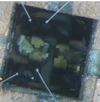
According to the previous statements in chapter 3, we fabricated the SNS structure with the technique of Focused Ion Beam (FIB). Then we also checked the two electrodes whether those were disconnected before we coated the gold on the part of cutting regions. Then we annealed the SNS structure because of the importance of annealing. The optical image of the sample is shown in figure 4.2.1.
The experiment was carried out in a cryostat system. The SNS structure was measured by Keithley 236 and Keithley 2000 multi-meter with four-terminal techniques.
The R-T data of the SNS structure was recorded automatically by a computer equipped with a Labview program.
Figure 4.2.1: The optical image of the SNS structure. (This device was made by Lung-Yi Huang and Yu-Feng Huang.)
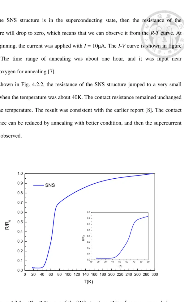
If the SNS structure is in the superconducting state, then the resistance of the structure will drop to zero, which means that we can observe it from the R-T curve. At the beginning, the current was applied with I = 10μA. The I-V curve is shown in figure 4.2.2. The time range of annealing was about one hour, and it was input near 1Atm-oxygen for annealing [7].
As shown in Fig. 4.2.2, the resistance of the SNS structure jumped to a very small value when the temperature was about 40K. The contact resistance remained unchanged with the temperature. The result was consistent with the earlier report [8]. The contact resistance can be reduced by annealing with better condition, and then the supercurrent can be observed.
0 20 40 60 80 100 120 140 160 180 200 220 240 260 280 300 0.0
0.1 0.2 0.3 0.4 0.5 0.6 0.7 0.8 0.9 1.0
R/R 0
T(K) SNS
10 20 30 40 50 60 70 80 90
0.0 0.1 0.2 0.3 0.4 0.5 0.6 0.7 0.8
R/R0
T(K)
Figure 4.2.2: The R-T curve of the SNS structure. (This diagram was made by
4.3 The SGS structure
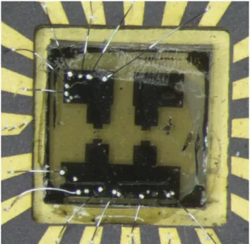
We fabricated new superconducting electrodes with the gap of about 100 nm by Focused Ion Beam (FIB). The graphene was transferred on the bridge between two superconducting electrodes shown in figure 4.3.1. Because the graphene is transparent and hard to be seen, therefore we measured the resistance of the SGS structure at room temperature for checking whether we make it successfully.
Figure 4.3.1: The optical image of the SGS structure. (This device was made by Lung-Yi Huang and Yu-Feng Huang.)
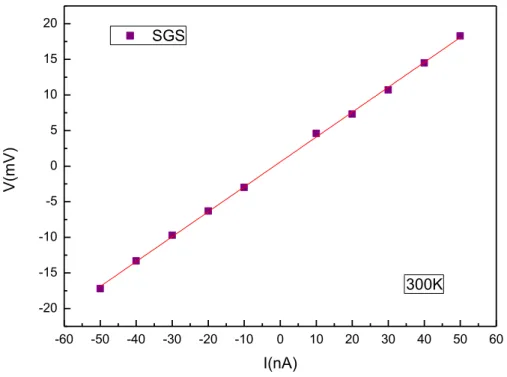
In order to identify the Ohmic region, we measure the I-V relation of the SGS structure before we cool down the device. The current-voltage (I-V) curve shown in figure 4.3.2 is linear at room temperature.
-60 -50 -40 -30 -20 -10 0 10 20 30 40 50 60 -20
-15 -10 -5 0 5 10 15 20
300K
V(mV)
I(nA) SGS
Figure 4.3.2: The current-voltage (I-V) curve of the SGS structure at 300K. (This diagram was made by Lung-Yi Huang and Yu-Feng Huang.)
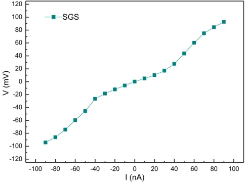
The SGS structure was measured by Keithley 236 and Keithley 2000 multi-meter with four-terminal technique. The I-V curve shown in the figure 4.3.3 was about 10K.
We found that the I-V curve at 10K is not linear from -90nA to 90nA. The slope changed from -50nA and 50nA. Although the intermediate part of the I-V curve is not very flat, the variation of resistance is clear. There is one reason led this happen. That is, there were only few amounts of cooper pairs passing through the graphene which connects two superconducting electrodes. On the other hand, the contact resistance is a big problem for this kind of structure. The contact resistance is too large to see the supercurrent, so the typical I-V curve of Josephson junction is not represented.
-100 -80 -60 -40 -20 0 20 40 60 80 100
-120 -100 -80 -60 -40 -20 0 20 40 60 80 100 120
V (mV)
I (nA) SGS
Figure 4.3.3: The current-voltage (I-V) curve of the SGS structure about 10K. (This diagram was made by Lung-Yi Huang and Yu-Feng Huang.)
The large contact resistance obstructs the characteristic that we want to observe. In order to check whether the reason is only from the large contact resistance, we measured the R-T of superconducting electrodes. It is shown in figure 4.3.4. The characteristic of superconductor still exists.
0 25 50 75 100 125 150 175 200 225 250 275 300 0
1 2 3 4
R ()
T (K) EuBCO electrodes
30 40 50 60 70 80
0.0 0.5 1.0 1.5 2.0 2.5
R ()
T (K)
Figure 4.3.4: The R-T curve of the superconducting electrodes. (This diagram was made by Lung-Yi Huang and Yu-Feng Huang.)
References
[1] P. Boochand, R. N. Enzweiler, Ivan Zitkovsky, Solid State Communications, 63, 521 (1987).
[2] P. H. Hor, R. L. Meng, Y. Q. Wang, L. Gao, Z. J. Huang, J. Bechtold, K. Forster, and C. W. Chu, Physical Review Letters, 58, 1891 (1987)
[3] V. L. Ginzburg and L. D. Lndau, J. Exp. Theor. Phys. , U. S. S. R. , 20, 1064 (1950)
[4] X. Wang, S. R. Ghorbani, G. Peleckis, and S. Dou, Adv. Mater., 21, 236 (2009) [5] P. W Anderson, Physical Review Letters, 9, 309 (1962).
[6] Y. B. Kim, C. F. Hempstead and A. R. Stranad, Phys. Rev. 131, 2486 (1963).
[7] B. Ghyselen, R. Cabanel, S. Tyc, D.G. Crété, Z.H. Barber, J.E. Evetts, G. Ben Assayag, J. Gierak and A. Schuhl, Physica C 198, 215 (1992)
Chapter 5 Perspective
There are still problems we need to solve: The large contact resistance of the SGS structure and the quality of the EuBCO films.
The Tc of our EuBCO film is about 90K that is close to the result of paper [1].
Although the higher Tc is the indicator of the sample quality, but we didn’t reduce the roughness successfully, the surface of our EuBCO film shown in figure 5.1 is still very rough. One can expect that a flatter surface of EuBCO would be helpful to our measurment. Nevertheless, we can not only attribute the large contact resistance of the SGS structure to the roughness of our EuBCO films.
Second, we can find the better condition of annealing the SGS structure, so that it can improve the interface between graphene and superconducting electrodes, just like the SNS structure we fabricated.
Third, we can put the gate on the SGS structure in the future, and then we can tune the gate voltage to enlarge the carrier density. We may see the supercurrent passing through the device because of the increment of carrier density [2].
Due to the different physical properties of graphene and superconductor, the interfaces should be improved. The improvement of interface between the graphene/superconductor is a challenge. If the problem is solved, the new physics may emerge.
References
[1] P. Boochand, R. N. Enzweiler, Ivan Zitkovsky, Solid State Communications, 63, 521 (1987).
[2] T. Sato, T. Moriki, S. Tanaka, A. Kanda, H. Goto, H. Miyazaki, S. Odaka, Y. Ootuka, K. Tsukagoshi, Y. Aoyagi, Physica E, 40, 1495 (2008)
![Figure 2.5.1: Resistively Capacitance Shunted Junction [10].](https://thumb-ap.123doks.com/thumbv2/9libinfo/9603070.629481/26.892.165.777.106.533/figure-resistively-capacitance-shunted-junction.webp)
![Figure 4.1.1: The crystal structure of EuBCO. The layers of Cu (black) and O (white) normal to the c-axis, here along the horizontal [1]](https://thumb-ap.123doks.com/thumbv2/9libinfo/9603070.629481/40.892.153.794.126.360/figure-crystal-structure-eubco-layers-black-normal-horizontal.webp)