國立台灣大學電機工程學研究所 碩士學位論文
D
EPARTMENT OFE
LECTRICALE
NGINEERINGC
OLLEGE OFE
LECTRICALE
NGINEERING ANDC
OMPUTERS
CIENCEN
ATIONALT
AIWANU
NIVERSITYM
ASTERT
HESIS根據蒙地卡羅法之電子軌跡模擬與應用於多電子束微影之 電子束位置感測器設計
MONTE CARLO SIMULATION OF ELECTRON TRAJECTORY AND
DESIGN OF AN ELECTRON BEAM POSITION MONITOR SYSTEM
FOR MULTIPLE ELECTRON BEAM DIRECT-WRITE LITHOGRAPHY
范期翔 Chi-Hsiang Fan
指導教授:蔡坤諭 博士 共同指導教授:陳永耀 博士
Advisor: Kuen-Yu Tsai, Ph.D.
Co-Advisor: Yung-Yaw Chen, Ph.D.
中華民國九十七年六月
Abstract
Electron beam lithography is one of the promising candidates for next generation lithography because of the ultra-high resolution and the property of need no mask. In order to improve the problem of slow throughput, miniature electrostatic elements are widely utilized in order to drive large amount of beams at one time.
The electron beam drift problem becomes series and can not be neglected in a multiple electron beam lithography system. Current single electron beam lithography systems utilize periodic recalibration with reference markers on the wafer to achieve beam placement accuracy. But the technique becomes impractical with multiple beams.
In this thesis, architecture of beam position monitor system for multiple electron beam lithography is proposed. It consists of an array of electron detector placed above the wafer, which can detect the distribution of the backscattered electrons for each electron beam. The beam drifts and backscattered electrons distribution relation is simulated by Monte Carlo method using in-house MATLAB code. From the Monte Carlo electron trajectories simulation, it is believed that the change of backscattered electron distribution result from the electron beam drifts can be detected by the detector array. The beam drift can be calculated by using the detector output signals.
Statement of Contributions
General Contributions
The following items, although not my original contributions, are considered substantial as follow.
1. Deliver a Monte Carlo electron trajectory simulator.
2. Deliver a customized Monte Carlo simulator that can provide complete information of each backscattered electron, which is useful for future research on detectors, lens, and processes
Original Contributions
My original contributions are as follow.
1. Initial performance assessment of a preliminary beam monitor system ((joint work with Y. D. Chiang)
2. Propose a new detector architecture for beam drift detection and focus detection for multiple electron beam direct write (joint work with Prof. Y. Y. Chen, K. Y.
Tsai, and J. Y. Yen)
誌謝 誌謝 誌謝誌謝
碩士班兩年的時光中,首先要感謝指導教授蔡坤諭老師對我的栽培,在研究過程 中給我偌大的發揮空間,不分晝夜的給予我指導,提供我豐沛的研究資源,不間 斷地與我討論研究到最後一刻,並不時在處事與工作上給我建議、鼓勵。接下來 要感謝我的共同指導教授陳永耀老師,指引我研究大方向,一步步引導我深入思 考問題,在我的研究上給予莫大的幫助。感謝 e-beam 團隊顏家鈺老師和李佳翰 老師對我的照顧與指導。感謝艮軒學長對我的照顧,不吝惜的分享研究經驗和專 業知識,我的室友兼戰友啟智,在壓力最大的時候互相勉勵,每天陪我宵夜,俊 宏、水源、壹倫、沛霖、孟福、育諄學長對我的關心與支持,兩年來互相扶持的 伙伴們昭文、信全、信宏、偉志、宇鋕,感謝大家帶給我兩年收穫豐盛的碩士生 活。感謝父母和哥哥,成為在生活上最大的支柱;感謝樂團的伙伴們,為我的碩 士生活增添許多色彩。最後要感謝台大電機系,給我最頂尖的學習環境和資源。
范期翔
Table of Contents
Abstract I
Statement of Contributions II
誌謝 誌謝 誌謝
誌謝 III
Table of Contents IV
List of Figures VI
List of Table VIII
Chapter 1 Introduction 1
1.1 Microlithography... 1 1.2 Electron Beam Lithography ... 2 1.3 Multiple E-beam Lithography ... 3
Chapter 2 Electron Detector 5
2.1 Electron-Solid Interaction ... 5 2.2 Electron Detector in an SEM... 6 2.2.1 Secondary Electron Detector (Everhard-Thornley detector) 6
2.2.2 Backscattered Electron Detector 6
Chapter 3 Beam Drift Compensation 8
3.1 Beam Drift Error in Electron Beam Lithography... 8 3.2 Electron Beam Calibration in SEM... 8 3.3 Detector Array Architecture Design for Multiple Electron Beam Lithography System... 9
Chapter 4 Monte Carlo Simulation 11
4.1 Theory of Electron Trajectories Simulation by Monte Carlo Method ... 12 4.2 Electron Trajectory Simulation ... 13
4.2.1 Program flow 13 4.2.2 Calculation of Mott Scattering Cross Section 16
4.2.3 Calculation of Electron Direction 19
4.2.4 Distance between Two Collisions 23
4.2.5 Energy Loss 23
4.2.6 Secondary Electrons 24
4.3 Gaussian Beam ... 26
4.4 Simulation Results... 28
4.4.1 Electron trajectories 28 4.4.2 Energy distribution 31 Chapter 5 Backscattered Electrons 33 5.1 Backscattering coefficient ... 33
5.2 Energy distribution of backscattered electrons ... 36
5.3 Multi-layer... 37
Chapter 6 Design and Optimization of the Detector Array 40 6.1 Collection Efficiency... 41
6.1.1 Working Distance 41 6.2 Beam Oblique... 43
Chapter 7 Silicon Photodiode & Application to MPML2 45 7.1 Response of silicon photodiode... 45
7.2 MPML2 ... 47
7.3 Fabrication of detector array for MPML2... 49
7.4 Simulation of the response of detector array in MPML2... 52
Chapter 8 Conclusions and Future Work 54
Bibliography 55
List of Figures
Figure 2.1: The International Technology Roadmap for Semiconductor ...2
Figure 2.2: Multiple e-beam lithographic system by Seoul University and MAPPER .4 Figure 2.3: Concepts of arrayed microcolumn lithography by Etec Systems, Inc. ...4
Figure 3.1: Electron-solid interaction ...6
Figure 4.1: The SEM calibration specimen. ...9
Figure 4.2: Concept of beam position monitor system ...10
Figure 5.1: Game of battleship and collision of electron...11
Figure 5.2: Elastic collision and energy loss ...12
Figure 5.3: Monte Carlo simulation program flow...13
Figure 5.8: Idea of Monte Carlo electron trajectory simulation ...14
Figure 5.4: Monte Carlo electron trajectory simulation...16
Figure 5.5: Differential Mott cross section of silicon as the function of polar angle. .18 Figure 5.6: Polar angle of silicon as the function of random number...20
Figure 5.7: New direction of an electron after a collision in Monte Carlo simulation 22 Figure 5.9: Schematic illustration of the electron energy vs. path length in the hybrid model...26
Figure 5.10: 2D Gaussian distribution...27
Figure 5.11: landing positions...28
Figure 5.12: Monte Carlo simulation result of 300 eV electron energy ...29
Figure 5.13: Monte Carlo simulation result of 500 eV electron energy. ...29
Figure 5.14: Monte Carlo simulation result of 1000 eV electron energy. ...30
Figure 5.15: Monte Carlo simulation result of 2000 eV electron energy ...30
Figure 6.1: The experiment arrangement proposed by Gomati for backscattering coefficient. ...34
Figure 6.2: Experiments and Monte Carlo simulations of backscattering coefficient.35 Figure 6.3: Backscattered electron energy distribution ...36
Figure 6.4: Backscattered electron energy distributions for 10 nm HSQ on silicon ...38
Figure 6.5: Backscattered electron energy distributions for 20 nm HSQ on silicon ...38
Figure 6.6: Backscattered electron energy distributions for 30 nm HSQ on silicon ...39
Figure 7.1: The preliminary design of the detector architecture of beam position monitor system for multiple electron beam lithography system...40
Figure 7.2: Working distance...42
Figure 7.3: Collection efficiency as a function of working distance. ...42
Figure 7.4: The scheme of the simulation for electron beam drifting error...43
Figure 7.5: Variation of the detectors output ...44
Figure 8.1: Schematic of 100% internal quantum efficiency silicon photodiode...46
Figure 8.2: Photodiode responsivity from 0.2 to 40keV electrons ...47
Figure 8.3: Schematics of MPML2...48
Figure 8.4: Quadrant section view illustrating the PIN detector structure ...49
Figure 8.5: A schematic representation of the process flow...51
Figure 8.6: PIN electron detector array...52
Figure 8.7: Simulation of the detectors signal variation ...53
List of Table
Table 5.1: The 26 energies at which the Mott cross section has been computed in the work of Czyzewski et al. ...18 Table 5.2: The 96 values of differential Mott cross section in each block. ...20 Table 5.3: Variables used to interpolating polar angle ...21 Table 6.1: Mean atomic number (Zav) and mean ionization potential for PMMA, ZEP520A, and HSQ...37
Chapter 1 Introduction
1.1 Microlithography
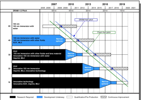
Microlithography, a technique that transfers the desired pattern from the mask to the wafer, is one of the most important processes in integrated circuit fabrication. At the present day, optical lithography is the mainstream of all microlithography techniques. The desired pattern is defined on mask, and the image of mask is then projected onto the wafer. The photosensitive material, called photo resist, coated on the wafer brings complicated chemical reaction after exposed under the ultra-violet. A chain of chemical process such as etching and deposit build the micro structures on the exposed area. After more than twenty rounds of these processes, the integrated circuit is built on the chip. Since microlithography defines the desire pattern for each layers of integrated circuit, the precision of microlithography is the most critical dominant of semiconductor manufacturing technology. At present, optical lithography uses 193 nm deep ultra-violet to project wafers, and under the support of water immersion technique, the resolution achieves 45 nm in half-pitch.
According to the International Technology Roadmap for Semiconductor (ITRS), the resolution in half-pitch of semiconductor manufacturing technology need to reaches 32 nm in the year 2013. The resolution of photolithography is restricted to the effect of diffraction. Many next-generation lithography techniques are proposed to achieve the target.
DRAM 1/2 Pitch 65nm 45nm 32nm 22nm 16nm
2007 2010 2013 2016 2019
2006 2008 2009 2011 2012 2014 2015 2017 2018 2020 2021
2005
i
Development Underway Qualification/Pre-Production Continuous Improvement Research Required
This legend indicates the time during which research, development, and qualification/pre-production should be taking place for the solution.
EUV
193 nm immersion with other fluids and lens material Innovative 193 nm immersion with water Imprint, ML2
EUV
Innovative 193 nm immersion Imprint, ML2, innovative technology
Innovative technology Innovative EUV, imprint, ML2 193 nm immersion with water 193 nm immersion with other fluids EUV, ML2
Narrow options
Narrow options Narrow options
Narrow options
Narrow options 193 nm
193 nm immersion with water
65
45
32
22
16
DRAM Half-pitch
Flash Half-pitch
Figure 1.1: The International Technology Roadmap for Semiconductor
1.2 Electron Beam Lithography
The first electron beam lithography system, which is based on the scanning electron microscope, is developed in late 1960s. The processes of electron beam lithography are similar to the optical lithography except the ultra-violet light that expose to the wafer is replaced by the electron beam and the photo resist that coated on the wafer is replaced by material that can react to the electrons. Since the wavelength of the electron beam is extremely small, electron beam lithography can achieve sub-10 nm resolution, theoretically.
An advantage of electron beam lithography is that no mask is needed. The desire pattern is directly written on the wafer. Just like using an extremely sharp pen to write
an imperceptible picture. Currently, electron beam lithography is often used to produce the mask that used in optical lithography. The reason that electron beam lithography is not commonly used in semiconductor manufacturing is that the throughput is not fast enough to handle the massive production industry. It takes about one day to expose a 12 inches size wafer by using a single beam lithography system.
1.3 Multiple E-beam Lithography
Electron beam lithography is one of the promising candidates for next generation lithography because of the ultra-high resolution and the property of need no mask.
Multiple electron beam lithography has become a popular research topic in order to solve the problem of slow throughput. By using the MEMS processes, the dimension of lenses and other structures needed in electron beam lithography system can be shrunk to sub-millimeter. A large amount of electron beams can be driven at the same time and expose on the same wafer so that the throughput is improved. Though the improved throughput claimed in variety of multiple e-beam systems are not capable to compete with optical lithography, the features of maskless manufacturing and high resolution are still attractive to the semiconductor industry.
Figure 1.2: Multiple e-beam lithographic system by Seoul University (left) and MAPPER (right)
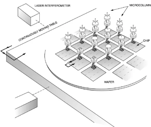
Figure 1.3: Concepts of arrayed microcolumn lithography by Etec Systems, Inc.
Chapter 2 Electron Detector
Scanning electron microscope (SEM) is used to discover the vision under nanometre scale for the past seventy years. The first SEM image was obtained by Max Knoll in 1935.
When the electrons strike the specimen, complicated energy transfer between electrons and molecular of the sample carry out signals such as backscattered electrons, secondary electrons, X-ray, light…etc. These signals respond the surface topology and the chemical composition of the specimen. The electron beam scans an area in a regular pattern, and with proper detectors to detect the signals, the information of the area on the specimen can be known.
2.1 Electron-Solid Interaction
Electron signals represent much useful information. Understanding the electron-solid interaction is an important subject.
When the electrons strike the specimen, some of the electrons will be attracted to the positive nucleus and change moving direction in a large angle. If these electrons then depart the specimen and bring high energy originating from the electron beam, they are called “backscattered electrons.” Others electrons absorb their energy in the specimen, and excite the valence electrons form the specimen atomic. These excited electrons are mostly originated within a few nanometers from the surface and carry low energy (<50 eV). They are called “secondary electrons.”
Figure 2.1: Electron-solid interaction
2.2 Electron Detector in an SEM
2.2.1 Secondary Electron Detector (Everhard-Thornley detector)
Due to the low energy of these secondary electrons, they are detected by an Everhard-Thornley detector which is a scintillator-photomultiplier. With a collector that produces an electrical field, the laggardly secondary electrons are attracted to the Everhard-Thornley detector so the collection is more efficiency. The scintillator-photomultiplier amplifies the electron signal by using high voltage to accelerate these electrons. The number of secondary electrons accrue, is related to the specimen surface. By analyze the secondary electrons signal, the topology of the surface can be known.
2.2.2 Backscattered Electron Detector
Backscattered electrons consist of high-energy electrons originating in the electron beam. The collection efficiency is difficult to increase by adding an electrical
field that changes the electrons’ trajectory. The backscattered electrons detector is in a shape like “doughnut.” The electron beam pass through the hole of the “doughnut,”
and the electrons scatter back are captured by the rounded detective area.
The number of backscattered electrons accrue is correlated with the atomic number. So the backscattered electron image is related to the atomic number of the chemical composition of the specimen.
Chapter 3 Beam Drift Compensation
3.1 Beam Drift Error in Electron Beam Lithography
Multiple electron beams lithography system offer the promise of high resolution due to the lack of the diffraction effects which restrict the optical lithography systems.
However, the multiple electron beam lithography suffers from degradation due to the charging effects and some unanticipated magnetic field.
There are two aspects of charging effects[5] in an electron beam lithography system, the global effect and the stochastic effect. The global charge effect results from the mutual repulsion of electron beams. The electron beams will tend to shift outward and strike the undesired position. The stochastic charge effect results from the collision of individual electrons in the beam. This variation causes a blur in the electron image.
The unanticipated magnetic field might be caused by many reasons. The electric device in the chamber and accumulation of electrons on the specimen may produce some magnetic field. These magnetic fields also causes the electron beams to drift, and these drifting error will increase as the operation time grows.
3.2 Electron Beam Calibration in SEM
Currently, the scanning electron microscope utilizes periodic recalibration with reference markers on a test specimen. There are millions gold squares of 1 µm size on
Figure 3.1: The SEM calibration specimen.
The white area is gold and the dark area is silicon.
silicon. These gold squares are arranged like a checkerboard with interval of 1 µm.
When the electron beam scans on the calibration specimen, the backscattered electron signals vary due to the different elements. The gold pattern on the specimen is believed to have an accuracy of 10 nm. By the variation of the electron signal, the scanning distance and direction is known, and electron beam position can be corrected.
3.3 Detector Array Architecture Design for Multiple Electron Beam Lithography System
The calibration technique used in the scanning electron microscope becomes
Figure 3.2: Concept of beam position monitor system
impractical with the multiple electron beam lithography system. It is impossible to calibrate each electron beam on the calibration specimen.
Architecture of beam position monitor system for multiple electron beam lithography is proposed in this thesis. It consists of an array of electron detector placed above the wafer, which can detect the distribution of the backscattered electrons for each electron beam. The backscattered electrons distribution is related to the beam position. As the beam drift to one side, one of the detectors in the detector array may generate an ascending signal, and one of the other may generate a descending signal. By comparison the magnitudes of each signal generate from the detectors, the beam position can be measured.
Since the beam position monitor system is based on the detection of backscattered electron, understanding the behaviour of backscattered electrons is important. A Monte Carlo electron trajectories simulation will be discussed in the next chapter.
Chapter 4 Monte Carlo Simulation
A Monte Carlo method is a computational algorithm that relies on repeated computation and pseudo-random numbers to compute the result. It is often used on physics simulation. The simulation of electron trajectories in solids is one of the applications.
The Monte Carlo method can illustrated as a game of “battleship.” First, a shot point is selected. If the target is hit, there will be two choices for next shot by guessing the shape of the battleship. Finally, the next shot point is generated. The simulation of electron trajectories in solids can be explained in the same way. The electron changes its moving direction because of collision to another charged particle.
Figure 4.1: Game of battleship and collision of electron
The new direction is decided by algorithms and pseudo-random numbers. Repeat the procedure and calculate the energy loss until the electron lose all the energy and stop, the simulation is complete.
4.1 Theory of Electron Trajectories Simulation by Monte Carlo Method
The electron trajectories simulation by Monte Carlo method consists of two major models. The first one is the elastic collision, and the other is the energy loss.
The elastic collision can be seen as the electron attracted by the positive charged nucleus. The electron changes its moving direction in big angle. The energy loss in the collision is small and can be neglected.
All the physics that cause the electron to lose energy in the solid are considered in the energy loss model included the phenomena of the generation of secondary electrons. The change of the electron moving direction result from these phenomena is small and can be neglect in the simulation.
+ + ++
-
-
Elastic Collision
+ + ++
- - -
Energy Loss
Figure 4.2: Elastic collision and energy loss
4.2 Electron Trajectory Simulation
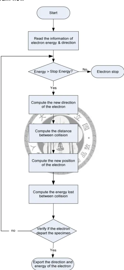
4.2.1 Program flow
Figure 4.3: Monte Carlo simulation program flow
The first step of running the Monte Carlo simulation program is to read the information including the energy, the moving direction and the landing position of the incident electrons. Then the program will verify that if the electron has enough energy to occur an event of collision. If the energy of the electron is less than the stop energy (50 eV), the program will stop simulate the trajectory of the electron. The choice of the 50 eV value is purely arbitrary and historical. As the backscattered electrons are emphasized in this thesis, the number of the backscattered electrons, which have energy lower than 50 eV, is comparison to be very small in real situation. These low energy electrons can be safely neglected in simulation.
The new direction is then computed by the polar angle θ, and azimuth angle ϕ. The polar angle and the azimuth angle are decided by Monte Carlo method which involves the random number and the Mott scattering cross section.
Figure 4.4: Idea of Monte Carlo electron trajectory simulation
The distance L to the next collision point is also decided by Monte Carlo method involving random number and electron mean free path. With the new direction and the distance L, the new possible collision point can be evaluated. A continuous slowing down approximation is applied on the energy loss model. The energy loss between two collision point and the energy of the electron at the next collision point can be calculated.
Then the Monte Carlo simulation program will check the electron position. If the electron remains in the area that is defined to be the specimen, the new moving direction and new electron energy is set to be the initial condition and checked if the electron has enough energy to occur a collision. These procedures are repeated until the electron energy is low (<50 eV). If the electron leaves the area that is defined to be the specimen, the electron is defined as a “backscattered electron” and continues moving in a straight line with the direction and energy when it departs the specimen.
The information of each backscattered electrons is stored in a table and is available for the design of detectors.
-50 -40 -30 -20 -10 0 10 20 30 40 50 -40 -50
-20 -30 -10 10 0 20 40 30 50 -20 -15 -10 -5 0 5 10
X (nm) Y (nm)
Z (nm)
Silicon
Indicent Energy 400eV 20 trajectories
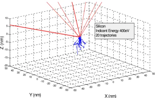
Figure 4.5: Monte Carlo electron trajectory simulation
The area under the plane Z=0 is defined to be the silicon substrate. 20 trajectories were simulated in this figure. The blue lines represent the electron trajectories under the specimen. The red lines represent the backscattered electron trajectories.
4.2.2 Calculation of Mott Scattering Cross Section
Calculate Mott scattering cross section is the most important part for simulation of elastic scattering of the Monte Carlo modelling technique. The elastic scattering can be seen as the electron attracted by the positive charged nucleus.
The Dirac equation should be used in calculations to determine the electron scattering in the relativistic case. The reduced scattering wave functions are two sets of two coupled first order differential equations
( ) ( ) ( ) ( ) ( ) ( ) ( ) ( ) ( )
( )
[ 1] 1 0
[ 1] 1 0
±
± ±
±
± ±
− + + + + =
− − − + + − =
n
n n
n
n n
dG r k
W V r F r G r
dr r
dF r k
W V r G r F r
dr r
(4.1)
where W is the total energy of the incident electron. The sign “+” applies to the “spin
up” case, the sign “-” applies to the “spin down” case, i.e.
( 1) 1
2 1 2
denotes ,
denotes ,
+ = − + = +
− = = −
k n j n
k n j n
(4.2)
where j is the total angular momentum of the nth partial wave. The requires asymptotic solution for large r, where V r( ) 0≈ is
( ) ( ) cosη ( )sinη
± = ±− ±
n n n n n
G r J Kr T Kr (4.3)
where J Krn( ) and T Krn( ) are Bessel and Neumann functions, respectively,
2 = 2−1
K W , and the ηn are the Dirac phase shifts. Condition (4.4) directly leads to following equations for scattering factors:
( ) ( ) ( )
{ }
( ) ( )
1 1
0
1 1
( ) 1 1 exp 2 1 exp 2 1 (cos )
2
( ) 1 exp 2 exp 2 (cos )
2
θ η η θ
θ η η θ
∞
− − − −
=
∞
− −
=
= + − + −
= − + ′
∑
∑
n n n
n
n n n
n
f n i n i P
iK
g i i P
iK
(4.4)
and the elastic differential scattering cross section
( )
2 2
2 2
σ ∗ ∗ − ∗ −ϕ
= + + −
Ω +
d AB e i
f g fg f g
d A B (4.5)
where i= −( 1)1 2 , Pn and Pn′ are the ordinary and the associated Legendre polynomials, respectively, A, B, and ϕ describe the direction and degree of spin polarization of the incoming electron, θ is the scattering angle.
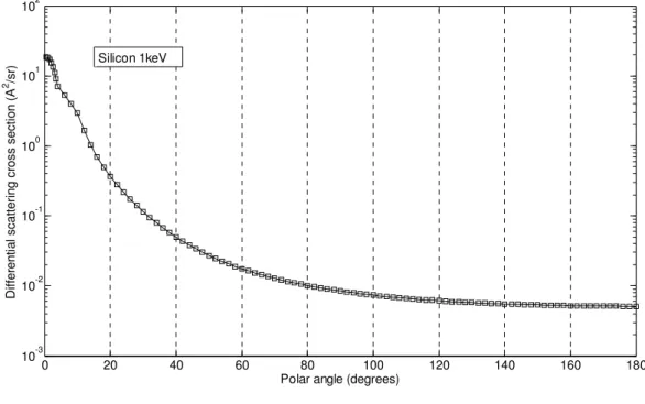
The differential Mott cross sections for each element of the periodic table were computed and published in the work of Czyzewski[6] et al. There are 26 blocks of data
0 20 40 60 80 100 120 140 160 180 10-3
10-2 10-1 100 101 102
Polar angle (degrees) Differential scattering cross section (A2/sr) Silicon 1keV
Figure 4.6: Differential Mott cross section of silicon as the function of polar angle.
for each element. Each block represents different energies. Each block has 96 values of differential Mott cross section for corresponding polar angles.
Table 4.1: The 26 energies at which the Mott cross section has been computed in the work of Czyzewski et al.
Energy(eV) Number of blocks
20 1
50 1
75 1
100 to 1000 by step of 100 eV 10
2000 to 10000 by step of 1000 eV 9
20000 to 30000 by step of 5000 eV 4
Total 26
4.2.3 Calculation of Electron Direction
In the Monte Carlo simulation, the electron moving direction after a collision is decided by the value of polar angle θ, and azimuth angle ϕ.
The total elastic cross section is used to determine the polar angle θ. To compute the total elastic cross section σT, the differential cross section must be integrated using the following equation
2 0π σ sin
σ = π θ θ
∫ Ω
T
d d
d (4.6)
where θ is the polar angle and σ Ω d
d is the differential cross section. This equation is calculated by numerical integration by using the differential cross section data provided by Czyzewski et al.
For a given energy E which the value is not on the 26 tabulated energies, the total elastic cross section σT has to be calculated by interpolating. The first step is to find the nearest lower energy Emin and upper energy Emax in the 26 tabulated energies.
The total elastic cross section for Emin and Emax can be calculated using equation (4.6). Then the total elastic cross section σT( )E for energy E is
( ) ( ( ) ( ))
( ) ( ) σ σ
σ =σ + − × −
−
T T
T T
E Emin Emax Emin
E Emin
Emax Emin (4.7)
where σT(Emin) is the total elastic cross section for Emin and σT(Emax) is the total elastic cross section for Emax.
Table 4.2: The 96 values of differential Mott cross section in each block.
Polar angles (degrees) Number of values
0.5 to 4 by step of 0.5 degree 8
6 to 180 by step of 2 degree 88
Total 96
A probability of event is determined to compute θ. With a random number R1, distributed uniformly between 0 and 1, a value of polar angle θ is determined by using the following equation.
1 2 0θ σ sin
σ = π θ θ
∫ Ω
T
R d d
d (4.8)
By using numerical integration, the polar angle θ can be seemed as a function of R1. Because of that the differential Mott cross section are 96 discrete values, the polar angles θ are also 96 discrete values corresponding to different values of random number R1. As the random number R1 is selected, the polar angle θ is determined by
0 0.1 0.2 0.3 0.4 0.5 0.6 0.7 0.8 0.9 1
0 20 40 60 80 100 120 140 160 180
R1
Polar angle (degrees)
Silicon 1keV
Figure 4.7: Polar angle θ of silicon at 1keV as the function of random number R1.
Table 4.3: Variables used to interpolating polar angle polar angles
Emin E Emax
Rmax θEmin(Rmax) θEmax(Rmax)
R θEmin θE θEmax
R1
Rmin θEmin(Rmin) θEmax(Rmin)
interpolation. The first step of evaluating the polar angle θ for a specific energy E is to find the nearest lower energy Emin and upper energy Emax in the 26 tabulated energies. Establish a table of polar angle θ as a function of R1 using equation(4.8) for Emin. Then the program generate a random number R between 0 and 1 and find the
nearest lower value Rmin and upper Rmax in the 96 tabulated values that corresponding to the polar angles. The polar angle θEmin for energy Emin and random number R is determined by the equation
( ) ( ( ) ( ))
( ) θ θ
θ =θ + − × −
−
Emin Emin
Emin Emin
R Rmin Rmax Rmin
Rmin Rmax Rmin (4.9)
The polar angle θEmax for energy Emax is determined by the same way
( ) ( ( ) ( ))
( ) θ θ
θ =θ + − × −
−
Emax Emax
Emax Emax
R Rmin Rmax Rmin
Rmin Rmax Rmin (4.10)
Finally, the polar angle θE for energy “E” is computed by interpolating between
“Emax” and “Emin” using the following equation.
( ) (θ θ )
θ =θ + − × −
−
Emax Emin
E Emin
E Emin
Emax Emin (4.11)
The azimuth angle ϕ is uniformly distributed from 0 to 2π and is given by equation (4.12):
2 2
ϕ=R × π (4.12)
where R2 is another random number distributed uniformly from 0 to 1.
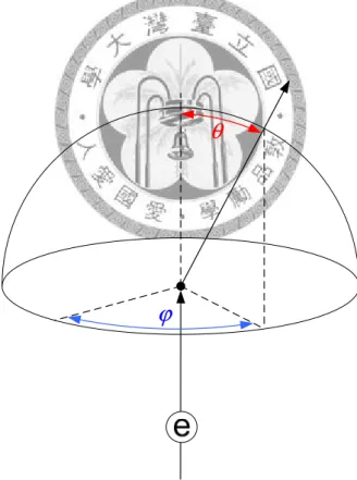
As the polar angle θ and the azimuth angle ϕ is decided, the new moving direction of the electron after an elastic collision event is defined by the geometric relationship in the spherical coordinate system shows in the Figure(4.8).
θ
ϕ
Figure 4.8: New direction of an electron after a collision in Monte Carlo simulation
4.2.4 Distance between Two Collisions
To determine the distance L between two collisions, the electron mean free path must be calculated first.
Electron mean free path λ describe the average distance travelled by an electron between two consecutive collisions. The electron mean free path λ is proportional to the inverse of the elastic cross section.
0 1
1 σ
λ ρ =
= ∑n i i
i i
N C
A (4.13)
where Ci, Ai are the weight fraction and atomic weight of element i. ρ is the density of the element and N0 is the Avogadro’s constant.
A probability of event is determined to compute λ. With a random number R3, distributed uniformly between 0 and 1, a value L is determined by using the following equation.
log( )3
λ
= −
L R (4.14)
4.2.5 Energy Loss
The effect of energy lost on electron deviation is neglected in the simulation. All the electron energy loss events are groups in a continuous slowing down approximation. With this assumption, the energy at position i is computed by the following equation:
1
= − + ×
i i
E E dE L
dS (4.15)
where Ei and Ei−1 are the respective energy at current and previous collision. dE dS
The Bethe-Bloch formula which was found by Hans Bethe in 1930 is used to describe the energy loss per distance traveled of electrons. The formula reads:
( )
2 2 2
2 2
2 2 2
0
2
4 ln
4 1
π β
β πε β β
= − × × − −
e e
m c
dE n e
dS m c J (4.16)
where β = v c and v is the velocity of the electron, c is the speed of light. e is the charge of the electron (–1.602176487×10⁻¹⁹ C). me is the rest mass of the electron. J is the mean ionization potential of the target. ε0 is the permittivity of free space (8.8541878176×10⁻¹² F/m). n is the electron density of the target.
The electron density of the material can be calculated by
= N ZA ρ
n A (4.17)
where ρ is the density of the material. Z is the atomic number and A is the atomic weight of the material. NA is the Avogadro constant.
At low energy, am empirical approach has been suggested by Joy and Luo[7] who replace the J value by a J* given by the following expression:
*
1
= +
i
J J
k J E
(4.18)
where k is a function of Z. the modification makes J* a function of Z and removes the problem when E<J.
4.2.6 Secondary Electrons
When a primary electron enters solid, it transfers part of its energy to atomic electrons, resulting in ionization or excitation. An electron ionized with energy
transfer will become a secondary electron. The secondary electrons are not as important because they do not travel far from their position of generation.
However, it was realized that the lower-energy electrons, such as secondary electrons, are more efficient for chemical changes than higher-energy electrons.
Consider 1k eV electrons as they enter the silicon substrate. The primary electron can generate secondary electrons with energy of about 50 eV along its path. These secondary electrons are approximately ten times more efficient for energy deposition per unit path length according to the Bethe theory[11]. Therefore, the contribution of the secondary electrons to energy distribution may be significant. Moreover, the secondary electron travels in a direction nearly perpendicular to the primary electron path. This behaviour causes an additional spatial spread of absorbed energy. This is especially important for a study of the ultimate resolution in electron beam lithography.
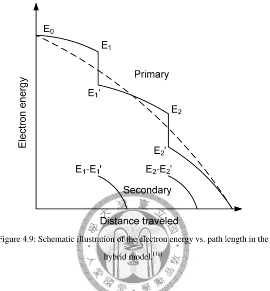
For the Monte Carlo simulation of secondary electrons, the Bethe-Blonch model mentioned in section4.2.5 should be replaced by a new model. Figure(4.9) shows the relation between electron energy and travel path. The dash line shows the energy spectrum with the regular continuous slowing down approximation proposed by Bethe.
The solid line represents the hybrid model. In the hybrid model, the primary electron energy decreases continuously unless ionization events occur. The trajectory of the
E le c tr o n e n e rg y
Figure 4.9: Schematic illustration of the electron energy vs. path length in the hybrid model.[11]
electron is divided into sections when a ionization event occurs at E1 and E2. The secondary electrons are then generated with energy of E1−E1′ and E2−E2′. The realization of this model is discussed in Murata’s work.[11]
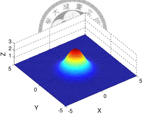
4.3 Gaussian Beam
Electron sources such as field emission can achieve sub-nanometer resolution on the sample. The shape and the current density are usually described by a 2D Gaussian function,
( 0)2 ( 0)2
2 2
( , ) exp
2σ 2σ
− −
= = − +
x y
x x y y
Z f x y A (4.19)
Here the coefficient A is the amplitude, x0, y0 is the center and σx, σy are the x and y spreads of the electron beam. In order to meet the actual condition in the Monte Carlo simulation, the landing position of the electron on the sample is calculated using the following equation,
4
0 5
4
0 5
2 log( )
cos(2 ) 3.3
2 log( )
sin(2 ) 3.3
π π
= − × ×
= − × ×
r R
X R
r R
Y R
(4.20)
where R4 and R5 are random variables uniformly distributed between 0 and 1. The electron beam radius r represents 99.9% of the total electron.
-5
0
5
-5 0
5 1 2 3
Y X
Z
Figure 4.10: 2D Gaussian distribution. The figure was created using A=3,
0 =0
x , y0 =0, σ =x 1, σ =y 1.
-20 -15 -10 -5 0 5 10 15 20 -20
-15 -10 -5 0 5 10 15 20
X
Y
Figure 4.11: 500 landing positions decided by equation (4.20) where the beam radius is 10nm.
4.4 Simulation Results
The simulation result was compared to the result of the publicly available Monte Carlo program CASINO.
4.4.1 Electron trajectories
The simulation results of the electron trajectories compared to CASINO are shown in the following figures in different incident energy.
-50 -40 -30 -20 -10 0 10 20 30 40 50 -120
-100 -80 -60 -40 -20 0
Figure 4.12: Monte Carlo simulation result of 200 trajectories of 300eV electron energy. The result of CASINO is on the left and the in-house MATLAB code is
on the right.
Figure 4.13: Monte Carlo simulation result of 200 trajectories of 500eV electron energy. The result of CASINO is on the left and the in-house MATLAB code is
on the right.
-50 -40 -30 -20 -10 0 10 20 30 40 50
-120 -100 -80 -60 -40 -20 0
Figure 4.14: Monte Carlo simulation result of 200 trajectories of 1000eV electron energy. The result of CASINO is on the left and the in-house MATLAB code is
on the right.
Figure 4.15: Monte Carlo simulation result of 200 trajectories of 2000eV electron energy. The result of CASINO is on the left and the in-house MATLAB code is
on the right.
-50 -40 -30 -20 -10 0 10 20 30 40 50
-120 -100 -80 -60 -40 -20 0
X
-50 -40 -30 -20 -10 0 10 20 30 40 50
-120 -100 -80 -60 -40 -20 0
X
4.4.2 Energy distribution
As the electrons strike the specimen, some of the energy carries by the electrons transfer to the specimen. The program segments the specimen into 3D meshes and accumulates the energy that was transferred to the specimen. The energy that accumulated into a single mesh is decided by the equation Ei =(dE dS/ )i×Li, where Li
is the electron path length that pass through the area, and (dE/dS)i is the energy loss equation.
(dE/dS)1
(dE/dS)2
Li
Figure 4.16: The electron trajectory in an XY plane.
The following figures show the energy distribution on the horizontal plane with different depth of the specimen.
The normalized mean squared error is one of many ways to quantify the amount of one matrix differs from another. It is defined to be
( )
( )
2
1
2
1
[ ] [ ] [ ]
N
r m
k N
m k
h k h k NMSE
h k
=
=
−
=
∑
∑ (4.21)
The simulation result of the energy distribution on an XY plane was compared to CASINO. The normalized mean squared error indicates the different between each other.
Table 4.4: The simulation result of the energy distribution.
CASINO in-house MATLAB NMSE
Z=-10 nm
-25 -20
-15 -10
-5 0
5 10
15 20
25 -25 -20 -15 -10 -5 0 5 10 15 20 25
0 0.2 0.4 0.6 0.8 1x 10⁻³
Y(nm) X(nm)
Amplitide (normalized)
-25 -20
-15 -10
-5 0
5 10
15 20
25 -25 -20 -15 -10 -5 0 5 10 15 20 25
0 0.2 0.4 0.6 0.8 1x 10⁻³
Y(nm) X(nm)
Amplitide (normalized)
0.4303
Z=-20 nm
-30 -20
-10 0
10 20
30 -25 -20 -15 -10 -5 0 5 10 15 20 25
0 1 2 3 4 5 6 x 10⁻⁴
Y(nm) X(nm)
Amplitide (normalized)
-20 -15
-10 -5
0 5
10 15
20 -20 -15 -10 -5 0 5 10 15 20
0 1 2 3 4 5 6 x 10⁻⁴
Y(nm) X(nm)
Amplitide (normalized)
0.2934
Chapter 5 Backscattered Electrons
The Monte Carlo simulation algorithm discussed in chapter five was coded by using MATLAB in this thesis. Since the backscattered electrons are considerable to design the detector array for multiple electron beam lithography system, each backscattered electrons’ information including the scatter direction, the balance energy, and the departure position is exported as a data file. The information of backscattered electron will be discussed in the following section.
5.1 Backscattering coefficient
In order to understand the behaviour of the backscattered electron in different energies, it is necessary to compare the theoretical predictions to some key measurements. One of the key measurements is the backscattering coefficient, η, which can be both relatively easily predicted theoretically and measured experimentally. It is usual to define η as the ratio of the backscattered electron current to the primary incident electron current,
η = b
p
I
I (5.1)
where Ib and Ip are the backscattered electron and primary electron current. In the simulation, the backscattered electron current will be replaced by the number of backscattered electron trajectories and the primary electron current will be replaced by the number of total electron trajectories in calculating the backscattering coefficient.
total of 24 samples were tested in the energy range 250-5000 eV. Several publicly available Monte Carlo programs were used to compare the backscattering coefficient to the experiment. The backscattering coefficient predicted by the Monte Carlo program coding by MATLAB in this thesis will be compared to Gomati’s work and other Monte Carlo program.
Figure 5.1: The experiment arrangement proposed by Gomati for backscattering coefficient.
Silicon Silicon
Backscattering coefficient
Figure 5.2: Experiments and Monte Carlo simulations of backscattering coefficient of silicon sample in different energies.
Figure(5.2) shows the experiments reported by Gomati in 2008 and Monte Carlo simulations of backscattering coefficient of silicon sample in different energies. The small ● stands for experiment data of as-inserted samples. The large ● stands for the cleaned samples, and the ▲ is data measured by Bronstein and Fraiman (1969).
The □ is the Monte Carlo simulation prediction according to Win X-ray. The △ is according to NISTMonte, and the ▽ is according to PENELOPE. The ╳ uses the continuous slowing down approximation of Joy and Luo (1989), and the ┼ uses the continuous slowing down approximation of Jablonski et al(2006). The blue lines with red □ is the Monte Carlo simulation prediction according to the in-house MATLAB
5.2 Energy distribution of backscattered electrons
Gain of an electron detector is related to the energy carried by the electrons. So it is important to analysis the energy distribution of backscattered electrons. Figure(5.3) shows the backscattered electron energy distribution of a simulation of a 1k eV electron beam striking on the silicon sample. The x-axis shows the energies of each group. The y-axis shows the percentage of the total amount of the backscattered electrons. The simulation results show that the energy of backscattered electrons centralizes to the incident energy of the primary electron beam. The number of backscattered electrons with low energy is compared to be very small.
100 200 300 400 500 600 700 800 900 1000
0 0.02 0.04 0.06 0.08 0.1 0.12 0.14 0.16 0.18 0.2
Backscattered electron energy
%
Silicon substrate Incident energy 1000eV 10k trajectories
Figure 5.3: Backscattered electron energy distribution
The sample is silicon. The incident energy is 1000 eV. 10k trajectories are simulated in this simulation. The backscattering coefficient η in this simulation is
0.20.
5.3 Multi-layer
Hydrogen silsesquioxane and PMMA are common resist for the electron beam lithography. In order to meet the real conditions of fabrication in Monte Carlo simulation, a layer of compound must be added on the substrate. Mean atomic number and mean ionization potential are used in Monte Carlo simulation for the compound.
The mean atomic number is defined by
=∑
av i i
i
Z c Z (5.2)
where ci is the mass concentration of the element Zi. Table(5.1) shows the mean atomic number and mean ionization potential for PMMA, ZEP520A, and HSQ.
Figure(5.4), Figure(5.5), and Figure(5.6) show the simulation result of backscattered electron energy distribution for different thickness of resist. The result shows that as the thickness of resist increase, the energy tends to centralize to higher level.
Table 5.1: Mean atomic number (Zav) and mean ionization potential for PMMA, ZEP520A, and HSQ.[10]
Zav J
PMMA [C5H8O2] 3.6 74.0 eV
ZEP520A [C13H15O2Cl] 4.1 84.8 eV
HSQ [(HSiO3/2)8] 7.7 109.0 eV
100 200 300 400 500 600 700 800 900 1000 0
0.02 0.04 0.06 0.08 0.1 0.12 0.14 0.16 0.18 0.2
Backscattered electron energy
%
10nm HSQ Silicon substrate Incident energy 1000eV 10k trajectories
Figure 5.4: Backscattered electron energy distributions for 10 nm HSQ on the silicon substrate. The backscattering coefficient η in this simulation is 0.17.
100 200 300 400 500 600 700 800 900 1000
0 0.02 0.04 0.06 0.08 0.1 0.12 0.14 0.16 0.18 0.2
Backscattered electron energy
%
20nm HSQ Silicon substrate Incident energy 1000eV 10k trajectories
Figure 5.5: Backscattered electron energy distributions for 20 nm HSQ on the silicon substrate. The backscattering coefficient η in this simulation is 0.20.
100 200 300 400 500 600 700 800 900 1000 0
0.02 0.04 0.06 0.08 0.1 0.12 0.14 0.16 0.18 0.2
Backscattered electron energy
%
30nm HSQ Silicon substrate Incident energy 1000eV 10k trajectories
Figure 5.6: Backscattered electron energy distributions for 30 nm HSQ on the silicon substrate. The backscattering coefficient η in this simulation is 0.24.
Chapter 6 Design and Optimization of the Detector Array
The backscattered electron information is used to decide some key parameters for designing of the detector arrays. The size of the detector is miniaturized in order to install on the multiple electron beam lithography system. The main difficulty of designing the architecture of the detector is that the signal grows dimmer as the size of the detector grows smaller. The main idea of the designing is to tend to collect the electron as much as possible.
Figure(6.1) shows the preliminary design of the detector architecture of beam position monitor system for multiple electron beam lithography system. The detectors are arranged to an array. These arrays will be placed above the wafer and the holes will let the primary electron beams to pass through. The width of one detector is
Figure 6.1: The preliminary design of the detector architecture of beam position monitor system for multiple electron beam lithography system.