Properties of nitrogen-implanted p-type ZnO films grown on Si 3 N 4 / Si by
radio-frequency magnetron sputtering
Chin-Ching Lin, San-Yuan Chen, Syh-Yuh Cheng, and Hsin-Yi Lee
Citation: Applied Physics Letters 84, 5040 (2004); doi: 10.1063/1.1763640 View online: http://dx.doi.org/10.1063/1.1763640
View Table of Contents: http://scitation.aip.org/content/aip/journal/apl/84/24?ver=pdfcov
Published by the AIP Publishing
Articles you may be interested in
p -type Zn 1 x Mg x O films with Sb doping by radio-frequency magnetron sputtering
Appl. Phys. Lett. 89, 202102 (2006); 10.1063/1.2388254
p-type semiconducting Cu 2 O–CoO thin films prepared by magnetron sputtering
J. Vac. Sci. Technol. A 21, 1336 (2003); 10.1116/1.1580491
Passivation of defects in nitrogen-doped polycrystalline Cu 2 O thin films by crown-ether cyanide treatment
Appl. Phys. Lett. 82, 1060 (2003); 10.1063/1.1555267
Growth and characterization of p-type HgTe/Hg 1x Cd x Te single quantum wells using nitrogen and arsenic
Appl. Phys. Lett. 79, 3980 (2001); 10.1063/1.1425465
Evaluation of densities and mobilities for heavy and light holes in p-type Hg 1x Cd x Te molecular beam epitaxy films from magnetic-field-dependent Hall data
J. Appl. Phys. 84, 4327 (1998); 10.1063/1.368652
This article is copyrighted as indicated in the article. Reuse of AIP content is subject to the terms at: http://scitation.aip.org/termsconditions. Downloaded to IP: 140.113.38.11 On: Thu, 01 May 2014 04:20:12
Properties of nitrogen-implanted
p
-type ZnO films grown on Si
3N
4Õ
Si
by radio-frequency magnetron sputtering
Chin-Ching Lin and San-Yuan Chena)
Department of Materials Science and Engineering, National Chiao-Tung University, 1001 Ta-hsueh Road, Hsinchu, Taiwan, R.O.C.
Syh-Yuh Cheng
Materials Research Laboratories, Industrial Technology Research Institution, Chutung. Taiwan, R.O.C.
Hsin-Yi Lee
Research Division, National Synchrotron Radiation Research Center, Hsinchu, Taiwan 300, R.O.C.
共Received 1 March 2004; accepted 23 April 2004; published online 28 May 2004兲
An nitrogen-implanted p-type ZnO film has been grown on a Si substrate buffered with Si3N4using
radio-frequency magnetron sputtering. The Si3N4 buffer layer can effectively improve film
stoichiometry and reduce the formation of oxygen vacancies compared to ZnO on Si. The electrical properties of the p-type ZnO films implanted with 5⫻1012– 1⫻1014 cm⫺2N⫹dose show a hole
concentration of 5.0⫻1016– 7.3⫻1017 cm⫺3, hole mobility of 2.51– 6.02 cm2/V s, and resistivity
of 10.11–15.3 ⍀ cm. The p-type ZnO films also showed an excellent crystallinity and a strong ultraviolet emission peak near 3.30 eV at room temperature. Moreover, as evidenced by extended x-ray absorption fine structure analysis, the local structure of the p-type ZnO films was changed due to the substitution of nitrogen ions for oxygen ions in p-type ZnO films. Our finding of p-type ZnO films grown on a Si3N4/Si substrate could provide a simple method to fabricate reproducible p-type
ZnO films on silicon substrate for the development of large-scale optoelectronic integration device. © 2004 American Institute of Physics. 关DOI: 10.1063/1.1763640兴
Wide-band-gap optoelectronics, especially for zinc oxide 共ZnO兲, are attracting more attention due to their potential applications in various fields, such as ultraviolet共UV兲 resis-tive coating, gas sensors, solar cells, and optical devices.1,2 For the development of ZnO-based optoelectronic devices, it is necessary to grow high-quality both p- and n-type ZnO thin films. The n-type ZnO is easily available even without any doping, while it has been recognized that it is very dif-ficult to obtain p-type ZnO because ZnO is a natural n-type semiconductor and the acceptors may have a natural ten-dency to pair with native defects or background impurities to form electrically inactive complexes although high densities of holes could be achieved with nitrogen as the dopant along with other techniques. Furthermore, the presence of native defects, such as zinc interstitials and oxygen vacancies, causes a deviation from stoichiometry.3In order to overcome this problem, recently, several research groups proposed many methods to obtain p-type ZnO films.4 –10 These thin-film growers have demonstrated that nitrogen will enter the ZnO films as shallower acceptor if N2, N2O, or NH3,
de-pending on the growing technique, is used as a source.11 It was well known that that as the ZnO films were de-posited on substrates, such as sapphire and silicon, a thin oxide layer 共probably amorphous SiO2) is easily grown on
its surfaces, and thus, more ‘‘extra defects’’ are easily in-duced to affect the defect equilibrium in ZnO films due to the formation of the thin oxide layer. On the other hand, in our previous study,12it was found that as Si3N4buffer layer was
deposited on Si prior to growing ZnO films, the defect con-centration of ZnO film on Si3N4/Si was much reduced that is
very close to characteristics of intrinsic semiconductor (e⫺: ⫺1.40⫻1014 cm⫺3).
In this letter, we have shown that high reproducible
p-type conduction ZnO films with high hole concentration
can be grown on Si buffered with Si3N4 by radio-frequency 共rf兲 magnetron sputtering along with nitrogen-implanted pro-cess. The role of nitrogen-implanted concentration in the electrical and photoluminescence,共PL兲 of ZnO films will be investigated. In addition, the exact origin of the UV emission and local structural behaviors of p-type ZnO films grown on Si3N4/Si is also discussed.
The ZnO thin films共⬃150 nm兲 were deposited on 4-in. Si substrates buffered with Si3N4 layers by rf magnetron
sputtering using 99.99% ZnO as a target. The buffer layers were grown by electron evaporation and the thickness of the Si3N4 buffer layers was measured to be about 40 nm by transmission electron microscopy. The as-grown ZnO film was subsequently subjected to nitrogen ion implantation at room temperature. The nitrogen ion with energy of 80 keV was injected into the as-grown ZnO films. The dose range studied was from 5⫻1012– 5⫻1015 cm⫺2. After ion im-plantation, the ZnO films were annealed at 850 °C for 20 min under pure nitrogen atmosphere.
The crystal structure was determined using Siemens D5000 x-ray diffraction共XRD兲 with Cu K␣ radiation and a Ni filter. PL measurement was performed by the excitation from 325 nm He–Cd laser at room temperature and 10 K. The electrical properties of the nitrogen-implanted ZnO films were investigated by van der Pauw method
room-a兲Author to whom correspondence should be addressed; electronic mail:
APPLIED PHYSICS LETTERS VOLUME 84, NUMBER 24 14 JUNE 2004
5040
0003-6951/2004/84(24)/5040/3/$22.00 © 2004 American Institute of Physics
This article is copyrighted as indicated in the article. Reuse of AIP content is subject to the terms at: http://scitation.aip.org/termsconditions. Downloaded to IP: 140.113.38.11 On: Thu, 01 May 2014 04:20:12
temperature Hall measurements with nonsintered indium contacts and magnetic field of 0.315 T. The x-ray absorption spectra were recorded at the wiggler beamline SL-17B at National Synchrotron Radiation Research Center 共NSRRC兲, Hsinchu, Taiwan.
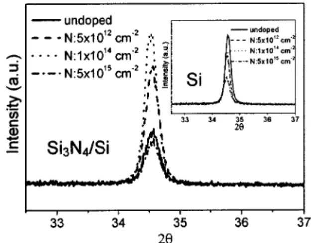
Figure 1 shows the XRD pattern of nitrogen ions (N⫹)-implanted ZnO thin films on Si and Si3N4/Si, and then annealed at 850 °C in N2 atmosphere. Only a sharp diffraction peak of共002兲 at 2⫽34.5° can be detected for all the ZnO films, indicating that these ZnO films were highly
c-axis oriented. However, as increasing the N⫹-implanted concentration form 5⫻1012 to 5⫻1015 cm⫺2, the intensity of the 共002兲 XRD peak in ZnO films grown on Si substrate decreases as shown in Fig. 1. This suggests that the im-planted N⫹ in ZnO film on Si presents a strong negative affect on crystalline characteristics of the ZnO films. In con-trast, when the ZnO films were grown on Si3N4/Si
sub-strates, it was found that 共002兲 diffraction peak becomes stronger with the increase of the implanted N⫹ from 5 ⫻1012to 1⫻1014 cm⫺2关Fig. 1兴. This reveals that the
occu-pation of the implanted N⫹ on oxygen vacancies can im-prove the crystallinity of ZnO films on Si3N4/Si. However,
above that, the peak intensity was rapidly decreased, imply-ing that more implanted N⫹ probably induces extra defects and this would lead to the lattice distortion.
The electrical conduction type of N⫹-implanted ZnO films as a function of doping doses is shown in Fig. 2. The N⫹-implanted ZnO films on Si substrate show n-type con-duction independent of the implanted N⫹ concentration. In sharp contrast, the N⫹-implanted ZnO films on Si3N4/Si substrate exhibit p-type conduction and the carrier concen-tration increases up to 7.3⫻1017 cm⫺3 with an increase of
N⫹-implanted concentration from 5⫻1012 to 1 ⫻1014 cm⫺2. According to our previous study, as the ZnO
films were deposited on the Si3N4/Si structure, x-ray
photo-electron spectroscopy analysis demonstrates that a lower oxygen vacancies concentration and thinner interface layer was detected for ZnO on Si3N4/Si structure compared to that
on Si.12 Furthermore, the film stoichiometry was improved because of the reduction in oxygen vacancies, indicating the ratio of Zn:O was decreased.13In this condition, the concen-tration of active acceptors may exceed the donor concentra-tion so that the conducconcentra-tion type was changed from n to p
type. The dependence of conduction type on the implanted N⫹ concentration in ZnO films in Fig. 2 suggests the N⫹-implanted process can product more holelike carries to transform original conduction 共compensate the native carri-ers兲. However, a further increase in the implanted dose of the N⫹up to 5⫻1015 cm⫺2leads to a decrease in hole concen-tration of p-ZnO and the conduction type of ZnO films would approach the intrinsic conductor.
Resistivity and Hall mobility as a function of implanted N⫹doses were measured and are shown in Fig. 3 for p-type conduction ZnO films. As increasing N⫹ doses from 5 ⫻1012 to 1⫻1014 cm⫺2, both hole concentration and Hall
mobility increase, but the resistivity decreases. The p-type ZnO films grown on Si3N4/Si show a hole concentration of
7.3⫻1017 cm⫺3, a mobility of 6.02 cm2/V s, and a low
re-sistivity of 10.3 ⍀ cm. Above that (1⫻1014 cm⫺2), both hole concentration and Hall mobility decreases, but an in-crease in resistivity was observed. The initial inin-crease in the hole concentration is due to a decrease in oxygen vacancy as the implanted N⫹ doses increase. The decrease in hole con-centration after the maximum value is caused by the forma-tion of more defects due to excess N⫹ that can compensate for a hole carrier which may correspond to the degradation of the crystal quality in p-type ZnO films as supported by the decrease in the peak intensity of 共002兲 XRD peak in Fig. 1 FIG. 1. XRD patterns of ZnO films sputtered at Si, and Si3N4/Si substrates
with or without N⫹-implanted various doses.
FIG. 2. Electrical conduction type of N⫹-implanted ZnO films as a function of various doses.
FIG. 3. Variation of resistivity and Hall mobility as a function of different N⫹implanted doses.
5041
Appl. Phys. Lett., Vol. 84, No. 24, 14 June 2004 Linet al.
This article is copyrighted as indicated in the article. Reuse of AIP content is subject to the terms at: http://scitation.aip.org/termsconditions. Downloaded to IP: 140.113.38.11 On: Thu, 01 May 2014 04:20:12
for the N⫹-implanted ZnO film with the dose of 5 ⫻1015 cm⫺2.
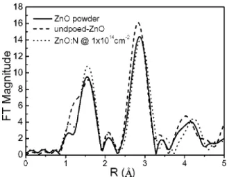
In order to further understand the local structure of
p-type ZnO films, the extended x-ray absorption fine
struc-ture was investigated. Figure 4 shows the pseudoradial dis-tribution functions obtained from the k3-weighted Fourier transforms at Zn K edge for the nonimplanted and N⫹-implanted ZnO films on a Si3N4/Si structure annealed at
850 °C in N2atmospheres, where pure ZnO powder was used
as standards for comparison. The first peak in the Fourier transforms corresponds to the nearest-neighbor distance around zinc atoms. The peak position of zinc to oxygen for both bulk powder standards 共ZnO: 99.999%兲 and nonim-planted ZnO thin films is equal to 1.945 Å. For the ZnO film implanted with 1⫻1014 cm⫺2N⫹ dose, the Zn—O bond length in ZnO/Si3N4/Si is very similar to that of
nonim-planted ZnO films and bulk powder standards. However, for the second nearest-neighbor distance around Zn2⫹, it was found that the Zn—Zn bond length for nonimplanted ZnO films is shorter than that of N⫹-implanted ZnO films. It could be due to the existence of oxygen vacancies in the ZnO lattice matrix that causes the secondary nearest-neighbor dis-tance to become shorter. In comparison with bulk powder standards共3.27 Å兲, a little larger Zn—Zn bond length 共3.28 Å兲 was also detected for N⫹-implanted ZnO films. These observations suggest that the implantation of N⫹ into ZnO films could affect the local structure of ZnO film, such as bond distance, but a limited range of 1⫻1014 cm⫺2 N⫹
dose can effectively improve the crystal quality of ZnO films.
Figure 5 illustrates the room-temperature PL spectrum of ZnO films implanted with various N⫹ doses on Si3N4/Si
substrates. UV emission with peaks at 3.31, 3.28, 3.29, and 3.30 eV is dominantly observed for the ZnO films implanted with 0, 5⫻1012, 1⫻1014, and 5⫻1015 cm⫺2N⫹ dose, re-spectively. According to the spectrum, it is noticed that the peak intensity of the UV emission depends markedly on the N⫹-implanted dose. The ZnO film implanted with a 1 ⫻1014 cm⫺2N⫹dose not only shows a stronger peak
inten-sity but also has a narrower full width at half maximum of 95
meV than that 共110 meV兲 of nonimplanted ZnO films. In addition, the deep level emission in the ZnO-implanted with 5⫻1012– 1⫻1014 cm⫺2N⫹dose samples were almost cov-ered by the background signal. In contrast, a weak deep-level emission at around 2.055 eV and 2.015 eV can be observed in nonimplanted and implanted with 5⫻1015 cm⫺2N⫹dose sample, respectively. It means the point defects dominating the visible transition can be improved by suitable N⫹doping. In summary, we report on the reproducible p-type ZnO films grown on Si3N4/Si by rf magnetron sputtering, im-planted with 5⫻1012– 1⫻1014 cm⫺2N⫹ dose and then an-nealed at 850 °C in N2ambient. The hole concentration, car-rier mobility, and resistivity of p-type ZnO films were 5.0 ⫻1016– 7.3⫻1017 cm⫺3, 2.51– 6.02 cm⫺2V s, and 10.11–
15.3 ⍀ cm, respectively. PL spectra of the N⫹-implanted ZnO/Si3N4/Si showed a sharp UV emission and invisible
deep-level transition at room-temperature measurement. These results suggest that N⫹-implanted ZnO films depos-ited on a Si buffer with Si3N4 show electrical and optical
behaviors that make them excellent candidates for a good
p-type layer for ZnO-based optoelectronic device on a
Si-based substrate.
The authors gratefully acknowledge the National Sci-ence Council of the Republic of China for its financial sup-port through Contract No. NSC-92-2216-E-009-014.
1
T. Soki, Y. Hatanaka, and D. C. Look, Appl. Phys. Lett. 76, 3257共2000兲.
2
K. Hummer, Phys. Status Solidi 56, 249共1973兲.
3T. Yamamoto and H. Yoshida, Physica B 302, 155共2001兲.
4K. Iwata, P. Fons, A. Yamada, K. Matsubara, and S. Niki, J. Cryst. Growth
209, 526共2000兲.
5
T. Yamamoto and H. Yoshida, Jpn. J. Appl. Phys., Part 2 38, L166共1999兲.
6K. Nakahara, H. Takasu, P. Fons, A. Yamada, K. Iwata, K. Matsubara, R.
Hunger, and S. Niki, Appl. Phys. Lett. 79, 4139共2001兲.
7M. Kasuga and S. Ogawa, Jpn. J. Appl. Phys., Part 1 22, 794共1983兲. 8Y. Sato and S. Sato, Thin Solid Films 281, 445共1996兲.
9
J. J. Lander, J. Phys. Chem. Solids 9, 324共1960兲.
10X.-L. Guo, H. Tabata, and T. Kawai, J. Cryst. Growth 223, 135共2001兲. 11M. Joseph, H. Tabata, H. Saeki, K. Ueda, and T. Kawai, Physica B 302,
140共2001兲.
12
C. C. Lin, S. Y. Chen, and S. Y. Cheng, Electrochem. Solid-State Lett. 7, J20共2004兲.
13S. H. Bae, S. Y. Lee, B. J. Jin, and S. Im, Appl. Surf. Sci. 154, 458共2000兲.
FIG. 4. Fourier transforms at Zn K edge for the ZnO powder standards,
nonimplanted, and N⫹-implanted ZnO/Si3N4/Si samples. FIG. 5. Room-temperature PL spectra of nonimplanted and N
⫹-implanted
ZnO/Si3N4/Si samples.
5042 Appl. Phys. Lett., Vol. 84, No. 24, 14 June 2004 Linet al.
This article is copyrighted as indicated in the article. Reuse of AIP content is subject to the terms at: http://scitation.aip.org/termsconditions. Downloaded to IP: 140.113.38.11 On: Thu, 01 May 2014 04:20:12