國立交通大學
材料科學與工程研究所
碩士論文
利用邊緣移動方法研究純錫薄膜之電遷移
STUDY OF ELECTROMIGRATION IN THIN TIN
FILM USING EDGE DISPLACEMENT METHOD
指導教授:陳智 博士
研究生:尤宏誌
STUDY OF ELECTROMIGRATION IN THIN TIN
FILM USING EDGE DISPLACEMENT
METHOD
Master Thesis
Department of Materials Science and Engineering
Nation Chiao-Tung University
Hsinchu, Taiwan
Republic of China
Prepared by: Hung-Chih Yu
Directed by: Chih Chen
致謝
感謝恩師 陳智教授在學業上的與生活上的指導與關懷,使學生 可以對這領域的研究有更寬廣的看法與更深一層的認知。 承蒙口試委員:高振宏老師、謝宗庸老師、陳信文老師的細心審 閱以及提供許多寶貴的意見,讓這篇論文更加完整。 此外還要感謝實驗室的幾位學長: 許穎超學長、劉書宏學長、楊 慶榮學長、林鈺庭學長、邱聖翔學長、魏程昶學長以及同學黃章斌、 陳筱芸的大力協助,才能將此論文順利完成。最後,將這兩年來心血 完成的論文獻給一直默默支持我的家人。謝謝每一位曾經幫助我的 人,願與你們分享這份喜悅。 尤宏誌 July 21, 2005利用邊緣移動方法研究純錫薄膜之電遷移
學生: 尤宏誌 指導教授: 陳智博士 國立交通大學材料研究所 摘要 本實驗利用邊緣移動方法測量純錫薄膜的電遷移行為,並求得 其電流的門檻電流密度以及其他參數。我們在矽晶片上面先鍍上一層 1200 Å 的鈦膜,隨後在鈦膜上面鍍 5000 Å厚的錫膜,在室溫(27 ℃~32 ℃)、50 ℃、75 ℃和 100 ℃下,對純錫薄膜加以 2.5 × 10⁴ A/cm2 到 1.5 × 10⁵ A/cm2的電流密度,並觀察電遷移效應。實驗結果發現在 室溫以及 50 ℃下在陽極皆有看到針狀與島狀的錫凸塊,但是在 75 ℃ 和 100 ℃下在陽極只有見到島狀錫凸塊的生成,且在四個通電的環境 溫度下,錫原子的漂移速率皆隨著電流密度增加而上升。實驗求得門 檻電流密度在室溫、50 ℃、75 ℃和 100 ℃下分別為 1.93 × 10⁴、9.65 × 10³、9.57 × 10³ 和 7.93 × 10³ A/cm2,並且求得純錫的電遷移活化能 為 0.32 eV。此外,在室外下由不同的錫條長度所算出的臨界長度為 18 µm且由實驗結果計算得知純錫薄膜的DZ*值在室溫、50 ℃、75 ℃ 和 100 ℃下分別為 1.95 × 10⁻¹⁰、4.84 × 10⁻¹⁰、1.27 × 10⁻⁹和 1.99 × 10⁻⁹ cm2/s。由於在無鉛銲料中錫的成分佔的比率皆相當高,所以這些純 錫電遷移的基本研究顯得非常的重要。STUDY OF ELECTROMIGRATION IN THIN TIN FILM USING EDGE DISPLACEMENT METHOD
Student: Hung Chih Yu Advisor: Chih Chen Department of Materials Science and Engineering
Nation Chiao-Tung University
Abstract
Threshold current density and other electromigration parameters of pure Tin (Sn) films were measured using edge displacement method. Sn film with a thickness of 5000 Å was evaporated on a 1200Å-thick Ti film on a Si substrate. Electromigration behavior was investigated under the current densities of 2.5 × 10⁴ to 1.5 × 10⁵ A/cm2 at room temperature (R.T. = 27 ℃~32 ℃), 50 ℃, 75 ℃ and 100 ℃. Both needle-type and hillock-type whiskers grew in the anode end when the films were stressed at R.T. and 50 ℃, but only hillock-type whiskers were observed when they were stressed at 75 ℃ and 100 ℃. The electromigration rate increased linearly with the applied current density for the four stressing temperatures. The threshold current density (Jc) was measured to be 1.93 × 10⁴, 9.65 × 10³, 9.57 × 10³ and 7.93 × 10³ A/cm2 for R.T., 50 ℃, 75 ℃ and 100 ℃, respectively. The measured activation energy was 0.32 eV. In addition, the measured critical length of the Sn film was 18 µm at R.T. and the products of DZ* were 1.95 × 10⁻¹⁰, 4.84 × 10⁻¹⁰, 1.27 × 10⁻⁹
and 1.99 × 10⁻⁹
Contents
Abstract in Chinese ...I
Abstract ... II
Contents... III
List of figures ... V
List of tables ... VIII
Chapter1 Introduction... 1
Chapter2 Literature Review ... 4
2.1 Electromigration theory... 4
2.2 Edge displacement method... 6
2.3 Backflux and critical length... 9
2.4 Mean-time-to-failure (MTTF) ... 10
2.5 The electromigration behavior in solders ... 12
2.6 The effect of electromigration on the interface... 17
2.7 The melting phenomenon in solder bumps... 21
Chapter3 Experimental... 24
3.1 Fabrication of samples... 24
Chapter4 Results and Discussion ... 30
4.1 Microstructure evolution ... 30
4.2 Threshold current density (Jc) ... 41
4.3 Activation energy ( Ea ) and DZ*... 41
4.4 Critical length ... 46
Chapter5 Conclusions... 50
List of figures
The cross-sectional view of the Blech structure after stressing ... 7 FIG. 2.1
The plot of drift velocity against current density ... 7 FIG. 2.2
(a) schematic illustration of Sandwich structure (b) SEM image of Sn-Pb solder stressed at 1×10⁵ A/cm2 at room temperature for 19 days ... 12 FIG. 2.3
The hillocks formed in the alloy, which has different Sn, Pb composition, stressed at 105 A/cm2 for 40 h... 13 FIG. 2.4
Cross-sectional-view of SEM images of eutectic SnPb solder bumps stressed under the current of 1.5 Amp and 120℃. ... 15 FIG. 2.5
SEM images of the cross-sectional view of Sn3.8Ag0.7Cu solder bumps stressed under the current of 1.5 Amp and 120℃. ... 16 FIG. 2.6
(a) the structure of V-groove; (b) the cross-sectional view of the V-groove. ... 17 FIG. 2.7
(a) Surface morphology of V-groove after stressing (a) 2.8 × 10⁴ A/cm2 at 150℃ for 8 days; (b) the void at the cathode side of V-groove; (c) 5.7 × 10⁴ A/cm2 at room temperature for 12 days. ... 19 FIG. 2.8
The intermetallic compound formed at the cathode side and the anode side after stressing at 5.7 × 10⁴ A/cm2 at 180℃ (a) o h at anode side; (b) 10 h at anode side; (c) o h at the cathode side; (d) o h at cathode... 20 FIG. 2.9
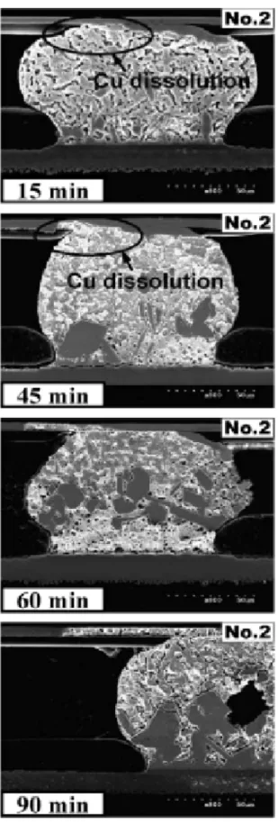
The Cu UBM melted asymmetrically due to current crowding.... 22 FIG. 2.10
The plot of length of the dissolved Cu trace against time of stressing time. ... 23 FIG. 2.11
The three left pictures and three right pictures are the procedure to prepare the testing samples ... 25 FIG. 3.1
Schematic illustration of the cross-sectional view of the Sn Blech specimen... 26 FIG. 3.2
AFM (atomic force microscope) was used to measure the cross-sectional area of the cathode side of the Sn stripes ... 28 FIG. 3.3
Plan-view SEM image of the fabricated sample ... 29 FIG. 3.4
Plan-view SEM images of the cathode side stressed at R.T... 31 FIG. 4.1
FIG. 4.2 Plan-view SEM images of the cathode side stressed at 50℃ ... 33 FIG. 4.3 Plan-view SEM images of the cathode side stressed at 75℃ ... 34 FIG. 4.4 Plan-view SEM images of the cathode side stressed at 100℃ ... 35
Plan-view SEM images of the cathode side after the current stressing by 1.25 × 10⁵ A/cm2... 37 FIG. 4.5
Drift velocity of the Sn stripe as a function of current density at R.T., 50 ℃, 75 ℃ and 100 ℃... 38 FIG. 4.6
Plan-view SEM images of the anode side after the current stressing by 5 × 10⁴ A/cm2... 39 FIG. 4.7
The increase in temperature due to the applied current density detected by the Infrared technique ... 42 FIG. 4.8
The plot of ln ( VT / j ) against 1/T. Activation energy can be obtained by the slope of the fitting curve ... 44 FIG. 4.9
Plan-view SEM images of the cathode side stressed under the current density of 1 × 10⁵
A/cm2 at room temperature for 53.5 h on different stripe lengths ... 48 FIG. 4.10
The plot of drift velocity against the reciprocal of the stripe length. The critical length was estimated to be 18 µm... 49 FIG. 4.11
List of tables
TABLE I. Testing currents, temperatures, corresponding drift velocities, and
Chapter 1 Introduction
In the semiconductor industry, flip-chip technology has been widely used for high-density packaging because of its capacity to handle large numbers of input-output (I/O).1,2 Due to the trend of miniaturization and the high performance, the dimension of solder bumps keeps decreasing and the current that each bump needs to carry keeps increasing, causing the current density in the solder bump to increase dramatically. Under the stressing of that high current density, the electrons flowing from the cathode side to the anode side may hit the atoms simultaneously so that atoms would move in the same direction as the electrons do. Gradually, as the atoms keep leaving from the cathode side, voids would be formed and finally make the circuit broken. At the anode side, the extrusion of the atoms, such as hillocks or whiskers, may contact with another circuit. This phenomenon would cause short-cut in the integrated circuit. Therefore, electromigration (EM) has become an important reliability issue in flip-chip solder joints.3-6
On the other hand, the eutectic SnPb solders have gradually been replaced by Pb-free solders due to environmental concern of Pb pollution.7-8 Among the most promising candidates for Pb-free solders, such as SnAg3.5 and SnAgCu, Sn constitutes over 95 %, and the matrix of the solder is almost pure Sn after reflow.9 Since the Ag and Cu atoms react with Sn or other materials in under bump metallization (UBM) to form Ag3Sn, Cu-Sn, or Cu-Ni-Sn intermetallic compounds (IMCs),5,10,11 the EM study in pure Sn is fundamental for understanding the
electromigration in Pb-free solders.
In 1976, Blech designed a test structure for EM study, from which electromigration rate and other parameters could be measured.12 It is often called “Blech specimen” or “edge displacement method”. The activation energy can be obtained by the Nernst-Einstein equation13
V = J/N = BeZ*
ρ
j = (D0 /kT)e Z *ρ
j exp( -Ea/kT ), (1.1) where V is the drift velocity, J is the atom flux, N is the density of metal ions, B is mobility, eZ* is the effective charge number of ions,
ρ
is the metal resistivity, j is the electric current density, D0 is the diffusionpreexponential factor, k is the Boltzmann’s constant, T is the absolute temperature, and Ea is the activation energy. Z* can be also obtained if the diffusivity of the material is known. Equation (1) can be written as the following equation: ⎟⎟ ⎠ ⎞ ⎜⎜ ⎝ ⎛ + − = ⎟⎟ ⎠ ⎞ ⎜⎜ ⎝ ⎛ ∗ k eZ D kT Ea j VT o ρ ln ln (1.2) Thus, Ea can be obtained from the slope of the linear relation on the plot of ⎟⎟ ⎠ ⎞ ⎜⎜ ⎝ ⎛ j VT ln versus T 1
. In addition, the threshold current density (Jc) can be obtained by extrapolating the plot of drift velocity against the applied current density to zero drift velocity, which represents the maximum allowable current that Sn can carry without EM damage. Critical length can also be estimated by measuring the EM rate at different lengths of Sn stripes.14
Sun and Ohring obtained an activation energy of 0.45 eV/atom and an effective charge number of -49 to -85 for pure thin Sn film by tracer self-diffusion.15 Liu et al. also reported the EM rate in Sn film by using
the edge displacement method.16 However, threshold current density and critical length for pure Sn have not been reported. Threshold current density represents the maximum current density below which no electromigration occurs, and critical length denotes the length of the stripe below which no EM damage takes place. They are very important parameters for characterizing the electromigration behavior in pure Sn.
In this study, we employed the edge displacement method to measure the electromigration parameters for Sn film, including drift velocity at various temperatures and current densities, threshold current density, activation energy, effective charge number, and critical length. These parameters will be fundamental for the electromigration in Pb-free solders.
Chapter 2 Literature review
2.1 Electromigration theory
Electromigration (EM) is a phenomenon of a combination of thermal an electrical effects on mass motion. For a bulk metal, electromigration occurs at about three-quarter of its melting point (in absolute temperature). For a metallic polycrystalline thin film, electromigration occurs at about half of its melting point (in absolute temperature). A large number of atoms at this temperature would undergo random walk processes in the lattice and grain boundaries for the bulk and the thin film, respectively.
When a thin film stripe is stressed under a high current density, the electrons would hit the atoms at the cathode side and the momentum would be exchanged between electrons and diffusing atoms. This phenomenon is formed by the interaction of two different types of force:
1. Coulombic force: the force between the electrostatic force and metal ion, when an external electric field is applied.
2. Electron wind force: the force made by the momentum exchange between electrons and diffusing atoms.
The atomic diffusion flux in a solid can be written as:17
∑
+
∂
∂
−
=
i i iF
CM
X
C
D
J
(2.1) Where the first term represents the mass transport resulted from chemical potential gradient, and the second term represents mass transport contributed by the sum of different forces. For a pure metal, there is no chemical potential gradient between the atoms, so the first term is zero. The second term is what we discussed above, the combination of directaction of the electrostatic field and the momentum exchange of electrons and diffusing atoms. For simplicity, the second term can be written as:17
el wd (2.2) i i i
F
F
F
CM
=
+
∑
By comparing the magnitudes between the electrostatic field force and the electron wind force, we know that the electron wind force is much bigger than the electrostatic field force so that the atoms would be pushed from the cathode side to the anode side. Besides, the dominative term Fwd can be written as:13
e
EZ
F
wd=
*
(2.3)where E is the electric field, Z* is the effective charge number. Z* is a parameter to express how the atoms would migrate when they are effected by electromigration. So, the Z* value varies from different metals. We can combine equations (2.1) and (2.2):17
wd
CMF
J
=
(2.4)where M is the mobility of the atoms and C is the atomic concentration. By using the Einstein equation, the mobility can be written as:
KT
D
M
=
(2.5)where D is the diffusivity, K is the Boltzmann’s constant, T is the absolute temperature. Now, we can combine equations (2.3), (2.4) and (2.5), to obtain the following equation:
eE
Z
KT
D
C
CMF
J
em=
wd=
*
(2.6)2.2 Edge displacement method
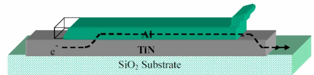
In 1976, Blech designed a test structure for electromigration study, from which electromigration rate and other parameters could be measured.12,18,19 The structure used in the study is shown in figure 2.1. Aluminum thin film was deposited on TiN, which is a high resistivity metal material, and then a high current density was applied from one side to another. In this structure, because TiN is a high resistivity layer compared to aluminum layer, most of the current would go through the aluminum layer instead of TiN layer in the experiment. So, it is pragmatic design to understand the mass transportation due to the electromigration phenomenon by observing voids at the cathode side and hillocks at the anode side. Drift velocities were also obtained in the study by the relation between the depleted mass and the stressing time. Figure 2.2 is the plot of current density against drift velocity for a stripe of 115, 25 and 115µm for its length, width and thickness, respectively.
From figure 2.2, we can find that there is a linear relationship between drift velocity and the applied current density, and the linear line has an intersection point with current density-axis. The physical meaning of the phenomenon is that the applied current density must be larger than a certain number, below which no electromigration phenomena would have influence on the diffusion of the atoms. This intersection point is called
the
FIG. 2.1. The cross-sectional view of the Blech structure after stressing.
FIG. 2.2. The plot of drift velocity against current density. The samples were annealed at 500℃ for 0.5 h.
the threshold current density. Each stripe length corresponds to a certain threshold current density. The reason for this phenomenon is because there is a backflux which resists the occurrence of electromigration.12,19 When there is a current passing through a stripe, the atoms would deplete from the cathode side and aggregate at the anode side. During this process, a stress would accumulate in the aluminum stripe, if there is a native oxide on the thin film. So, when atomic migration occurs, there is a compressive stress at the anode side due to the aggregate of the atoms from the cathode side; on the other hand, a tensile stress occurs at the cathode side, since atoms are moved away by electrons. The stress gradient between the two sides of the thin film stripe would lead to the occurrence of the backflux. We can express the backflux by the following relationship:20
)
(
a vx
KT
D
C
J
σµ
−
µ
∂
∂
=
(2.7)where
µ
a is the chemical potential of atoms,µ
v is the chemical potential of vacancies. A thermal equilibrium, the chemical potential can be written as follows:20 n v aµ
µ
σ
µ
µ
=
(
−
)
=
0−
Ω
(2.8)where
µ
0 is chemical potential in the stress free crystal, is atomicvolume,
Ω
n
σ
is the normal stress on the grain boundary. The backfluxx
KT
D
C
J
n∂
∂
Ω
=
σ
σ (2.9)2.3 Backflux and critical length
From the discussion above, we can conclude that there is a specific threshold current density for each strip length. Besides, it is known that when atoms are gradually moved from the cathode side to the anode side, a stress gradient established between the two sides of the stripe and this phenomenon is the reason for the formation of backflux. When the applied current density is below the threshold current density, the drift velocity is zero, and the relation can be written as:
σ
J
J
em=
(2.10)Combing equations (2.6), (2.9) and (2.10), we obtain the following equation:
x
j
eZ
n∂
∂
Ω
=
σ
ρ
*
(2.11)ρ
σ
*
)
(
eZ
l
j
th critΩ∆
=
⋅
(2.12) The equation above is derived by Blech and the critical product (j·l)crit is in the range of 500~2000 Å/cm for the pure aluminum stripe at 225℃.202.4 Mean-time-to-failure (MTTF)
Electromigration is a atomic migration behavior driven by the electrons. When the phenomenon is occurred, the resistance of the circuit would increase and cause the joule heating to increase the temperature of the integral circuit. So, mean-time-to-failure (MTTF) is a reference for the semiconductor industry to test the reliability of the device.
Generally speaking, when the resistance increases to about 20%, the device is termed as failed. Mean-time-to-failure is able to predict the life time of electric device stressed under a certain current density and certain temperature. The equation that used for predicting the life time is called Black’s equation.
)
exp(
KT
Q
j
A
MTTF
=
n (2.13) where A is a constant, j is the applied current density, n is an order parameter, Q is the activation energy for failed device. However, when electric current is applied into solder bumps, there must be a current crowding region at the entrance of solder bumps, so the current density would increase dramatically between the solder bumps and the circuit. At this time, the high current density leads to joule heating so that the temperature would increase dramatically. Equation 2.13 must be modified so that there is no great difference with the correct time predicted by MTTF. The equation should be modified as follows:)
)
(
exp(
)
(
K
T
T
Q
Cj
A
MTTF
n∆
+
=
where C is the modification of the current density, the
∆
T
is the modification of the temperature increase due to joule heating.212.5 The electromigration behavior in solders
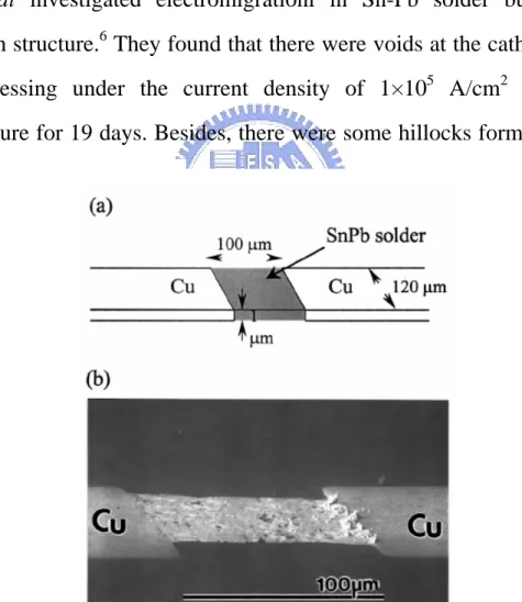
In recent years, due to the trend of miniaturization and the high performance of electronic products, the dimensions of integrated circuit shrink and the current that the circuit needs to carry keeps increasing, which increases the current density in the circuit dramatically, and so do the solder bumps. Therefore, there are numerous electromigration studies related to solder bumps. The damage mechanism of the solder bumps by electromigration is very similar with that of aluminum circuit. In 1999, Liu et al investigated electromigrationi in Sn-Pb solder bumps by sandwich structure.6 They found that there were voids at the cathode side after stressing under the current density of 1×10⁵ A/cm2 at room temperature for 19 days. Besides, there were some hillocks formed at the anode side, as shown in figure
FIG. 2.3. (a) schematic illustration of Sandwich structure (b) SEM image of Sn-Pb solder stressed at 1×10⁵ A/cm2 at room temperature for 19 days.
anode side, as shown in figure 2.3.
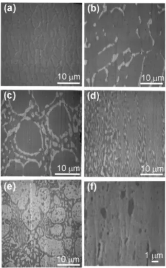
Because most of the solders constitute at least 2 different metals, the diffusion mechanism of solder bumps is something different from that of the circuit, made of pure copper or pure aluminum. Figure 2.4 shows the SEM images of hillocks formed in the pure Sn, Sn80Pb20, Sn70Pb30, eutectic Sn63Pb37, Sn40Pb60, Sn5Pb95, which are stressed under the current density of 105 A/cm2 for 40 h.22
FIG. 2.4. The hillocks formed in the alloy, which has different Sn, Pb composition, stressed at 105 A/cm2 for 40 h (a) pure Sn; (b) Sn80Pb20; (c) Sn70Pb30; (d) eutectic Sn63Pb37; (e) Sn40Pb60; (a) Sn5Pb95.
In SEM images, we can find that hillocks grew more easily at grains. Besides, we also find that the diffusion behavior is more active when the alloy is of eutectic composition, because they provide more diffusion interface in this region, so hillocks are more easily found in the eutectic phase region in Sn-rich alloy, as shown in figure 2.4 (b) and (c). If we compare figures 2.4 (a) to (f), it is easy to find that the Pb-rich alloy possesses more resistance to EM in comparison with Sn-rich does. That is to say, for the Sn-Pb alloy, although Sn is the dominative factor for diffusion, the resistance to electromigration still depends on the microstructure of the solder.
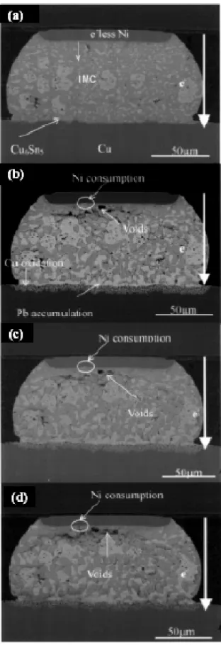
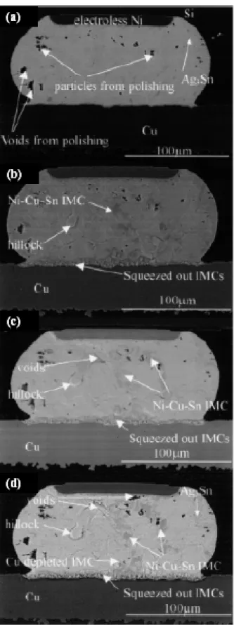
Besides, Lee et al. investigated the migration of the Pb-phase in eutectic SnPb and Sn3.8Ag0.7Cu solders for flip chip solder bumps. Figure 2.5 is the cross-sectional view of the eutectic SnPb solder stressed under the current of 1.5 Amp amd 120℃. One can see that Pb-rich component moves to the anode side and leaves voids at the cathode side due to electromigration and the Ni layer in UBM would melt due to the increase of temperature by joule heating. The reason is that when temperature is above 100℃, Pb is the dominative migration species. For lead-free solders, such as Sn3.8Ag0.7Cu, Lee et al. found that the extrusion was formed at the anode side, as shown in figure 2.6. Below the extrusion, Lee also found that Cu UBM would generate oxidation particles after current stressing.23
FIG. 2.5. Cross-sectional-view of SEM images of eutectic SnPb solder bumps stressed under the current of 1.5 Amp and 120℃. (a) o h; (b)20 h; (c)30 h; (d)39.5 h.
FIG. 2.6. SEM images of the cross-sectional view of Sn3.8Ag0.7Cu solder bumps stressed under the current of 1.5 Amp and 120℃. (a) o h; (b)20 h; (c)110 h; (d)200 h.
2.6 The effects of electromigration on the interface
When soldering, the low-melting-point solder bumps would melt and react with the high-melting-point metal on the board side to form the joint, so the IMCs formed at the metal/solder interface becomes an important issue. Many papers reported that the IMCs at the interface affect directly or indirectly on the properties of the device, such as chemical properties, electric properties, etc.24-26
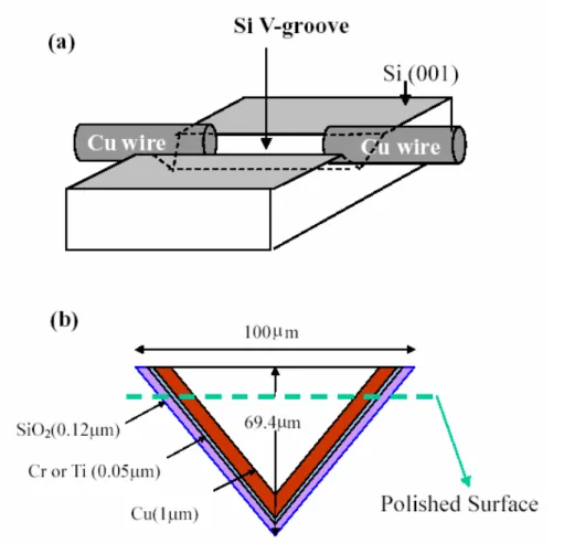
Huynh et al. designed a V-groove with two segment of Cu wire at the two sides, as shown in figure 2.7.27 He found that the eutectic SnPb sold
FIG. 2.7. (a) the structure of V-groove; (b) the cross-sectional view of the V-groove.
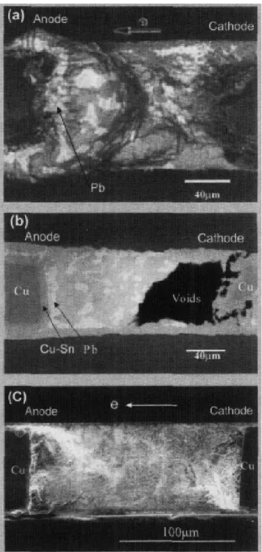
solder in theV-groove has different surface morphology evolution after stressing at different temperatures due to electromigration. As shown in figure 2.8, which is the SEM image of the solder bumps stressed for 8 days, there are hillocks formed at the anode side, but there are no depletion phenomena at the cathode side. However, after polishing to remove 10-µm-thick solder bump, it is easy to observe the voids formed at the cathode side, as shown in figure 2.8 (b). However, when the solder is tested under the room temperature, no voids and hillocks can be seen at the cathode side and the anode side, respectively, as shown in figure 2.8 (c).27
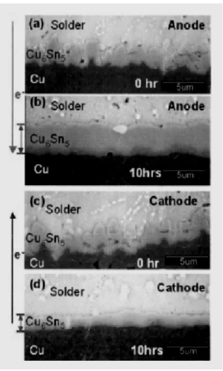
As to IMCs, they found that electromigration promotes the growth of IMCs. As shown in figures 2.9 (a) to (b), figure 2.9 (b) exhibits thicker Cu6Sn5 at the cathode side compared with the solder which is not stressed by current. For the interface at the anode side, the growth of the intermetallic compound is not as fast as the cathode side after stressing for 10 h.28, 29 From what has been discussed above, we may conclude that electromigration not only changes the distribution of the composition in the solder, but also changes the growth of the interetallic compound at the interface.
FIG. 2.8. (a) Surface morphology of V-groove after stressing (a) 2.8 × 10⁴ A/cm2 at 150℃ for 8 days; (b) the void at the cathode side of V-groove; (c) 5.7 × 10⁴ A/cm2 at room temperature for 12 days.
FIG. 2.9. The intermetallic compound formed at the cathode side and the anode side after stressing at 5.7 × 10⁴ A/cm2 at 180℃ (a) o h at anode side; (b) 10 h at anode side; (c) o h at the cathode side; (d) o h at cathode.
2.7 The melting phenomenon in solder bumps
In general, the failure usually starts at the interface of the solder bumps and the circuit. Due to this phenomenon, Yeh attributed the failure mechanism to the current crowding. So, the current crowding phenomenon is another key issue to determine how the device is affected by the electromigration. Current crowding phenomenon usually happens at the corner when electrons flow from the circuit to the solder bumps. That means the current density at this point increases dramatically, due to current crowding phenomenon.
Figure 2.10 shows the Cu UBM on the top of the solder bump has asymmetric melting phenomenon after current stressing.30 Hu pointed out that the Cu UBM would melt into solder bumps when stressing under the current of 1.27 A at 100℃, due to the local joule heating at the contact window. The Cu UBM on the chip side would be pushed into solder bumps to form IMCs after stressing for 15 mins, as shown in figure 2.10. Few minutes later, the Cu layer of the UBM would be consumed gradually and the solder replaced the location which is occupied by Cu originally. Finally, the solder filled in the Cu circuit and the device failure occurred.
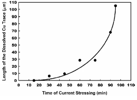
Hu also found that the Cu atoms are pushed from the cathode side to the anode side by electrons and reacted with Sn to form a large amount of Cu6Sn5 IMCs at the anode side, which is in deeper color in the solder bumps shown in the figure 2.10. On the other hand, the average dissolved rate of Cu atoms is calculated to be 1 µm/min by the relation between the length of the dissolved Cu trace and the stressing time, as shown in figure 2.11.
FIG. 2.11. The plot of length of the dissolved Cu trace against time of stressing time.
Chapter 3 Experimental
3.1 Fabrication of samples
An n-type, 4-inch Si (100) wafer was utilized as the substrate. After standard cleaning process, a 5000Å-thick SiO2 film was grown on the silicon wafer by wet oxidation method as the insulator. A Ti film of 1200 Å in thickness was deposited on the Si substrate by e-beam evaporation, followed by the deposition of a 5000 Å thick Sn film without breaking vacuum. Afterwards, the first-level mask was used to define Sn stripes and the selectively etching solution was FeCl3 + H2O at the ratio of 1:10. The second-level mask was used to define Ti pads and the selective etching solution was NH4OH + H2O2 at the ratio of 1:5. As shown in figure 3.1, the three left-sided pictures and three right-sided pictures are plan view and cross-sectional view of specimens, respectively.
The schematic of the test samples is shown in figure 3.2, in which the Sn films on the left and right ends served as probing pads, and the center Sn film may deplete in the cathode end and grow hillocks in the anode end.
Sn
Ti 5000Å 1200Å~
~
~
~
~
~
~
~
SiO
2 5000ÅSi
Sn
Ti 5000Å 1200Å~
~
~
~
~
~
~
~
~
~
~
~
~
~
~
~
SiO
2 5000ÅSi
Sn Ti SiO2 Sn Ti SiO2FeCl3 + H2O at the ratio of 1:10
Sn SiO2 Sn Sn Ti Sn SiO2 Sn Sn Ti
Sn
Ti 5000Å 1200Å~
~
~
~
~
~
~
~
SiO
2 5000ÅSi
Sn
Sn
Sn
Ti 5000Å 1200Å~
~
~
~
~
~
~
~
~
~
~
~
~
~
~
~
SiO
2 5000ÅSi
Sn
Sn
NH4OH + H2O2 at the ratio of 1:5
Sn
Ti
SiO
2Sn
Sn
Sn
Ti
SiO
2Sn
Sn
Sn
Ti 5000Å 1200Å~
~
~
~
~
~
~
~
SiO
2 5000ÅSi
Sn
Sn
Sn
Ti 5000Å 1200Å~
~
~
~
~
~
~
~
~
~
~
~
~
~
~
~
SiO
2 5000ÅSi
Sn
Sn
FIG. 3.1. The three left pictures and three right pictures are the procedure to prepare the testing samples, which are plan view and cross-sectional view, respectively.
FIG. 3.2. Schematic illustration of the cross-sectional view of the Sn Blech specimen. The direction of the electron flow is indicated by the arrows in the figure.
3.2 Sample analysis
The control of the applied current density is important in the electromigration study. Because of the rough surface of the evaporated Sn films, AFM (atomic force microscope) was used to measure the cross-sectional area of the cathode side of the Sn stripes to make sure that the applied current density in the Sn films was accurate, as shown in figure 3.3. The SEM (scanning electron microscope) image for the Sn test samples is shown in figures 3.4. Electric current was applied from the left side (anode) to the right side (cathode). The depletion area was measured by a commercial computer software. The power supply used in this study was a Keithley 2400 I-V source meter, which has a current resolution of 500 nA.
To measure the increase of temperature in the Sn stripe due to the current stressing, temperature measurement by infrared technique was performed by recording the temperature distribution (map) after the temperature reached a stable state.31 The temperatures in the Sn stripe during current stressing were mapped by Quantum Focus Instruments (QFI) thermal infrared microscopy, which has 0.1 ℃ temperature resolution and a spatial resolution of 2 µm.
um
Sn
Ti
umSn
Ti
FIG. 3.3. AFM (atomic force microscope) was used to measure the cross-sectional area of the cathode side of the Sn stripes to make sure that the applied current density was accurate.
FIG. 3.4. Plan-view SEM image of the fabricated sample. The Sn films on both ends served as probing pads, and the center Sn film was used to investigate the electromigration behavior.
Chapter4 Results and Discussion
Pure Sn stripes on Ti film were stressed under different current
densities from 2.5 × 10⁴ A/cm2 to 1.5 × 10⁵ A/cm2 at room temperature (27℃~32℃ , 50 , 75 , and ) ℃ ℃ 100℃. The microstructure evolution, electromigration rate, and some important electromigration parameters, such as activation energy, and DZ* values were obtained in the experiment. Besides, we compared the phenomena observed in the study with those in other literatures.
4.1 Microstructure evolution
When electrons flowed from the cathode side to the anode side, Sn atoms migrated gradually in the same direction. Figures 4.1 (a) to 4.1 (f) show the depletion at the cathode side of the Sn stripes under different current densities at room temperature. We can clearly see that as the current density goes up, shorter time is required to form the depletion at the cathode side. We also found that the faster drift velocity (defined by depletion length divided by stressing time) we would get upon increasing the current density. The drift velocities for the current densities of 2.5 × 10⁴, 5 × 10⁴, 7.5 × 10⁴, 1 × 10⁵, 1.25 × 10⁵, 1.5 × 10⁵ A/cm2 are 0.013, 0.031, 0.070, 0.100, 0.136, 0.146 nm/s, respectively. (The depletion area was calculated by a commercial computer software “Inspector”) It is reasonable to explain that when more electrons were supplied from the cathode side of the Sn stripes under higher current density, more Sn atoms received momentum transferred form the electrons. At this time,
more
FIG. 4.1. Plan-view SEM images of the cathode side stressed at R.T. (a) 2.5 × 10⁴ A/cm2 for 166 h; (b) 5 × 10⁴ A/cm2 for 92 h; (c) 7.5 × 10⁴ A/cm2 for 63.5 h; (d) 1 × 10⁵ A/cm2 for 54 h; (e) 1.25 × 10⁵ A/cm2 for 37 h; (f) 1.5 × 10⁵ A/cm2 for 18 h.
more Sn atoms were pushed by the electrons and migrated from the cathode side of the stripe to the anode side.
At 50℃, as shown in figures 4.2 (a) to 4.2 (f), same phenomenon was found. At higher current density, shorter time is required to form the depletion and the drift velocity increases gradually. The drift velocities for the current densities of 2.5 × 10⁴, 5 × 10⁴, 7.5 × 10⁴, 1 × 10⁵, 1.25 × 10⁵, 1.5 × 10⁵ A/cm2 at 50℃ are 0.049, 0.088, 0.131, 0.202, 0.278, 0.323 nm/s.
At 75℃, as one can see in figures 4.3 (a) to 4.3 (f). The drift velocities for the current densities of 2.5 × 10⁴, 5 × 10⁴, 7.5 × 10⁴, 1 × 10⁵, 1.25 × 10⁵, 1.5 × 10⁵ A/cm2 at 75℃ are 0.092, 0.218, 0.368, 0.528, 0.688, 0.774 nm/s.
At 100℃, as we can see in figures 4.4 (a) to 4.4 (e). The drift velocities for the current densities of 2.5 × 10⁴, 5 × 10⁴, 7.5 × 10⁴, 1 × 10⁵, 1.25 × 10⁵ A/cm2 at 100℃ are 0.146, 0.391, 0.509, 0.673, 1.030 nm/s.
We have to mention that the depletion area in figure 4.3 (d) seems larger than the area shown in figures 4.3 (e) and 4.3 (f), but the time required for figure 4.3 (e) and 4.3 (f) was shorter than that for figure 4.3 (d). After calculation, the drift velocities for figures 4.3 (e) and 4.3 (f) are faster than that in figure 4.3 (d). Besides, the reason why we didn’t show the data of 1.5 × 10⁵ A/cm2 at 100℃ is because the high current density might generate sufficient Joule heat at 100℃ that thermal migration starts to contribute to deplete the atoms at the cathode side. Since it is another issue, we discuss it elsewhere.
FIG. 4.2. Plan-view SEM images of the cathode side stressed at 50℃ (a) 2.5 × 10⁴ A/cm2 for 91.5 h; (b) 5 × 10⁴ A/cm2 for 63 h; (c) 7.5 × 10⁴ A/cm2 for 40 h; (d) 1 × 10⁵ A/cm2 for 28 h; (e) 1.25 × 10⁵ A/cm2 for 24h; (f) 1.5 × 10⁵ A/cm2 for 20 h.
FIG. 4.3. Plan-view SEM images of the cathode side stressed at 75℃ (a) 2.5 × 10⁴ A/cm2 for 43 h; (b) 5 × 10⁴ A/cm2 for 25.5 h; (c) 7.5 × 10⁴ A/cm2 for 21 h; (d) 1 × 10⁵ A/cm2 for 19 h; (e) 1.25 × 10⁵ A/cm2 for 15h; (f) 1.5 × 10⁵ A/cm2 for 12 h.
FIG. 4.4. Plan-view SEM images of the cathode side stressed at 100℃ (a) 2.5 × 10⁴ A/cm2 for 25 h; (b) 5 × 10⁴ A/cm2 for 12 h; (c) 7.5 × 10⁴ A/cm2 for 12 h; (d) 1.25 × 10⁵ A/cm2 for 6h.
Comparing the cathode of the Sn stripes stressed under the same current density but at different testing temperatures, we found that as the testing temperature goes up, faster drift velocity was obtain, as shown in figures 4.5 (a) to 4.5 (d). Figure 4.5 shows that the depletion of the cathode side of Sn stripes stressed under the current density of 1.25 × 10⁵ A/cm2 at R.T., 50℃, 75℃, and 100℃. The stressing time for figures 4.5 (a) to 4.5 (d ) are 37 h, 25 h, 15 h, 6 h, respectively. It was found that the higher the stressing temperature, the faster the drift velocity. This phenomenon is reasonable and easy to explain. When we increased the testing temperature, Sn atoms had higher thermal fluctuation that they could overcome the barrier and move to the anode side than they were under lower testing temperatures. So, we can easily find that the drift velocities were faster, when Sn atoms were stressed under higher temperatures. The plot of the drift velocity against the applied current density at different temperatures is shown in figure 4.6. The drift velocity increased linearly with the increase of applied current density.
On the anode side, two types of whiskers, the hillock-type and needle-type ones, were observed. Figures 4.7 (a) to 4.7 (d) show the morphology on the anode side stressed under the current density of 5 × 10⁴ A/cm2. It was found that the hillock-type whiskers could be grown at room temperature up to 100 ℃. However, the needle-type whisker can be only observed frequently on the Sn stripes stressed at room temperature, as shown in figure 4.7 (a). Only one needle-type whiskers was found on the samples stressed at 50 ℃, and no needle-type whiskers were observed on the samples stressed at 75 ℃ and at 100 ℃ As mentioned in . introduction, the needle-type whiskers grew when the Sn stripes were
stressed at room temperature
FIG. 4.5. Plan-view SEM images of the cathode side after the current stressing by 1.25 × 10⁵ A/cm2 (a) ar RT for 37 h with a depletion area of 800 µm2
. (b) at 50℃ for 28 h with a depletion area of 1164 µm2
. (c) at 75℃ for 15 h with a depletion area of 15700 µm2. and (d) at 100℃ for 6 h with a depletion area of 960 µm2
FIG. 4.6. Plan-view SEM images of the cathode side after the current stressing by 1.25 × 10⁵ A/cm2 Threshold current densities can be obtained by extrapolating from the fitting curves to the zero drift velocity.
FIG. 4.7. Plan-view SEM images of the anode side after the current stressing by 5 × 10⁴ A/cm2 (a) at R.T. for 37 h, both hillock-type and needle-type whiskers are formed; (b) at 50 ℃ for 28 h, hillock-type whiskers are formed (needle-type whiskers may be observed when the film was stressed longer); (c) at 75 ℃ for 15 h, only hillock-type whiskers are formed. (d) at 100 ℃ for 12 h, only hillock-type whiskers are formed.
stressed at room temperature. However, in our previous study, we found that the growth rate of whiskers was faster when the stripes were stressed at 50 ℃.16
The discrepancy may be owing to different stressing times. The stressing times in our previous study were longer than 90 h. However, in this study, the stressing times were shorter than 91 h. Pure Sn stripes with longer stressing time may accumulate higher stress for breaking the surface oxide of Sn, and then start to grow whiskers. Moreover, when stressed at 75 ℃ and 100 ℃ no needle-type whiskers were observed , even when the stripes were stressed at 1.5 A/cm2 for 150 hours. The reason for that is not clear at this moment. This may be attributed to the softer surface oxide, resulting in the formation of the hillock-type whiskers at higher temperatures.32, 33
4.2 Threshold current density (Jc)
When applied current density is too small, we could not find any depletion at the cathode side due to electromigration. The reason for this phenomenon is because the low current density cannot supply atoms sufficient momentum to overcome the barrier to move toward the anode side. This parameter is so important that once the value is obtained, we would know that as long as the applied current density is below the threshold current density, the circuit will never be broken even if it were stressed for a long period of times.
We can obtain the threshold current density by extrapolating the four curves in figure 4.6 to zero drift velocity.12 As shown in figure 4.6, the four threshold current densities were 1.93 × 10⁴, 9.65 × 10³, 9.57 × 10³ and 7.93 × 10³ A/cm2 for R.T., 50 ℃, 75 ℃ and 100 ℃, respectively. These values represent the maximum current density that the Sn film can carry without any electromigration damage. The higher the stressing temperature, the lower the threshold current.
4.3 Activation energy ( Ea ) and DZ*
To measure the activation energy, the increase in temperature due to Joule heating was first measured. Figure 4.8 shows the temperature increase as a function of applied current density measured on a hotplate at 75 ℃ and 100 ℃. It is found that the Joule heating caused an increase in temperature of approximately 1.3 ℃, when the sample was placed on a hotplate of 100 ℃ stressed by 1.5 × 10⁵ A/cm2. Because there was no enough infrared emitted at R.T. and 50 ℃ for the temperature measurement, the temperature increase under current stressing at these
two
FIG. 4.8. The increase in temperature due to the applied current density detected by the Infrared technique.
two temperatures were assumed to be the same as that stressed at 75 ℃. By using the calibrated temperatures, the activation energy can be obtained by the slope in the plot of ⎟⎟
⎠ ⎞ ⎜⎜ ⎝ ⎛ j VT ln against T 1 , as shown in figure 4.9. Its value was calculated to be 0.32 eV (7366 cal/mole). In addition, the measured average values of DZ* were 1.95 × 10⁻¹⁰, 4.84 × 10⁻¹⁰, 1.27 × 10⁻⁹ and 1.99 × 10⁻⁹ cm2/s for R.T., 50 ℃, 75 ℃ and 100 ℃, respectively. These values are listed explicitly in Table I.
Sun and Ohring measured the product of DZ*, activation energy and other parameters for 16000-Å-thick Sn films by tracer-diffusion method.15 The values of activation energy Ea of 0.46 eV and DZ* ≈ 3.5 × 10⁻⁹ to 1.8 × 10⁻⁸ cm2/s were obtained when the Sn films were stressed by 1 × 10⁴
A/cm2 at 142 ℃ to 213 ℃. The lower value of activation in the present work may be due to smaller grain size and lower stressing temperatures. The grain size of Sn film in the present work is expected to be smaller since its thickness was only 5000 Å. Blech observed a larger drift velocity in thinner Al film.12 Therefore, grain boundary diffusion may dominate in the thin Sn film, resulting in a smaller activation energy.
FIG. 4.9. The plot of ln ( VT / j ) against 1/T. Activation energy can be obtained by the slope of the fitting curve.
TABLE I. Testing currents, temperatures, corresponding drift velocities, and the
4.4 Critical length
When the atoms at the cathode side are pushed to the anode side
by electrons, voids and extrusion are formed at the cathode side and anode side, respectively. At this time, because atoms aggregate, the compression stress will generate at the anode side. On the other hand, because Sn atoms leave the cathode side, tensile stress generates here. We can use an equation to describe the phenomenon.
dx
d
KT
D
C
eE
Z
KT
D
C
J
m=
*
−
σ
Ω
where C is the atomic concentration, D is the diffusion resistivity, Z* is the effective charge number of ions, E is the electric field, K is the Boltzmann’s constant, T is the absolute temperature, σ is the maximum stress, Ω is the atomic volume. The first term represents the momentum transferred by electron wind force, when electrons hit the atoms. The second term represents the back stress generated from the gradient. Under the circumstance, the difference of the stress between the cathode side and the anode of the stripe would create a gradient of chemical potential,
Ω = ∇
dx dσ
µ , and this gradient would have influence on the drift velocity. So, if stripe length is short enough to cause larger gradient be able to balance the strength made from the electron wind force, electromigration would have no effects on the stripe and no depletion would occur and neither does extrusion. At this time, the length of the stripe is called critical length, and the equation can be written as:
ρ
σ
e
Z
Lj
crit*
.Ω
∆
=
The critical length is the shortest stripe length, below which no electromigration would have influence on the stripe.
To obtain the critical length, we applied a constant current density to different stripe length. In this study, the electromigration behavior was investigated at different stripe lengths (330 µm, 73 µm, 23 µm) stressed at the current density of 1 × 10⁵
A/cm2 at room temperature. The stripe length is made by etching, so it is difficult to have a regular length. The depletion area are about 820 µm2, 1020 µm2 and 380 µm2
for the stripe lengths of 330 µm, 73 µm, 23 µm, respectively; the width of the depletion area are 42 µm, 69 µm and 66 µm for the stripe lengths of 330 µm, 73 µm, 23 µm, respectively and the stressing time are all 53.5 h. So, the drift velocities are 1 × 10⁻⁴, 7.7 × 10⁻⁵ and 2.2 × 10⁻⁵ µm/s for the stripe lengths of 330µm, 73µm, 23µm, respectively; a shown in figure 4.10.
It is found that the drift velocity decreased as the stripe length is decreased. So, we can have the linear relation between drift velocity and the reciprocal of stripe length as shown in figure 4.11. The critical length was estimated by extrapolating the plot of drift velocity against the reciprocal of stripe length to zero drift velocity.14 The extrapolated value was 18 µm. That means when the stripe length is below 18 µm, no electromigration damage would have influence on the stripe, because when the stripe is shorter than 18 µm, the back stress is high enough to be able to balance the electron wind force.
FIG. 4.10. Plan-view SEM images of the cathode side stressed under the current density of 1 × 10⁵
A/cm2 at room temperature for 53.5 h on different stripe lengths. The drift velocities are (a) 1 × 10⁻⁴ µm/s for 330 µm; (b) 7.7 × 10⁻⁵ µm/s for 73 µm; (c) 2.2 × 10⁻⁵ A/cm2 for 23 µm.
FIG. 4.11. The plot of drift velocity against the reciprocal of the stripe length. The critical length was estimated to be 18 µm.
Chapter 5 Conclusions
Edge displacement method was used in this study to measure the electromigration properties of pure Sn stripes deposited on Ti film. Drift velocities and other important electromigration parameters of pure Sn have been investigated at R.T., 50 ℃, 75 ℃ and 100 ℃ .
We found that when the stressing temperature is constant, faster drift velocities we would obtain under higher current densities. Besides, under the same current density, the higher testing temperature, the faster drift velocity. The threshold current densities were 1.93 × 10⁴, 9.65 × 10³, 9.57 × 10³ and 7.93 × 10³ A/cm2 for R.T., 50 ℃, 75 ℃ and 100 ℃, respectively. The activation energy of 0.32 eV was obtained due to the smaller grain sizes of the Sn film. The products of DZ* were 1.95 × 10⁻¹⁰
, 4.84 × 10⁻¹⁰, 1.27 × 10⁻⁹ and 1.99 × 10⁻⁹
cm2/s for R.T., 50 ℃, 75 ℃ and 100 , ℃ respectively.
In addition, the measured critical length of Sn film was 18 µm at R.T. These results are very important for electromigration in Pb-free solders, because their matrix consists of almost pure Sn.
References
1R. R. Tummala, E. J. Rymaszewski, and A. G. Klopfenstein, Microelectronics Packaging
Handbook (Chapman and Hall, New York, 1997).
2
C. S. Chang, A. Oscilowski, and R. C. Bracken, IEEE Circuits Devices Mag. 14, 45 (1998).
3
The International Technology Roadmap for Semiconductor, Semiconductor Industry Association,
2003.
4
K. N. Tu, J. Appl. Phys., 94, 5451 (2003).
5
K. N. Tu and K. Zeng, Materials Science and Engineering Reports, R34, 1-58 (2001).
6
C. Y. Liu, Chih Chen, C. N. Liao, and K. N. Tu, Appl. Phys. Lett., 75, 58 (1999).
7
K. Zeng and K. N. Tu, Materials Science and Engineering Reports, R38, pp. 55-105 (2002).
8
D. Suraski, K. Seelig, IEEE Transactions on Electronics Packaging Manufacturing, Volume: 24,
4, p. 244 (2001).
9
D.R. Frear, J.W. Jang, J.K. Lin, and C. Zhang: Pb-Free Solders for Flip-Chip Interconnects, JOM,
53 (6), 28 (2001).
10
C. Y. Liu, and S. J. Wang: Study of interaction between Sn-Cu and Sn-Ni interfacial reaction by
using a Cu/Sn3.5Ag/Ni sandwich structure, J. Electronic Materials, 32 (11), 1303 (2003).
11
T. L. Shao, T. S. Chen, Y. M. Huang, and Chih Chen, to be published in October 1, 2004 issue.
12
I. A. Blech, J. Appl. Phys., 47, 1203 (1976).
13
14
I. A. Blech, Acta Mater., 46(11), 3717(1998)
15
P. H. Sun and M. Ohring, J. Appl. Phys., 47, 478 (1976).
16
S. H. Liu, Chih Chen, P. C. Liu, and T. Chou, J. Appl. Phys., 95 (12), 7742 (2004).
17
K. N. Tu, J. W. Mayer, and L. C. Feldman, Electronic Thin Film Science: For Electrical
Engineers and Materials Scientists, Pearson Education POD 355, (1996).
18
Black, J. R., Mass transport of aluminum by momentum exchange with conducting electrons.
Proc. 6th Ann. Int. Rel. Phys. Symp., 148 (1967).
19
I. A. Blech and C.Herring, Appl. Phys. Lett., 29,131, (1976).
20
K. N. Tu, J. W. Mayer, and L. C. Feldman, Electronic Thin Film Science, New York, Ch. 14.
1992.
21
P. F. Tang, John Wiley and Sons, N. Y., 64 (1993).
22
C. Y. Liu, Chih Chen, and K. N. Tu, J. Appl. Phys., 88, 5703 (2000).
23
T. Y. Lee, K. N. Tu, and D. R. Frear, J. Appl. Phys., 90, 4502 (2001).
24
G.Matijasevic, Y. C. Chen and C. C. Lee, 17, 108 (1994).
25
Z. Mei, M. Kaufmann, A. Eslambolchi, and P. Johnson, 1998 Electron. Comp. Tech. Conf.
Proceeding, 952 (1998)
26
Solding, in Circuits MFG, pp. 17, 1980.
27
Q. T. Huynh, C. Y. Liu, C. Chen, and K. N. Tu, J. Appl. Phys., 89, 4332 (2001).
28
(2002).
29
H. Gan, W. J. Choi, G. Xu, and K. N. Tu, JOM 6, 34 (2002).
30
Y. C. Hu, Y. H. Lin, and C. R. Kao, J. Mater. Res., 18, 2544, (2003).
31
T. L. Shao, T. S. Chen, Y. M. Huang, and C. Chen, J. Mater. Res., 19, 3654 (2004).
32
K. N. Tu, Mater. Chem. Phys., 46, 217 (1996).
33