國 立 交 通 大 學
電子工程學系
電子研究所碩士班
碩
士 論 文
含氮穿隧氧化層再氧化行為於
氮化矽快閃式記憶體之特性與研究
Characteristics and Investigation of
Reoxidation Behavior on ONO Stacked Flash
Memroy with Robust Tunneling Oxynitride
研
究 生:洪晨修 Chen-Hsiu
Hung
指導教授:羅正忠
博士 Dr.
Jen-Chung
Lou
含氮穿隧氧化層再氧化行為於
氮化矽快閃式記憶體之特性與研究
Characteristics and Investigation of
Reoxidation Behavior on ONO Stacked Flash
Memroy with Robust Tunneling Oxynitride
研 究 生:洪晨修 Postgraduate:Chen-Hsiu Hung
指導教授:羅正忠 博士 Dr. Jen-Chung Lou
國 立 交 通 大 學
電子工程學系 電子研究所碩士班
碩 士 論 文
A ThesisSubmitted to Department of Electronics Engineering & Institute of Electronics College of Electrical and Computer Engineering
National Chiao Tung University In Partial Fulfillment of the Requirements
For the Degree of Master In
Electronics Engineering September 2008
含氮穿隧氧化層再氧化行為於
氮化矽快閃式記憶體之特性與研究
研究生:洪晨修
指導教授: 羅正忠博士
國立交通大學 電子工程學系 電子研究所碩士班 摘要 在我們的實驗中,因為傳統的氧化層在寫入和抹除期間,矽基板和穿隧氧化 層的接面處可能由於電性應力誘發漏電流造成界面陷阱密度增加,所以我們使用 含氮氧化層當作穿隧氧化層。由於在氮化矽電荷捕捉層中較淺的陷阱密度是非常 高的,這些較淺的陷阱將造成儲存於氮化矽電荷捕捉層中的電子跳躍來移動,這 就是所謂的跳躍傳導。被儲存的電子可能藉由跳躍傳導而跑到靠近穿隧氧化層, 因此這些電子將會有較高的機率去穿透過穿隧氧化層。因此在氮化矽中較淺的陷 阱將導致電荷保存度下降。所以我們採用在氮化矽電荷捕捉層被沉積之後做再氧 化的動作去產生雙極性深的陷阱≣Si─Si≣,它將有效的去改善資料保存度的特
後,使用傳統熱氧化層來當作上氧化層其和氮化矽相接的能帶是平滑的。因此載 子是較容易去穿透上氧化層,並且對上氧化層造成傷害,導致那耐操度的特性下 降。然而,使用化學氣相沉積四氧乙基矽酯的上氧化層和氮化矽相接的能帶是陡 峭的。載子將不易穿隧過上氧化層,進而改善耐操度的特性。因此我們採取化學 氣相沉積四氧乙基矽酯的氧化層來當作我們的上氧化層。而且我們發現在化學氣 相沉積四氧乙基矽酯的氧化層形成之後做緻密化的處理也可以改善資料保存度 的特性。
Characteristics and Investigation of Reoxidation
Behavior on ONO Stacked Flash Memroy with
Robust Tunneling Oxynitride
Student : Chen-Hsiu Hung Advisor : Dr. Jen-Chung Lou
Department of Electronics Engineering & Institute of Electronics National Chiao Tung University
Abstract
In out experiment, we used the oxynitride as the tunneling oxide because the stress induced leakage current may cause the increase of interface-trap density between silicon substrate and tunneling oxide during the programming and erasing cycles for convention oxide. Due to the shallow trap density in silicon nitride trapping layer is very high, this will cause the electrons stored in trapping layer jump by these shallow traps, which is so-called hopping conduction. The electron stored may jump near tunneling oxide and have the higher probability to tunnel through tunneling oxide. Hence, these shallow traps in silicon nitride will result in the degradation of retention characteristics. Therefore, we adopt the reoxidation process after the silicon nitride trapping layer deposited to produce the amphoteric deep trap “≣Si─Si≣”, and it is
effective to improve the characteristics of data retention. Furthermore, these deep traps assist to improve the phenomenon of thermal assisted tunneling. Then, the energy band of blocking oxide connecting with nitride for the conventional SONOS structure is smooth. Hence, the carrier tunnel easily across blocking oxide and it will harm the blocking oxide to cause the degradation of endurance characteristics. However, the energy band of blocking oxide connecting with nitride for using CVD TEOS oxide as blocking oxide is steep. The carriers will not tunnel through blocking oxide easily, and that can improve the characteristics of endurance. Therefore, we adopt the CVD TEOS as blocking oxide. We can find the densify after CVD TEOS deposited will also improve the characteristics of data retention.
致謝
在兩年多的碩士生涯中,一方面修課、一方面做實驗終於完成此
碩士論文。在這段期間接受過有很多人的指導與幫助。首先,當然要
先感謝我的指導教授羅正忠博士,從羅教授那學到了許多研究方法和
經驗。其次要感謝陳永裕學長、林柏村學長以及謝智仁學長在我研究
題目觀念及量測技巧的指導,也要感謝我的家人,在這兩年中在我背
後默默地給我支持和力量。以及一些在交大認識的朋友江欣哲一起打
球紓解課業上的壓力和羅正愷在實驗量測上的討論,當然還有在兩年
中一起努力打拼的同學陸冠文、簡嘉宏、謝岳展、葉佳樺、黃信富、
黃國洲、鄭元愷與學弟們莊志文、莊哲輻、李翌裳、蔡侑廷、謝介銘
的加入,希望將來大家都可以獨當一面。在這碩士生涯中,所面對的
不管是正面的或者是負面的,我都虛心接受,畢竟這些都是一個很好
學習的機會。
Contents
Abstract (Chinese)………...I
Abstract (English) ………...III
Acknowledgement……….V
Contents………...VI
Table Captions……...………..…. VIII
Figure Captions……….. ……..…...IX
Chapter 1 Introduction
……….
1
1-1 Background………...……….……...1
1-2 Motivation………...6
1-3 Organization
of
the Thesis………8
Chapter 2 Basic Principles of Nonvolatile Memory
...
15
2-1 Introduction…………..…..……….15
2-2 Program/Erase operation mechanisms………18
2-2.1
Channel Hot Electron injection (CHEI)………19
2-2.2
Fowler-Nordheim Tunneling (F-N tunneling)…….………….…..20
2-2.4
Direct Tunneling……….…….22
2-2.5
Band to Band Tunneling………22
2-2.6
Trap Assistant Tunneling………...……23
2-3 Reading
operation………...………....24
2-4 Nonvolatile Memory Device reliability………..25
2-4.1
Retention………25
2-4.2
Endurance………...…26
2-5 Summary……….………....27
Chapter 3 Experiment Process and
Characterization
………..……...
37
3-1 Experimental……..………..………...37
3-2 Result and Discussion………...…………...38
3-2.1
Characteristics of Flash Devices……….………38
3-2.2
Disturbance Measurement……….……….42
3-3 Summary………..……...43
Chapter 4 Conclusion and Future Work
………...66
4-1 Conclusion……….……….66
4-2 Future
Work………...………...67
Table Captions
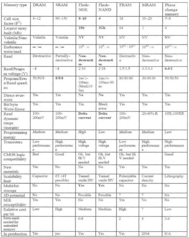
Table 1.1 Performance comparison between volatile memory (DRAM & SRAM) and nonvolatile memory (Flash, FRAM, MRAM and PCM). Flash memory exhibits the best performance except the disadvantages of high programming voltage and slow program/erase speed.
………...10
Table 2-1 Electron and hole barrier high for SiO2 and Si3N4
………...…28
Table 3-1 The split table of the special SONOS nonvolatile memoryFigure Captions
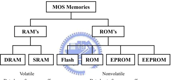
Figure1-1 MOS Memories Tree
………...…………11
Figure 1-2 Schematic cross section of the conventional floating gate nonvolatile memory device. Continuous poly-Silicon floating gate is used as the charge storage element.
………...………12
Figure 1-3 Schematic cross section of the SONOS nonvolatile memory device. The nitride layer is used as the charge-trapping element.
………13
Figure 1-4 The structure of the nanocrystal nonvolatile memory device. The semiconductor nanocrystals or metal nano-dots are used as the charge storage element instead of the continuous poly-Silicon floating
gate.
……….…14
Figure 2-1 Energy band diagram of MONOS.
………29
Figure 2-2 SONOS energy band diagram during retention mode
………30
Figure 2-3 Energy band diagram of SONOS structure with Si3N4 as the charge-storage layer during (a) program (write); and (b) erase
operations.
………31
Figure 2-4 (a) Positive gate voltage and positive drain voltage applied when use hot carrier injection to program (b) Energy band representation of hot carrier
Figure 2-5 (a) Positive gate voltage applied when use Fowler-Nordheim tunneling to program (b) Energy band representation of Fowler-Nordheim
tunneling
………...………33
Figure 2-6 The diagram of band to band hot electron injection
………..………34
Figure 2-7 The diagram of band to band hot hole injection
………34
Figure 2-8 Memory reading operation. The state “1” threshold voltage is low. The state “0” threshold voltage is high.
………35
Figure 2-9 The possible paths of charge loss during retention
………36
Figure 3-1 The SONOS nonvolatile memory device cross-section.
………46
Figure 3-2 The process flow of the nonvolatile memory devices.
………..47
Figure 3-3 ID-VG curves of the sample 2 nonvolatile memory device.
…………48
Figure 3-4 (a) Program and (b) Erase speed of Sample 1 nonvolatile memory device with different programming and erasing condition.
………..…49
Figure 3-5 (a) Program and (b) Erase speed of Sample 2 nonvolatile memory device with different programming and erasing condition.
…………..……50
Figure 3-6 (a) Program and (b) Erase speed of Sample 3 nonvolatile memory device with different programming and erasing condition.
…………..……51
Figure 3-7 (a) Program and (b) Erase speed of Sample 4 nonvolatile memory device with different programming and erasing condition.
………..…52
Figure 3-8 (a) Program and (b) Erase speed of Sample 5 nonvolatile memory device with different programming and erasing condition.
…………..……53
Figure 3-9 (a) Program and (b) Erase speed of nonvolatile memory devices for comparing different Si3N4 thickness.
………54
Figure 3-10 Endurance characteristics of the sample 1 memory device.
……...…55
Figure 3-11 Endurance characteristics of the sample 2 memory device.
……...…55
Figure 3-12 Endurance characteristics of the sample 3 memory device.
……...…56
Figure 3-13 Endurance characteristics of the sample 4 memory device.
……...…56
Figure 3-14 Endurance characteristics of the sample 5 memory device.
……...…57
Figure 3-15 Retention characteristics of the sample 1 memory device.
……….…58
Figure 3-16 Retention characteristics of the sample 2 memory device.
…….……58
Figure 3-17 Retention characteristics of the sample 3 memory device.
……….…59
Figure 3-18 Retention characteristics of the sample 4 memory device.
……….…59
Figure 3-19 Retention characteristics of the sample 5 memory device.
……….…60
Figure 3-20 Retention characteristics of the sample 2 and the sample 3 nonvolatile memory devices for comparing different temperature.
……….……60
Figure 3-21 Retention characteristics of the sample 1 memory device compare with fresh and 100K P/E cycles at 25℃.
………...…61
Figure 3-22 Retention characteristics of the sample 2 memory device compare with fresh and 100K P/E cycles at 25℃.
………...…61
Figure 3-23 Retention characteristics of the sample 3 memory device compare withfresh and 100K P/E cycles at 25℃.
………...…62
Figure 3-24 Retention characteristics of the sample 2 and sample 3 memory devicecompare with fresh and 100K P/E cycles at 25℃.
…………...……62
Figure 3-25 Drain disturbance characteristics of the flash memory devices in the (a)program state and (b) erase state.
………..……63
Figure 3-26 Gate disturbance characteristics of the flash memory devices in the (a) program state and (b) erase state.
………..…………64
Figure 3-27 Read disturbance characteristics of the flash memory devices in the (a) program state and (b) erase state.
………..………65
Chapter 1
Introduction
1-1 Background
The first semiconductor transistor is invented since 1960 ages. One of great invention is semiconductor memory. In the past decade, about 20% of semiconductor market is given by the semiconductor market, which can be approximately divided into two main categories: Random Access Memories (RAM’s) and Read Only Memories (ROM’s). The MOS memory tree was showed in Figure 1-1. Both are based on the complementary metal oxide semiconductor (CMOS) technology. The two kinds of memories are most different in data retention. Data will be reserved or said nonvolatile after power off named ROM, opposite one data will be lost or said volatile after power off named RAM. The volatile memories like DRAM or SRAM, that very dense and have fast speed in programming and reading. RAM is massive applied in computer industry. The nonvolatile memories like Flash, ROM, EPROM, or EEROM, are able to balance the loss-aggressive programming and reading performances with no volatility.
the electronic industries urgently needed a new kind of memory device to replace the magnetic-core memory. Today, Flash memories represent a considerable amount of the overall semiconductor memory market. Portable electronic products, such as cellular phone, digital camera, mobile PC, mp3 audio player, USB Flash personal disc, intelligent IC card, and so on, have widely applied. The wireless communication devices and semiconductor memories have also applied widely. These products are all based on nonvolatile memory. They have been the explosive growth of the Flash memory market. There are two major applications for Flash memories that should be pointed out. The first application is the possibility of nonvolatile memory integration in logic system-mainly and so on. The other application is to create storing elements, such as memory boards or solid-state hard disks. Solid-state disks are very useful for portable applications, since they have small dimensions, low power consumption, and no mobile parts, therefore being more robust. Flash combine the capability of nonvolatile storage with an access time comparable to DRAM’s, which allows direct execution of micro codes. Flash memories can find interesting applications in personal computer program management: many programs can be stored in Flash chips, without being continuously loaded and unloaded from hard disk partitions, and directly executed.
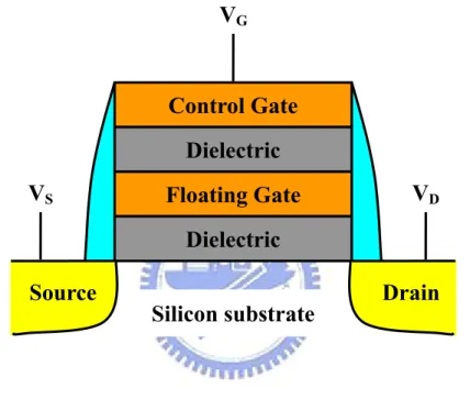
semiconductor memory at Bell Labs [1]. The FG structure device show in Figure 1-2. It has a poly-silicon gate completely surrounded by dielectric. The floating gate is electrically governed by a capacitive couple control gate (CG). The operation principal is using the polycrystalline silicon as FG to be the charge store units for the cell device. When electrons injected to the floating gate from channel, the threshold voltage of devices will be shifted. The logical “0”and “1” definition of nonvolatile memory devices is used that the difference between threshold voltage. Several physical mechanisms are available to accomplish this charge transfer, but the most commonly used ones are rather channel hot electron injection (CHEI) or Fowler-Nordheim (FN) tunneling for the write operation, and FN tunneling for the erase operation. A Flash memory cell is basically a floating-gate MOS transistor. Flash memory fabrication process is compatible with the current CMOS process and is a suitable solution for embedded memory applications. A Flash memory cell is simply a MOSFET cell, except that a poly-silicon floating gate is sandwiched between a tunnel oxide and an inter-poly oxide to form a charge storage layer [2].
Compared with DRAM, flash memory with floating gate structure ensures low power and long retention time and has much high array density. The stacked-gate FG device structure continues to be the most prevailing nonvolatile semiconductor memory (NVSM) implementation, and is widely used in both standalone and
embedded memories, and in both code and data storage applications. Although convention FG memories have many advantages over other kinds of nonvolatile memories, it still comes to be in face of their limitations from scaling down issues for the coming generation [3]. The most prominent limitation is the limited potential for continued scaling of the device structure. This scaling limitation stems from the extreme requirements put on the tunnel oxide layer. In general, the tunnel oxide has to enable quick and efficient charge transfer to and from the FG. Moreover, the tunnel oxide needs to provide superior isolation under retention, endurance, and disturbed conditions in order to maintain information integrity over periods of up to a decade. Once the tunnel oxide is made relatively thicker to provide superior isolation for retention, the program/erase speed will be slower and the operation voltage will be high. Uses the thinner tunnel oxide can resolve the problem above, but why we can’t use the thinner oxide as tunnel oxide? The reasons are that once the deterioration of the tunnel oxide has been created because of the high electric fields across isolator, the electrons stored in FG can tunnel back to channel, and since poly-silicon is a conducting material, once the tunnel oxide develops a leaky path under repeated program/erase operation, all the stored charge in the floating gate will be lost. In other words, when the tunnel oxide is thin enough to achieve the speed request, the retention characteristics may be degraded. As a result, there is a trade-off between
speed and retention. The thickness of the tunnel oxide is compromised to about 8-11nm, which is barely reduced over more than five successive generations of the industry [4]. Table 1.1 shows performance comparison between volatile memories and nonvolatile memories.
To overcome the scaling limits of the conventional FG structure for the coming generations, two candidates are mostly mentioned that are SONOS [5-7] and nanocrystal memories [8-10]. As for SONOS in Figure 1-3, the nitride layer is used as the charge-trapping element. The intrinsic distributed storage takes an advantage of the SONOS device over the FG device, its improved endurance, since a single defect will not cause the discharge of the memory [5]. Tiwari et al. [8] for the first time demonstrated the silcon nanocrystal floating gate memory device in the early nineties. As shown in Figure 1-4, the local leaky path will not cause the entire loss of information for the nanocrystal nonvolatile memory device. Also, the nanocrystal memory device can maintain good retention characteristics when tunnel oxide is thinner and lower the power consumption [8-10]. The term “endurance” refers to the ability of the NVSM to withstand repeated program cycles and still meet the specification in the data sheet. The term “retention” describes the ability of the NVSM to store and recover information after a number of program cycles at a specified temperature. The basic idea of the “discrete-trap” mechanism is to replace the floating
gate of nonvolatile memories by many discrete trapping centers, which can be made by natural traps in an appropriate insulator (for SONOS structure use nitride layer) or by semiconductor nanocrystals (usually silicon dot).The intrinsic distributed storage takes an advantage of SONOS device and nanocrystal device than the FG device, since a single defect will not cause the discharge of memory. Charge trapped in discrete trap centers are more immune to the leakage caused by localized oxide defects, thus allowing more aggressive scale down for the next generation.
1-2 Motivation
Since 1960 ages, there are two main technologies for the nonvolatile semiconductor memory. The one is floating gate structure. The other is metal-nitride-oxide-silicon (MONS) and polysilicon-blocking oxide-silicon nitride-tunneling oxide-silicon (SONOS) structure. The storage mediums are different for two nonvolatile memory structures. To the floating gate nonvolatile memory, the storage medium is poly-silicon, which is a conductor. The charge storage ability is dependent on the dielectric around poly-silicon. Since 1980 ages, Maserjian et al. [11] observe the leakage current increase under less than 7MV/cm electric field for thin oxide. The leakage current is so-called stress induced leakage current (SILC). As the devices scaling down trend, the floating gate nonvolatile memory structure is
insufficient due to the stress induce leakage current phenomenon cause the retention and endurance can not achieve the specifications for the ordinary nonvolatile semiconductor memories. The stress induced leakage current is thought the current through the oxide under high electric field result some traps produced. These traps make the electric conduction capability increase of the oxide because the traps assist the carrier through the dielectric (Trap-Assisted Tunneling, TAT). Hence, some people propose replacing SiO2 with oxynitrade [12-15]. Therefore, we use oxynitrade as the tunneling oxide because that the interface-trap density will increase at SiO2/Si interface during the program/erase for a nonvolatile memory. The other nonvolatile semiconductor memory structure is nitride base, which uses the trap of high density in the Si3N4 to catch charges. Therefore, the charge storage ability is not only dependent on the dielectric. Hence, the thickness of dielectric can be scaling down. Furthermore, the nitride base nonvolatile semiconductor memories improve the loss of the charge stored due to the radiation largely. Due to the shallow trap density is very high in the nitride, the electrons stored in the nitride jump by the trap easily, which is so-called hopping conduction. Therefore, we hope that the number of nitride traps is suitable. Some peoples use oxynitride as trapping layer because it can reduces the shallow trap density and have good endurance characteristics after 105 program/erase cycles. Due to the precursors of oxynitride have oxygen atom. The hydrogen will be replaced by
oxygen and produce the deep trap, which energy band analyzed is 2eV below the conduction band of silicon nitride. The reaction is expressed as:
2≣Si3N+2NOÆ2≣Si‧+2≣Si2O 2≣Si‧
+‧
≣SiÆ≣Si─Si≣
However, we will adopt reoxidation process after the silicon nitride trapping layer deposited to produce the amphoteric deep trap “≣Si─Si≣”, and it is effective to improve the data retention. Then, the energy band of blocking oxide connecting with nitride for the conventional SONOS structure is smooth. Hence, the holes tunnel easily across blocking oxide and it will harm the blocking oxide. However, S. Minami mentioned the energy band of blocking oxide connecting with nitride for using CVD TEOS oxide as blocking oxide is steep. The holes will not tunnel through blocking oxide easily, and that can improve the characteristics of data retention. So we adopt CVD TEOS as blocking oxide.
1-3 Organization of the Thesis
This dissertation is divided into four chapters. The contents in each chapter are described as follows:
In chapter 1, the potential memory devices about conventional floating gate and SONOS memory devices are introduced.
In chapter 2, the studied focus on the introduction of the basic principles of nonvolatile memory device.
In chapter 3, we describe the process flow for fabricating SONOS test devices. We will show some basic electrical characteristics between different methods and conditions.
Table 1.1
Performance comparison between volatile memory (DRAM
& SRAM) and nonvolatile memory (Flash, FRAM, MRAM and PCM).
Flash memory exhibits the best performance except the disadvantages of
Figure 1-1 MOS Memories Tree
MOS Memories
ROM’s
RAM’s
EEPROM
EPROM
ROM
Flash
SRAM
DRAM
VolatileData loss after power off
Nonvolatile Data kept after power off
Figure 1-2 Schematic cross section of the conventional floating gate
nonvolatile memory device. Continuous poly-Silicon floating gate is used
as the charge storage element.
Silicon substrate
Control Gate
Dielectric
Floating Gate
Dielectric
Source
Drain
V
GV
DV
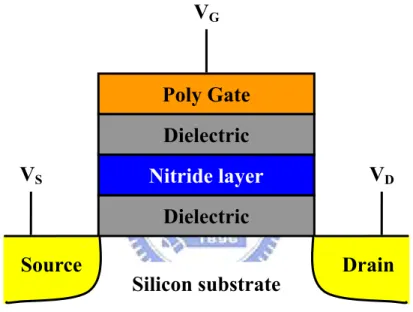
SFigure 1-3 Schematic cross section of the SONOS nonvolatile memory
device. The nitride layer is used as the charge-trapping element.
Silicon substrate
Poly Gate
Dielectric
Nitride layer
Dielectric
Source
Drain
V
GV
DV
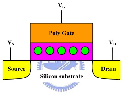
SFigure 1-4 The structure of the nanocrystal nonvolatile memory device.
The semiconductor nanocrystals or metal nano-dots are used as the
charge storage element instead of the continuous poly-Silicon floating
gate.
Silicon substrate
Poly Gate
Source
Drain
V
GV
DV
SChapter 2
Basic Principles of Nonvolatile Memory
2-1 Introduction
For the triple-dielectric poly-silicon / blocking oxide / silicon nitride / tunneling oxide / silicon (SONOS) structure nonvolatile memory, charge traps distributed throughout the block of the nitride layer. A typical trap has a density of the order 1018-1019 cm-3 according to Yang et al [17] and stores both electrons and holes injected from the channel. Here, SONOS structure is an attractive candidate for high density EEPROM’s suitable for semiconductor disks and as a replacement for high-density dynamic random access memories (DRAM’s). The nitride-based memory devices were extensively studied in the early 70s after the first metal-gate nitride device metal/nitride/oxide/silicon (MNOS) was reported in 1967 by Wegener et al [18]. SONOS nonvolatile semiconductor memories meet the challenges of scaling down issue. In general, nonvolatile semiconductor memories are required to bear 10K-100K times write/erase cycles (endurance) and have 10 years memory retention at the temperatures as high as 125℃. A tunnel oxide of 3nm is thick enough to guarantee 10 years retention time in the SONOS flash memory. The SONOS memory device has received a lot of attention due to its advantages over the
traditional FG memory device. These advantages include reduced process complexity, lower voltage operation, improved cycling endurance, and elimination of grain induced turn-on [19]. Low programming voltages and high endurance are possible in this multi dielectric technology as the intermediate Si3N4 layer is scaled to thicknesses of 50Å. Oxide thickness in this range is necessary to minimize the undesirable effects of gate disturb while still enabling a low-voltage operation to maximize the cost benefit of SONOS memories. The thin gate insulator and low programming voltage enable the scaling of the basic memory cell and associated complementary metal-oxide-semiconductor (CMOS) peripheral circuitry on the memory chip. Advancements in ultra-thin tunnel oxides during the 1990s have opened the path to improve performance and reliability for NVSMs based on SONOS technology [20]. The optimization of nitride and oxide films has been the main focus in recent years.
For SONOS nonvolatile semiconductor memories, the basics operating principle of ONO structure is that the electrons injected from the channel are trapped in the forbidden gap of the silicon nitride film during the program operation. Hence, the electrons can not move freely between the discrete trap locations. Therefore, the SONOS memory device is very robust against the defects inside the tunneling oxide and has better endurance than the floating gate flash memory. Because the electrons injected from the channel are trapped in poly-silicon conduction band for floating gate
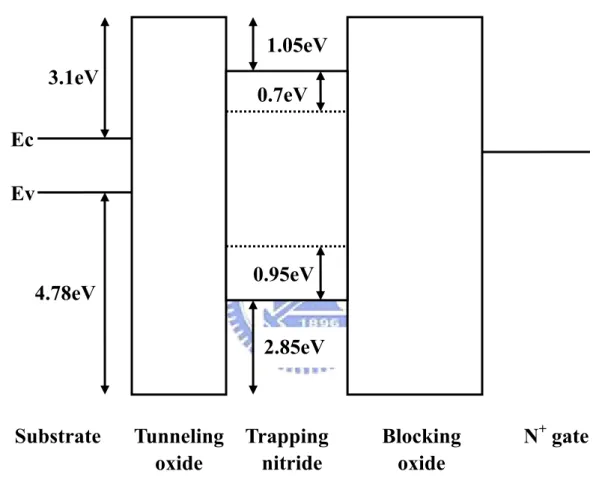
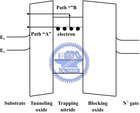
structure. On the other hand, holes are injected from the substrate into silicon nitride film. The relation between bias and energy band bending is importance to understand basics program and erase mechanisms. Figure 2-1 shows energy band diagram of MONOS. The barrier of SiO2 is about 3.1eV for electrons in the conduction band of silicon, and 4.78eV for holes in the valance band. The barrier of Si3N4 is about 1.05eV for electrons in the conduction band of nitride, and 2.85eV for holes in the valance band, the gap for electrons between conduction band and trapping level is 0.7eV, and for holes between valance band and trapping level is 0.95eV. The energy band diagram during retention is showed in Figure 2-2. In the retention mode, electrons can leak to the substrate through the direct tunneling process shown as path “A” in Figure 2-2. Alternatively, electrons can be thermally de-trapped into the nitride conduction band and then tunnel back to the channel, which is shown as path “B” in Figure 2-2. The thermal de-trapped rate is exponentially reduced with a deep trap energy level. Hence, the escape probability of electron trapped is very small. For these reasons, the SONOS flash memory can have much better retention time than the floating gate memory.
In this chapter, we will discuss program and erase mechanisms of SONOS memory devices from the relation between bias and energy band bending. Programming operations, such as Fowler-Nordheim tunneling and channel hot electron injection,
and erasing operations, such as band to band assisted hole injection and channel hot hole injection, will be discussed briefly. Channel hot-hole injection is mainly used in nonvolatile memory devices in erasing mechanism. Moreover, the reliability characteristic of data retention and endurance will also be discussed.
2-2 Program/Erase operation mechanisms
In the floating gate memories, four main physical mechanisms are introduced as follows: Fowler-Nordheim tunneling (FN), modified Fowler-Nordheim tunneling, trap-assisted tunneling, and channel hot-electron injection (CHE). The first three mechanisms are quantum-mechanical tunnel induced by an electric field. The CHE mechanism is that electrons gain enough energy to pass the oxide–silicon energy barrier, due to the electric field in the transistor channel between source and drain.
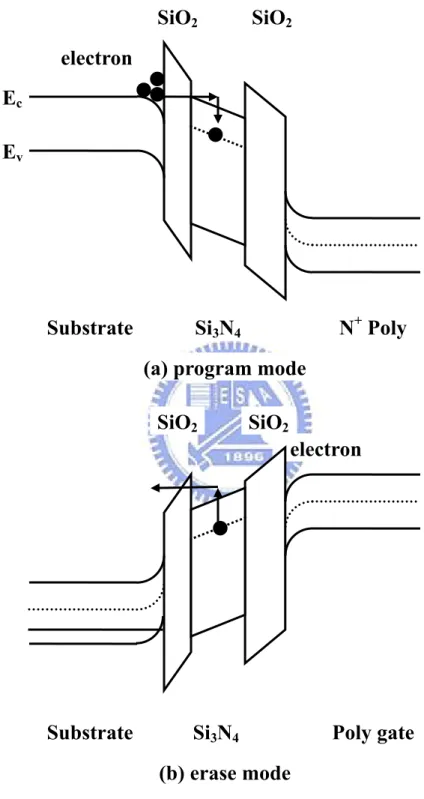
In SONOS type nonvolatile memory devices, Fowler-Nordheim tunneling (FN), band to band tunneling (BTBT), trap-assisted tunneling (TAT), and modified Fowler-Nordheim tunneling mechanisms (MFN) are the main programming mechanisms [21]. For SONOS structure, the program and erase processes for an n-channel semiconductor memory device are illustrated schematically in Figure 2-3. During the program process, a positive gate voltage is applied to inject channel inversion-layer electrons into the nitride layer. During the erase process, a reverse gate
voltage is applied to cause the electrons to tunnel back into the channel and the accumulation layer holes to tunnel into the nitride film from the substrate.
There are many methods to achieve “programming” or “erasing”. In general, hot carrier electron injection and Fowler-Nordheim tunneling are most utilized to program and erase the novel nonvolatile memories. In this section, these operation mechanisms will be described in detail.
2-2.1 Channel Hot Electron injection (CHEI)
During programming, the positive voltages applied to the gate and drain while the source is grounded. These voltages generate a lateral and vertical electric field along the channel. At low fields, this is a dynamic equilibrium condition, which holds until the field strength reaches approximately 100kV/cm [22]. For fields exceeding this value, electrons are no longer in equilibrium with the lattice. The electrons will move from the source to the drain and be accelerated by the lateral field near the drain junction in the channel. Electrons are “heated” by the lateral electric field, and a small fraction of them have enough energy to overcome the barrier between oxide and silicon conduction band edges. Once the electrons gain enough energy, they can surpass the energy barrier of the oxide layers and inject into trapping layer and be trapped, which is the so-called hot-carrier injection gate current. The current density
) exp( ) ( 2 m b b m ds d inj E E I A I λ ϕ ϕ λ − = (2-1)
Figure 2-4 shows the phenomenon of hot electron injection. This mechanism is schematically represented for the case of an n-channel nonvolatile memory. To distinguish from Fowler-Nordheim tunneling, the definition of hot carrier injection in this study is the only condition that the drain is applied bias.
2-2.2 Fowler–Nordheim Tunneling (F-N tunneling)
Tunneling is another way to program electrons into nitride layer from the substrate. But electrons could also tunnel back to the channel during retention, constituting a large leakage current. The magnitude of the leakage current depends on both the thickness and the electron barrier height of the tunneling dielectric. The tunneling probability is expressed in Equation 2-2.
⎟ ⎟ ⎠ ⎞ ⎜ ⎜ ⎝ ⎛ − =
∫
d e dx m x T 0 * ) ( 2 exp h φ (2-2)Hereφ(x)is barrier height. It is 3.1eV in Si-SiO2 for electrons see Table 2.1[23-27].
d is tunneling dielectric thickness, h is the Planck’s constant and m is the e
electron mass inside the tunneling dielectric and it is 0 m for both nitride and .5 0 oxide.
its band structure will be influenced as indicated in Figure 2-5. The Fowler-Nordheim tunneling mechanism occurs when applying a strong electric field (in the range of 8–10MV/cm) across a thin oxide. In these conditions, the energy band diagram of the oxide region is very steep. Electrons in the p-type substrate conduction band transfer from trapezoidal to triangular energy barrier. Therefore, there is a high probability of electrons passing through the energy barrier itself. A significant tunnel current can be observed when the tunnel oxide thickness is less than 4nm. The Fowler-Nordheim tunneling current related formula is shown in Equation 2-3.
⎥ ⎥ ⎥ ⎦ ⎤ ⎢ ⎢ ⎢ ⎣ ⎡ − = qhE q m E J e b 3 ) ( 2 8 exp 2 3 2 π φ (2-3)
Here E is the electric field which is defined as the applied voltage divide by total thickness of the tunneling oxide and the blocking oxide. When the voltage drop across the tunneling dielectric exceeds the electron tunneling barrier height, Fowler-Nordheim tunneling current depends on the tunneling barrier height than on the tunneling dielectric thickness. Increasing the tunneling dielectric thickness will not decrease the tunneling current if the same electric field is applied.
2-2.3 Modified Fowler–Nordheim Tunneling
Fowler-Nordheim tunneling mechanism, yet the carriers enter the nitride at a distance further from the tunnel oxide-nitride interface. MFN mechanism is frequently observed in SONOS memories. The SONOS memory is designed for low-voltage operation (<10V, depending on the Equivalent oxide thickness), a relatively weak electrical field couldn’t inject charges by direct tunneling or FN mechanism.
2-2.4 Direct Tunneling
For SONOS memories, the control-gate coupling ratio of SONOS memory devices is inherently small. As a result, Fowler-Nordheim tunneling cannot serve as an efficient program/erase mechanism when a relatively thick tunneling oxide is used, because the strong electric field cannot be confined in one oxide layer. The direct tunneling is employed in SONOS memories instead. In the other hand, the direct tunneling is more sensitive to the barrier width than barrier height, two to four orders of magnitude reduction in leakage current can still be achieved if large work function metals, such as Au or Pt.
2-2.5 Band to Band Tunneling (BTBT)
Band to band tunneling application to nonvolatile memory was first proposed in 1989. I. C. Chen and et al. demonstrated a high injection efficiency (about 1%) method to programming EPROM devices [29]. Band-to-band Tunneling (BTBT)
process occurs in the deeply depleted doped surface region under the gate to drain / gate to source overlap region. In this condition, the band-to-band tunneling current density is expressed in Equation 2-4.
⎥ ⎥ ⎥ ⎦ ⎤ ⎢ ⎢ ⎢ ⎣ ⎡ − = − h h ε π q E m E V q m J g g app b b 3 * 2 4 exp 4 * 2 2 3 2 1 2 3 3 (2-4)
(a) Band to Band Hot Electron Tunneling Injection
When band-bending is higher than the energy gap of the semiconductor, the tunneling electron from the valence band to the conduction band becomes significant. The mechanism is at the condition for positive gate voltage and negative drain voltage. Hence, the hot electrons are injected through the tunnel oxide and then recombine the stored electrons as shown in Figure 2-6.
(b) Band to Band Hot Hole Tunneling Injection
The injection is applied for p-type nonvolatile memory device. The mechanism is
at the condition for negative gate voltage and positive drain voltage. Hence, the hot holes are injected through the tunnel oxide and then recombine the stored electrons as shown in Figure 2-7.
2-2.6 Trap Assistant Tunneling
The charge storage mediums with many traps may cause another tunneling mechanism. For example, the charges tunnel through a thin oxide and arrive to the
traps of nitride layer at very low electrical field in SONOS systems. During trap assisted injection the traps are emptied with a smaller time constant then they are filled. The charge carriers are thus injected at the same distance into the nitride as for MFN injection. Because of the sufficient injection current, trap assistant tunneling may influence in retention [30].
2-3 Reading operation
The data stored in a Flash cell can be determined measuring the threshold voltage of the memories. When electrons stored in trapping layer, the threshold voltage will shift (△VT) that is proportional to the stored electron charge (Q). The threshold voltage shift of a Flash transistor can be written in Equation 2-5 [31-32].
C Q
VT =−
∆ (2-5) Here Q is the charge stored in trapping layer, and C is the capacitance between trapping layer and control gate. The threshold voltage of the memory cell can be altered by changing the amount of charge present between the gate and the channel, corresponding to the two states of the memory cell, i.e., the binary values (“1” and “0”) of the stored bit. If there are charges stored in the silicon nitride film, the threshold voltage can be modified to switch between two distinct values [33]. Figure 2-8 shows the threshold voltage shift between two states in a flash memory. To a
nonvolatile memory, it can be “written” into either state “1” or ”0” by either “programming” or “erasing” methods, which are decided by the definition of memory cell itself.
2-4 Nonvolatile Memory Device reliability
Retention, endurance, and disturb experiments are performed to investigate Flash-cell reliability.
2-4.1 Retention
In any nonvolatile memory technology, it is essential to retain data for over ten years. This means the loss of charge stored in the storage medium must be as minimal as possible. For SONOS memory devices, data are represented as electrons stored in the silicon nitride layer, the stored charges leak away from the trapping layer through the tunnel oxide or through the inter-poly dielectrics, and the lateral migration of charges trapped in the silicon nitride layer [34-35]. For example, in modern Flash cells, FG capacitance is approximately 1fF. A loss of only 1fC can cause a 1V threshold voltage shift. Possible causes of charge loss are: 1) by tunneling emission mechanism; 2) thermionic emission mechanism; 3) defects in the tunnel oxide; and 4) de-trapping of charge from insulating layers surrounding the storage medium.
electrons trapped can tunnel back to the conduction band of the silicon substrate (trap to band tunneling, TBT) and the Si and SiO2 interface traps (trap to trap tunneling, TTT) under the influence of an internal self-built electric field, or loss to the conduction band of the silicon nitride by thermal energy and then tunnel to silicon substrate by the lateral electric field (thermal assist tunneling, TAT). Meanwhile, holes from the substrate may tunnel through the thin tunneling oxide and become trapped in the nitride (band to trap tunneling, BTT). The retention capability of Flash memories has to be checked by using accelerated tests that usually adopt screening electric fields and hostile environments at high temperature.
2-4.2 Endurance
Endurance is the number of program/erase operations that the memory will complete and continue to operate as specified in the data sheet. In a conventional flash memory the maximum number of program/erase cycles that the device must sustain more than 105. The program/erase cycle usually used the Fowler-Nordheim tunneling or channel hot electron injection mechanism under room temperature environment. As the experiment was performed applying constant pulses, the variations of program and erase threshold voltage levels are described as “program/erase threshold voltage window closure” and give a measure of the tunnel oxide aging [37-38]. In particular,
the oxide and interface state generation at the drain side of the channel. The evolution of the erase threshold voltage reflects the dynamics of net fixed charge in the tunnel oxide as a function of the injected charge. The initial lowering of the erase is due to a pile-up of positive charge which enhances tunneling efficiency, while the long-term increase of the erase is due to a generation of negative traps. The endurance characteristics give the memory threshold voltage window, which is the difference between the threshold voltages in the programmed state and the erased states. It is the parameters to describe how good the reliable is a nonvolatile memory cell.
2-5 Summary
Good data retention and endurance and less disturb are an important issue of the SONOS type nonvolatile memory device. These issues affect the scalability of thin dielectric such as tunneling oxide thickness. Therefore, the SONOS nonvolatile memory with re-oxidation is proposed to enhance nonvolatile memory reliability. It’s includes both retention and endurance issue.
Tunneling layer Electron barrier (eV) Hole barrier (eV) SiO2 3.15 4.7 SiN 2.4 1.8 Al2O3 2.9 4.3 HfO2 1.6 3.3 Ta2O5 0.3 3.0
Figure 2-1 Energy band diagram of MONOS.
2.85eV
3.1eV
4.78eV
0.95eV
0.7eV
1.05eV
Tunneling
oxide
Blocking
oxide
Trapping
nitride
Ec
Ev
Substrate
N
+gate
Figure 2-2 SONOS energy band diagram during retention mode
Path “”B
electron
Path “A”
Tunneling
oxide
Blocking
oxide
Trapping
nitride
E
cE
vSubstrate
N
+gate
Figure 2-3 Energy band diagram of SONOS structure with Si3N4 as the
charge-storage layer during (a) program (write); and (b) erase operations.
electron
electron
Substrate
Si
3N
4N
+Poly
SiO
2SiO
2SiO
2SiO
2Si
3N
4Poly gate
Substrate
(a) program mode
(b) erase mode
E
cFigure 2-4 (a) Positive gate voltage and positive drain voltage applied
when use hot carrier injection to program (b) Energy band representation
of hot carrier injection
electron
Silicon substrate
Control Gate
Dielectric
Floating Gate
Dielectric
N
+N
+V
G>0V
V
D>0V
V
S=0V
electron
Substrate
Si
3N
4N
+Poly
SiO
2SiO
2E
cE
v(a)
(b)
Figure 2-5 (a) Positive gate voltage applied when use Fowler-Nordheim
tunneling to program (b) Energy band representation of Fowler-Nordheim
tunneling
Silicon substrate
Control Gate
Dielectric
Dielectric
N
+N
+V
G>0V
V
D=0V
V
S=0V
electron
Substrate
Si
3N
4N
+Poly
SiO
2SiO
2E
cE
v(a)
(b)
Floating Gate
Figure 2-6 The diagram of band to band hot electron injection
Figure 2-7 The diagram of band to band hot hole injection
Silicon substrate
Control Gate
Dielectric
Dielectric
N
+N
+V
G<0V
V
D>0V
V
S=0V
Floating Gate
Silicon substrate
Control Gate
Dielectric
Dielectric
P
-P
-V
G>0V
V
D<0V
V
S=0V
Floating Gate
0 1 2 3 4 5 10-10 10-9 10-8 10-7 10-6 10-5 10-4 10-3 Vth shift ID ( A ) VG (V) Neutral state "1" Charge state "0"
Figure 2-8 Memory reading operation. The state “1” threshold voltage is
low. The state “0” threshold voltage is high.
Figure 2-9 The possible paths of charge loss during retention
electron
Tunneling
oxide
Trapping
nitride
Substrate
hole
BTT
TTT
TBT
TAT
Chapter 3
Experiment Process and
Characterization
3-1 Experimental
Figure 3-1 shows the SONOS nonvolatile memory device cross-section. Figure 3-2 schematically describes the process flow of the nonvolatile memory devices. The split table shows in the Table 3-1. For manufacture nonvolatile memory devices, we carried out on 6-inch p-type (100)-oriented silicon wafer with a resistivity of 15-25Ω-cm. the fabrication process of these memory devices was started with LOCOS isolation process. Wafers were cleaned using standard RCA cleaning. The wafers were dipped in diluted HF solution to remove native oxides before growing the chemical oxide film. Subsequently, the wafers were immediately immersed into H2O2 solution at room temperature for 20 min to grow 10Ǻ chemical oxide [39]. The chemical oxide was nitrified by LPCVD in low-pressure (180mTorr) NH3 ambient at 780℃ for 14 min. After that, the chemical oxynitride was placed in atmospheric O2 ambient at 923℃ for 15min. Then, 30Ǻ, 50Ǻ , and 80Ǻ silicon nitride was deposited by furnace system in NH3 and SiH2Cl2 ambient at 780℃ individually. Only the sample 3 nonvolatile memory device is re-oxidation in atmospheric O2 ambient at
923℃ for 15min. Furthermore, about 100Ǻ blocking oxide was deposited by LPCVD in low-pressure (about 300mTorr) Tetra-Ethyl-Ortho-Silicate (TEOS) ambient at 700℃. After CVD TEOS was deposited, we placed these wafers in atmospheric O2 at 923℃ for 15min to densify. A 200nm-thick poly-silicon was deposited succeeding by LPCVD to serve as gate electrode. Subsequently, gate patterning, source/drain implanting, and the remaining standard CMOS procedures were completed to fabricate the special SONOS nonvolatile memory devices.
3-2 Result and Discussion
In this thesis, all devices described had dimensions of L/W = 0.5/10 µm, and the threshold voltage (Vth) is defined when the ID current reach 10-7A in ID-VG curves. The electrical characteristics of the special SONOS nonvolatile memory devices are measurement by HP4156C Precision Semiconductor Parameter Analyzer and HP41501A Pulse Generater.
3-2.1 Characteristics of Flash Devices
Figure 3-3 shows the ID-VG curve of the sample 2 nonvolatile memory device under fresh, programmed, and erased states. Channel hot-electron injection and band-to-band hot-hole injection were employed for programming and erasing respectively. The programming and erasing time are both 10ms, and a memory
window of about 2V can be clearly observed. During programming, a small fraction of electrons in the substrate obtain enough energy from applied voltage VD to surmount the barrier between oxide and silicon conduction band edges. There electrons can be trapped in silicon nitride layer and the threshold voltage shift to right. When erasing, we applied a positive drain voltage VD to generate hot hole in the subject and a large enough negative gate voltage to across the energy barrier. It reduces the threshold voltage and causes the ID-VG curve shift to right. We use this mechanisms of adjust threshold voltage by different applied voltages to obtain memory characteristics.
The program and erase speed are shown in Figure 3-4, Figure 3-5, Figure 3-6,Figure 3-7, and Figure 3-8 for the different samples respectively. The “Vth shift” is defined as threshold voltage difference between the program state and erase state. Gate and drain terminals were biased equally from 7V to 9V. Both source and substrate were biased at 0V. As shown in Figure 3-4(a), Figure 3-5(a), Figure 3-6(a), Figure 3-7(a), and Figure 3-8(a), program characteristics as a function of pulse width. With VG and VD increasing, the Vth shift increases and the program speed becomes faster. The program time can be short as 10ms and a memory window of about 2V can be achieved for VG = VD = 8V. Figure 3-4(b), Figure 3-5(b), Figure 3-6(b), Figure 3-7(b), and Figure 3-8(b) show the erase characteristics of these special SONOS
nonvolatile memory devices for different conditions: VG = -6V, -7V, and -8V with the same VD = 7V. We can easily find similar phenomenon like programming, the Vth decrease faster as the applied gate voltage be more negative biased. The erase time was showed about 0.001s to 0.1s for different devices under VG = -7V and VD = 7V. A more important thing must be mentioned, there is that over-erase situation took place because the valance band of silicon nitride is higher than other storage medium, such as HfAlO [40]. Figure 3-9 shows the program and erase speed of nonvolatile memory devices for comparing different silicon nitride thickness. Under the same programming or erasing bias, the thicker silicon nitride has faster program speed and erase, because the thicker trapping layer causes the total capacitance between the poly-gate and substrate becomes smaller, then the electric field will become large.
The endurance characteristics after 105 program/erase cycles of these sample nonvolatile memory devices are shown in Figure 3-10, Figure 3-11, Figure 3-12, Figure 3-13, and Figure 3-14. The programming and erasing conduction are approximately VG = VD = 8V for 10ms and VG = -7V, VD = 7V for 10ms. Small amount increase of the threshold voltages in programmed and erased state can be observed. This may be the stress-induced electron traps generated in the tunneling oxide during program/erase cycling [41]. For another reason, this is due to the mismatch between the localized spatial distributions for injected electron and holes by
using channel hot-electron programming and band-to-band hot-hole erasing. The uncompensated electrons cause to increase the threshold voltage in erase state over program/erase cycling.
Figure 3-15, Figure 3-16, Figure 3-17, Figure 3-18, and Figure 3-19 illustrate the retention characteristics of the nonvolatile memory devices for comparing different samples respectively. Furthermore, the quality of the tunneling oxide and the nitride trapping layer plays a significant role in charge retention. We can observe the densify of the blocking oxide is necessary to maintain a good characteristics of retention from comparing the Figure 3-18 and Figure 3-19. After that, we will discuss the effect of temperature factor for the sample 2 and sample 3. Figure 3-20 shows the retention characteristics of the sample 2 and the sample 3 nonvolatile memory devices for comparing different temperature (T = 25℃ and 125℃). It’s a pity that the retention go worst as the temperature increased [42-46]. However, it is notable that the data retention of sample 2 nonvolatile memory device is better than the sample 3. This indicates the re-oxidation procedure after the silicon nitride trapping layer deposited is a success way to improve the retention characteristics of the nonvolatile memories. The retention after program/erase cycles is also an important issue for flash memory. Because the retention of sample 4 and sample 5 nonvolatile memory devices had lose electrons trapped by silicon nitride trapping layer seriously, we discuss only the
retention characteristics of sample 1, sample 2, and sample 3 nonvolatile memory devices after endurance measurement. Figure 3-21, Figure 3-22, and 3-23 show the retention characteristics compare with fresh and 100K program/erase cycled at 25℃. We can find that the charge loss behavior of the devices with 100K cycling is more serious than the other. This means the tunneling oxide damaged after 100K program/erase cycling, thus stress-induced electron trapping in the tunneling oxide increases and the charge storage capability decreases, the retention characteristics go worst. Figure 3-24 shows the retention characteristics of the sample 2 and sample 3 memory devices compare with fresh and 100K program/erase cycles at 25℃ together. It is easy to observe the retention characteristics of the sample 3 memory device are better than the sample 2 memory device.
3-2.2 Disturbance Measurement
Figure 3-25 shows the programming and erasing drain disturbance characteristics of these sample nonvolatile memory devices. Drain disturbance may influence programmed memory to reduce the threshold voltage during programming. In this measurement, the VD = 6V and VG = VS = VB = 0V were applied in the programming and erasing drain disturbance measurement at room temperature 25℃.
threshold voltage. While a cell is being programmed, gate disturbance may occur for the cells sharing a common word line. The applied gate voltage attracts electrons in the substrate to tunnel to the silicon nitride, thus induce the threshold voltage to shift rightward. In this measurement, the VG = 6V and VD = VS = VB = 0V were applied to simulate the program situation which the cell unselected.
Figure 3-27 shows the read disturb characteristics in the program and erase states. There are two major factors causing the threshold voltage instability: the voltage of the word line and the bit line. The word line voltage during reading may enhance room temperature drift in the neighbor bit, and the bit line voltage during reading may cause unwanted channel hot electron injection and result in the threshold voltage shift subsequently. In this measurement, the gate voltage and drain voltage were applied at 3V and 0.5V respectively, then the source and the substrate voltage were grounded. No apparent read disturbance is observed for samples after stressing 1000s at 25℃.
3-3 Summary
In this chapter, we have investigated these memories effects and performances of the special SONOS nonvolatile memory devices. The re-oxidation process after silicon nitride deposited will improve the retention of nonvolatile flash memories. The energy band of the traps in the silicon trapping layer will be adjusted to suitable depth.
The desify of the TEOS blocking oxide is necessary to get a good reliability of the nonvolatile flash memory. The process we proposed is compatible with CMOS manufacturing technology of semiconductor industry.
Sample
Process
Sample 1 Sample 2 Sample 3 Sample 4
Sample 5
Tunneling
Oxide
18Ǻ SiON
Si
3N
4Trapping
Layer
30Ǻ 50Ǻ
50Ǻ
80Ǻ
80Ǻ
Re-oxidation
ˇ
Blocking
Oxide
100Ǻ CVD TEOS
Densify
ˇ
ˇ
ˇ
ˇ
Table 3-1 the split table of the special SONOS nonvolatile memory
devices.
Figure 3-1 The SONOS nonvolatile memory device cross-section.
Silicon substrate
Poly Gate
Blocking Oxide
Silicon Nitride
Tunneling Oxide
Source
Drain
LOCOS LOCOS
Figure 3-2 The process flow of the nonvolatile memory devices.
LOCOS
18Ǻ oxynitride
30Ǻ, 50Ǻ, 80Ǻ silicon nitride
100Ǻ CVD TEOS
Remain CMOS Procedures
Re-oxidation
Densify
Gate Pattern
0 1 2 3 4 5 10-14 10-13 10-12 10-11 10-10 10-9 10-8 10-7 10-6 10-5 10-4 10-3 10-2 ID-VG curves I D (A ) VG (V) fresh program erase Vth shift 2V
10-7 10-6 10-5 10-4 10-3 10-2 10-1 100 0 1 2 3 4 5 0 1 2 3 4 5 Sample 1 V G=VD=7V V G=VD=8V V G=VD=9V Program speed V th sh ift (V) Time (sec)
(a)
10-7 10-6 10-5 10-4 10-3 10-2 10-1 100 -0.5 0.0 0.5 1.0 1.5 2.0 2.5 -0.5 0.0 0.5 1.0 1.5 2.0 2.5 Erase speed V th s h ift (V ) Time (sec) Sample 1 VG=-6V;VD=7V VG=-7V;VD=7V VG=-8V;VD=7V(b)
10-7 10-6 10-5 10-4 10-3 10-2 10-1 100 0 1 2 3 4 5 0 1 2 3 4 5 Sample 2 V G=VD=7V V G=VD=8V V G=VD=9V Program speed V th sh ift (V) Time (sec)
(a)
10-7 10-6 10-5 10-4 10-3 10-2 10-1 100 -1.0 -0.5 0.0 0.5 1.0 1.5 2.0 2.5 -1.0 -0.5 0.0 0.5 1.0 1.5 2.0 2.5 Erase speed Sample 2 VG=-6V;VD=7V VG=-7V;VD=7V VG=-8V;VD=7V V th s h ift (V ) Time (sec)(b)
10-7 10-6 10-5 10-4 10-3 10-2 10-1 100 0 1 2 3 4 5 0 1 2 3 4 5 Sample 3 V G=VD=7V V G=VD=8V VG=VD=9V Program speed V th shi ft (V) Time (sec)
(a)
10-7 10-6 10-5 10-4 10-3 10-2 10-1 100 -1.5 -1.0 -0.5 0.0 0.5 1.0 1.5 2.0 2.5 -1.5 -1.0 -0.5 0.0 0.5 1.0 1.5 2.0 2.5 Erase speed Sample 3 VG=-6V;VD=7V VG=-7V;VD=7V VG=-8V;VD=7V V th s h ift (V ) Time (sec)(b)
10-7 10-6 10-5 10-4 10-3 10-2 10-1 100 0 1 2 3 4 5 0 1 2 3 4 5 Program speed Sample 4 VG=VD=7V V G=VD=8V VG=VD=9V V th shift (V ) Time (sec)
(a)
10-7 10-6 10-5 10-4 10-3 10-2 10-1 100 -2.5 -2.0 -1.5 -1.0 -0.5 0.0 0.5 1.0 1.5 2.0 2.5 -2.5 -2.0 -1.5 -1.0 -0.5 0.0 0.5 1.0 1.5 2.0 2.5 Erase speed Sample 4 VG=-6V;VD=7V VG=-7V;VD=7V VG=-8V;VD=7V V th s h ift (V ) Time (sec)(b)
10-7 10-6 10-5 10-4 10-3 10-2 10-1 100 0 1 2 3 4 5 0 1 2 3 4 5 Program speed Sample 5 V G=VD=7V V G=VD=8V V G=VD=9V V th sh ift (V) Time (sec)
(a)
10-7 10-6 10-5 10-4 10-3 10-2 10-1 100 -2.5 -2.0 -1.5 -1.0 -0.5 0.0 0.5 1.0 1.5 2.0 2.5 -2.5 -2.0 -1.5 -1.0 -0.5 0.0 0.5 1.0 1.5 2.0 2.5 Erase speed Sample 5 VG=-6V;VD=7V VG=-7V;VD=7V VG=-8V;VD=7V V th s h ift (V ) Time (sec)(b)
10-7 10-6 10-5 10-4 10-3 10-2 10-1 100 0 1 2 3 4 5 0 1 2 3 4 5 V D=VG=8V Sample 1 Sample 2 Sample 4 Program speed V th sh ift (V) Time (sec)
(a)
10-6 10-5 10-4 10-3 10-2 10-1 100 -2.5 -2.0 -1.5 -1.0 -0.5 0.0 0.5 1.0 1.5 2.0 2.5 -2.5 -2.0 -1.5 -1.0 -0.5 0.0 0.5 1.0 1.5 2.0 2.5 Erase speed VG=-8V;VD=7V Sample 1 Sample 2 Sample 4 V th s h ift (V ) Time (sec)(b)
100 101 102 103 104 105 0.0 0.5 1.0 1.5 2.0 2.5 3.0 3.5 4.0 0.0 0.5 1.0 1.5 2.0 2.5 3.0 3.5 4.0 Endurance Sample 1 Program Erase V th (V) P/E cycles
Figure 3-10 Endurance characteristics of the sample 1 memory device.
100 101 102 103 104 105 0.0 0.5 1.0 1.5 2.0 2.5 3.0 3.5 4.0 0.0 0.5 1.0 1.5 2.0 2.5 3.0 3.5 4.0 Endurance Sample 2 Program Erase V th (V) P/E cycles
100 101 102 103 104 105 0.0 0.5 1.0 1.5 2.0 2.5 3.0 3.5 4.0 0.0 0.5 1.0 1.5 2.0 2.5 3.0 3.5 4.0 Endurance Sample 3 Program Erase V th (V) P/E cycles
Figure 3-12 Endurance characteristics of the sample 3 memory device.
100 101 102 103 104 105 0.0 0.5 1.0 1.5 2.0 2.5 3.0 3.5 4.0 0.0 0.5 1.0 1.5 2.0 2.5 3.0 3.5 4.0 Endurance Sample 4 Program Erase V th (V) P/E cycles
100 101 102 103 104 105 0.0 0.5 1.0 1.5 2.0 2.5 3.0 3.5 4.0 0.0 0.5 1.0 1.5 2.0 2.5 3.0 3.5 4.0 Endurance Sample 5 Program Erase V th (V) P/E cycles
![HPSH [ 氧化數平衡反應式係數 ]](data:image/gif;base64,R0lGODlhAQABAIAAAP///wAAACH5BAEAAAAALAAAAAABAAEAAAICRAEAOw==)