行政院國家科學委員會補助專題研究計畫
□ 成 果 報 告
▓ 期中進度報告
單相切換式整流器無電流感測控制
之電壓迴路設計
Design of Voltage Loop in Current Sensorless Control
for Single-Phase Switch-Mode Rectifiers
計畫類別:▓ 個別型計畫 □ 整合型計畫
計畫編號:NSC98-2221-E-009-180-MY2
執行期間: 98 年 8 月 01 日至 100 年 07 月 31 日
計畫主持人:陳鴻祺 國立交通大學 電控工程研究所
成果報告類型(依經費核定清單規定繳交):▓精簡報告 □完整報告
本成果報告包括以下應繳交之附件:
□赴國外出差或研習心得報告一份
□出席國際學術會議心得報告及發表之論文各一份
□國際合作研究計畫國外研究報告書一份
處理方式:除產學合作研究計畫、提升產業技術及人才培育研究計畫、
列管計畫及下列情形者外,得立即公開查詢
▓涉及專利或其他智慧財產權,▓一年□二年後可公開查詢
執行單位:國立交通大學 電機與控制工程學系
中 華 民 國 99 年 5 月 6 日
單相切換式整流器無電流感測控制之電壓迴路設計
摘要-本兩年期計畫使用考量單相昇壓型切換式整流 器電路特性,研究設計應用於無電流感測控制之電壓迴路 設計。第一年計畫主要針對單相昇壓型切換式整流器電路 特性分析,考量參數不確定性對於切換式整流器控制性能 的影響,並提供模擬與實作結果加以驗證。 關鍵字:無電流感測控制Abstract- This two-year project is focused on the
design of voltage loop in the current sensorless control based on the behavior of the switched-mode rectifier. In the first year, the parameter uncertainty effect on the performance of SMR is studied and simulation and experimental result are provided to demonstrate the derived equivalent model.
Keywords: current sensorless control
I.SINGLE-LOOPCURRENT
SENSORLESSCONTROL(SLCSC)
A. Boost-Type SMR
As shown in Fig. 1, the power circuit of the boost-type SMR mainly consists of a diode bridge rectifier and a boost-type DC/DC converter. When the switch SW is turning on, the input current flows through two rectifier diodes and the inductor L, and returns to the source. Similarly, the input current flows through two rectifier diodes, inductor L, and diode D and returns to the source when the power switch SW is turning off.
Due to the boost-type topology, the inductor current must be either positive or clamped to zero (i.e. no negative current). In steady state, the inductor current must be periodic with each half line cycle and can be expressed as a sum of infinite base current waveform
) 2 / (t nT iLn − ∑ − = =+∞ −∞ = n n Ln L T n t i t i ) 2 ( ) ( (1)
where T is the period of input line cycle and
(2) ) 0 ( ) 2 / ( Ln Ln T i i =
From the circuit topology shown in Fig. 1, the input current s is equal to positive inductor current L and negative inductor current when the input voltage
sp
s is positive and negative, respectively. Therefore, the input current can be represented [10] by i i L i − ) sin( t V v = ω (3) ) ( )) (sin( ) ( )) ( ( ) ( t i t sign t i t v sign t i L L s s ω = =
where is the sign operator and is defined as sign(•) (4) ⎩ ⎨ ⎧ < − ≥ + = 0 , 1 0 , 1 ) ( X when X when X sign
In order to model the behavior of a boost-type SMR simply, some assumptions are initially made:
(i) Power switch SW is assumed to operate at a switching frequency approaching infinity.
(ii) The small phase signal θ≈0 in radians is assumed and it follows that the approximations sinθ ≈θ and cosθ≈1
can be used.
(iii) A bulk capacitor d is assumed in the power circuit which contributes to the steady-state output voltage equal to voltage command . C d V * d
(iv) Both nominal sums of the conduction voltages in the loop of “switch SW on” and “switch SW off” are assumed to be equal to .
V
F
V
B. SLCSC
The configuration of the proposed SLCSC with the only voltage loop is plotted in Fig. 3. Like DPC in Fig. 2, the duty signal T is also generated from the comparison between a fixed triangle signal tri at (+) terminal and a control signal cont at (-) terminal and the output of voltage controller is a phase signal
G v
v
θ . To compensate the effect of inductor resistance and conducting voltages on the input current waveform, the control signal
in SLCSC is obtained by: cont v ] ˆ ) sin( ˆ ˆ ) sin( [ * sp F L d sp cont V V t L r t V V v = − − ω − ω θ θ ω (5)
where L and represent the nominal circuit values and VF is the sum of all the nominal conduction voltages.
rˆ Lˆ
ˆ
The differences between nominal values and real values can be represented as
L L L r r r = − ∆ ˆ (6) L L L= − ∆ ˆ (7) (8) F F F V V V = − ∆ ˆ
where L and are the real values in the boost-type SMR and VF is the sum of the real conduction voltages. With assumed infinite switching frequency, the average duty ratio signal
r L
d over one switching period can be represented in terms of the control signal
. cont v cont v d = 1− (9)
Replacing cont in (9) by (5) obtains the average duty ratio signal v d .
* * * ˆ ) sin( ˆ ˆ ) sin( 1 d F L d sp d sp V V t L r V V t V V d + + − − = ω ω θ θ ω (10)
Then, we can write two KVL equations according to the conduction state of the power switch SW. F L L sp L V t i r V dt di L = sin(ω )− − (11) F L L d sp L V t V i r V dt di L = sin(ω )− *− − (12)
Multiplying (11) and (12) by the turning-on time dTs and the turning-off time s, respectively, yields the following averaged equation T d ) 1 ( − F L L d sp L V r i V d t V dt i d L − − − − = * ) 1 ( ) sin(ω (13) where s is the switching period. Therefore, by substituting T d in (10) into (13) and rearranging the other terms, we can obtain the following time differential equations for inductor current iL. ) ˆ ( ] ) sin( ˆ ˆ ) sin( ) sin( [ F F L L L sp L V V i r t L r t t V dt i d L − + − + − − = ω ω θ θ ω ω (14)
Then, using the assumed sinθ ≈θ , cosθ≈1
and the common trigonometric identity obtains the following approximation of (14) sin(A−B) =sinAcosB−sinBcosA
F L L sp L L L V t L L r r t t t V i r dt i d L ∆ + ∆ + ∆ + + − − ≈ + ] ) sin( ) ( ) cos( ) sin( ) sin( [ ω ω θ ω θ ω ω (15)
Due to the assumption of small phase signal
0 ≈
θ , the term sin(ωt)−sin(ωt)−θcos(ωt) in (15) can be replaced by θsign(sin(ωt))cos(ωt).
F L L sp L L L V t L L r r t t sign V i r dt i d L ∆ + ∆ + ∆ + + ≈ + ] ) sin( ) ( ) cos( )) (sin( [ ω ω ω ω θ (16)
where the function of had been defined in (4). sign(X)
C. Input Current Waveforms
As shown in (1), the steady-state inductor current is repeated with each half line cycle and it can be represented by the sum of base currents iLn(t−nT/2). Thus, only considering the first half line cycle ( ) contributes to the following equalities 0 T~ /2sign(sin(ωt))=1 ,
) sin( ) sin(ω =t ωt and F L L sp Ln L Ln V t L L r r t V i r dt i d L ∆ + ∆ + ∆ + + ≈ + )] sin( ) ( ) [cos( ω ω ω θ (17)
Then, solving (17) yields the base current during the first half line cycle
) (t iLn 0 T~ /2 )] 2 ( ) ( [ )] cos ) cos( [ sin ) 1 ( ) 0 ( ) sin( ) ( u t ut T e t L V k e r V e i t L V t i t L Q L L L sp t L Q L F t L Q Ln sp Ln − − ⎪ ⎪ ⎪ ⎪ ⎪ ⎭ ⎪ ⎪ ⎪ ⎪ ⎪ ⎬ ⎫ ⎪ ⎪ ⎪ ⎪ ⎪ ⎩ ⎪ ⎪ ⎪ ⎪ ⎪ ⎨ ⎧ + + − + − ∆ + + ≈ − − − ω ω ω α α ω α ω θ ω ω θ (18)
where ω(T/2)=π , denotes the quality factor of inductor L QL ) cot( L L L r L Q =ω = α (19)
and the factor k represents the equivalent parameter error ) (L L r L r r L k L L L ∆ + ∆ − ∆ = (20)
It is noted that zero equivalent parameter error k =0 implies L L r r L L = ∆ ∆ (21)
Due to the effects of parameter errors L
r
∆ , ∆L and ∆VF on (18), the operation of SMR with SLCSC can be divided into three cases according to the input current waveforms plotted in Fig. 4.
s v s i 0 T/2 T (a) s v s i 0 tc T 2 / T (b) s i s v 0 T/2 T (c)
Fig. 4. Illustrated waveforms for (a) sinusoidal input current; (b) clamped input current; (c)
hard-commutation input current.
II.SMALL-SIGNALMODEL
A. Sinusoidal input Current
With the condition of zero equivalent parameter error and zero conduction voltage , the base current in (18) becomes 0 = k 0 = ∆VF )] 2 ( ) ( [ ) 0 ( ) sin( ) ( u t u t T e i t L V t i t L Q Ln sp Ln − − ⎥ ⎥ ⎥ ⎥ ⎦ ⎤ ⎢ ⎢ ⎢ ⎢ ⎣ ⎡ + ≈ −ω ω ω θ (22) and from (2), obviously, the initial value
Ln in this case must be zero. From (1), the inductor current L becomes a rectified sinusoidal waveform. ) 0 ( i i t L V t iL ωsp ω θ sin ) ( ≈ (23)
From (3), the input current can be express as is(t) ) sin( ) sin( ) ( t I t L V t is sp ω sp ω ω θ = ≈ (24)
We can find that the input current is is automatically shaped to a sinusoidal waveform in phase with the input voltage s as shown in Fig. 4(a) and the current amplitude sp is proportional to the controllable phase
v I
θ . Obviously, the input power s is controllable by the only voltage controller in SLCSC. P
The transfer function between the output voltage perturbation d and the phase perturbation ∆θ can be obtained from the ∆V power balance between input power , output power , and capacitor power .
The input power with small perturbation
s P d P PC s P s P ∆ becomes L V L V L V P P sp sp sp s s ω θ ω θ ω θ θ 2 2 2 ) ( 2 2 2 ∆ + = ∆ + = ∆ + (25)
The output power d with small perturbation d
P P
∆ can be represented by the load perturbation ∆RL and the output voltage perturbation ∆Vd . L d d L L L d L d L L d d d d R V V R R R V R V R R V V P P ∆ + ∆ − + ≈ ∆ + ∆ + = ∆ + * 2 * 2 * 2 * 2 ) ( ) ( ) ( ) ( (26)
The small perturbation C of capacitor power can be represented by the output voltage perturbation . P ∆ d V ∆ dt V d CV dt V V C d P d d d d C ∆ ≈ ∆ + = ∆ * 2 * ) ) ( 2 ( (27)
The balance between the power perturbations ∆Ps =∆PC+∆Pd can yield the following two small-signal transfer function for sinusoidal current case
) /( 2 1 2 ) ( * 2 L d sp d s CR s L CV V V s G + = ∆ ∆ = ω θ (28) ) /( 2 1 ) ( 2 * L L d L d d s CR CR V R V s G + = ∆ ∆ = (29)
Obviously, the behavior of output voltage can be seen as a first-order model and thus, the desired output voltage can be well regulated by using simple plus-integral (PI)-type controller. The equivalent small-signal model of SLCSC with sinusoidal input current is plotted in Fig. 5.
Voltage controller * d V ∆ θ ∆ εv ) (s Gcv Σ ) /( 2 / 1 * L d CR s CV + d V ∆ L Vsp ω 2 2 s P ∆ Σ L L R R ∆ − L d R V*)2 (
Fig. 5. Equivalent small-signal model of SLCSC with sinusoidal input current.
B. Clamped Input Current
In a boost-type SMR, the inductor current must be either positive value or zero value. Thus, when the values ∆VF , ∆rL and ∆L make the calculated base current value in (18) turning from a positive value to a negative value, the real inductor current must be clamped to zero until the arrival of the next half line cycle as shown in Fig. 4(b).
Due to the clamped current, the initial value of current is also zero Ln . Obviously, the current in (18) will be clamped to zero when equivalent parameter error
0 ) 0 ( = i 0 ≤ k and F ≤0 because that the functions
∆V e QLt
ω
−
1
and cos L t cos( L) −
ω
−
are positive at the end of each half line period. The general trends of input current waveforms in terms of
k and are tabulated in Table II. L
Q t
e ω α
α − +
F
Applying zero initial current ∆V iLn(0)=0 and substituting sin 1/ (1 2) L L = +Q and α ) 1 ( / cos 2 L L L in (19), the clamped base current α =Q iLn+(tQ) can be rewritten as
⎪ ⎪ ⎪ ⎪ ⎪ ⎪ ⎭ ⎪ ⎪ ⎪ ⎪ ⎪ ⎪ ⎬ ⎫ ⎪ ⎪ ⎪ ⎪ ⎪ ⎪ ⎩ ⎪ ⎪ ⎪ ⎪ ⎪ ⎪ ⎨ ⎧ − − − ∆ + − − ⎥ ⎥ ⎥ ⎥ ⎥ ⎥ ⎥ ⎥ ⎥ ⎦ ⎤ ⎢ ⎢ ⎢ ⎢ ⎢ ⎢ ⎢ ⎢ ⎢ ⎣ ⎡ + + + − + + ≈ − − )] ( ) ( )[ 1 ( )] ( ) ( [ ) 1 cos 1 sin ) 1 1 1 ( ) ( 2 2 2 c t L Q L F c t L Q L L L L L sp Ln t t u t u e r V t t u t u e Q Q k t Q Q k t Q k L V t i ω ω ω ω ω θ (30)
where c denotes the current clamping
instant smaller than the half line period .
t 2 / 0<tc≤T
Because the last term
)] ( ) ( )[ 1 ( e t u t u tc ω is not a function of control signal L Q − t− − −
θ, error ∆VF has no effect on the small-signal transfer function ∆ d/∆θ. In order to simply the analysis, zero parameter error F is assumed here in the derivation of small-signal transfer function. It follows that from (1) and (3), the simplified clamped input current can be expressed as
V V ∆ ) ( , t isc ⎥ ⎥ − − − )] 2 (t t n u c ⎥ ⎥ ⎢ ⎢ ⎢ ⎢ ⎢ ⎢ ⎢ ⎢ ⎢ ⎢ ⎣ ⎡ − + + − − − − + − − − − − + + ∑ = − − +∞ = −∞ = ) 2 ( [ ) (sin 1 2 ( ) 2 ( [ cos 1 ( ) 2 ( [ sin ) 1 1 1 ( ) ( 2 / 2 2 2 , T T n t u e t sign Q Q k T n t t u T n t u t Q Q k n t t u T n t u t Q k L V t i L Q nT t L L c L L c L n n sp c s ω ω ω ω ω θ t i ⎥ ⎥ ⎥ ⎥ ⎥ ⎥ ⎤ )] )] 2 T ⎦ (31)
By expressing s,c as fourier series, the
component s,c of fundamental current in
phase with the input voltage ) ( I ) sin( t Vsp ω can be expressed as ) , ( ,c sp c L s L F k Q V I ω θ = (32) where
(
)
⎥ ⎥ ⎥ ⎥ ⎥ ⎥ ⎥ ⎥ ⎥ ⎥ ⎥ ⎥ ⎥ ⎥ ⎦ ⎤ ⎢ ⎢ ⎢ ⎢ ⎢ ⎢ ⎢ ⎢ ⎢ ⎢ ⎢ ⎢ ⎢ ⎢ ⎣ ⎡ ⎟ ⎟ ⎟ ⎟ ⎠ ⎞ ⎜ ⎜ ⎜ ⎜ ⎝ ⎛ − − + + − + − − + + = − − L Q c t c L Q c t c L L L L c L L c c L L c e t e t Q Q Q Q k t Q Q k t T t Q k Q k F ω ω ω ω π π ω ω π sin cos 1 2 2 2 cos 1 1 ) 2 sin 2 1 2 )( 1 1 1 ( ) , ( 2 2 2 2 2 (33)Then, the small perturbation s resulting from phase perturbation ∆θ now becomes ∆P
θ ω ∆ = ∆ L V Q k F Ps c L sp 2 ) , ( 2 (34) By following the steps in (26-28), we can obtain the small-signal transfer function
c for clamped input current case in terms of G (sG)s(s) in (28) ) ( ) , ( ) /( 2 1 2 ) , ( ) ( * 2 s G Q k F CR s L CV V Q k F s G s L c L d sp L c c = + = ω (35) Obviously, small-signal transfer function
for clamed current can be seen as s with a modified factor c L . In addition, the response d due to the load perturbation L ) (s Gc ) (s G F ( Qk, ) V ∆ R
∆ is the same as (29) because that the equivalent parameter error only contributes to the input power perturbation.
However, in the former two cases of sinusoidal input current and clamped input current, both the initial values of repeated current are zero and thus, the current commutation operates at zero current and can be regarded as soft-commutation operations. However, in the following case, the current commutation operates at nonzero current and must be seen as a hard-commutation operation.
C. Hard-Commutation Input Current
Alternatively, the values ∆VF , ∆rL and L
∆ may result in a positive inductor current at the end of each half line cycle which would force the current commutating from two bridge diodes to the other ones at the zero-crossing points of the input voltage. Replacing (18) into (2) and solving the equation yield the initial current value of hard-commutation input current
L Q L Q L L sp L F Ln e e Q Q L V k r V i π π ω θ − − − + + + ∆ = 1 1 1 ) 0 ( 2 (36)
Replacing (36) into (18), the base current for hard-commutation current becomes )] 2 ( ) ( [ 1 2 1 cos 1 sin ) 1 1 1 ( ) ( 2 2 2 T t u t u r V e e Q Q L V k t Q Q L V k t Q k L V t i L F t L Q L Q L L sp L L sp L sp Ln − − ⎪ ⎪ ⎪ ⎪ ⎪ ⎪ ⎭ ⎪ ⎪ ⎪ ⎪ ⎪ ⎪ ⎬ ⎫ ⎪ ⎪ ⎪ ⎪ ⎪ ⎪ ⎩ ⎪ ⎪ ⎪ ⎪ ⎪ ⎪ ⎨ ⎧ ∆ + − + + + − + + ≈ − − ω π ω θ ω ω θ ω ω θ (37)
Because the constant F L in (37) is not a function of control signal ∆V /r θ , the parameter error F has no effect on the small-signal transfer function. In order to simply the analysis, the parameter error F
V ∆
V ∆
is assumed to be zero here in the following derivation for hard-commutation current case. From (1) and (3), the simplified hard-commutation input current can be expressed as is,h(t) ⎥ ⎥ ⎥ ⎥ ⎥ ⎥ ⎥ ⎥ ⎥ ⎥ ⎥ ⎦ ⎤ ⎢ ⎢ ⎢ ⎢ ⎢ ⎢ ⎢ ⎢ ⎢ ⎢ ⎢ ⎣ ⎡ − + + + − + + ∑ = − − − +∞ = −∞ = L Q nT t L Q L L L L L n n sp h s e e Q Q k t sign t Q Q k t Q k L V t i 2 / 2 2 2 , 1 2 1 ) (sin cos 1 sin ) 1 1 1 ( ) ( ω π ω ω ω ω θ (38)
By expressing s,h as fourier series, the component s,h of fundamental current in phase with the input voltage
) (t i I ) sin( t Vsp ω can be obtained as ) , ( , h L sp h s F k Q L V I ω θ = (39) where
(
)
⎥⎥⎥ ⎥ ⎥ ⎥ ⎥ ⎦ ⎤ ⎢ ⎢ ⎢ ⎢ ⎢ ⎢ ⎢ ⎣ ⎡ − + + + + + = − − L Q L Q L L L L h e e Q Q k Q k Q k F π π π 1 1 1 4 ) 1 1 1 ( ) , ( 2 2 3 2 (40)Then, the input power perturbation ∆Ps
resulting from ∆θ now becomes
L V Q k F Ps h L sp ω θ 2 ) , ( 2∆ = ∆ (41)
By following the steps in (26-28), we can obtain the small-signal transfer function for hard-commutation input current
) ( ) , ( ) /( 2 1 2 ) , ( ) ( * 2 s G Q k F CR s L CV V Q k F s G s L h L d sp L h h = + = ω (42)
Obviously, small-signal transfer function for clamed current can be seen as
with a modified factor .
However, we can find that in the former two cases, all the bridge diodes turn off with ZCS, but for this case, the bridge diodes turn off with a nonzero current which would contribute excess loss and reduce the overall efficiency. In addition, the sudden current change would also result in larger current harmonics than the former two cases.
) (s Gh ) (s Gs Fh(k,QL)
III.
SIMULATIONS
In this section, we begin with a series of computer simulations to demonstrate the results of analysis. All simulated circuit elements are listed in Table III and a simple plus-integral (PI) controller is used as the only voltage controller to adjust the phase signal.
Table III. Simulated circuit parameters
Input line voltage (peak) Vˆs=155V (110Vrms) Output voltage command Vd*=300V
Input line frequency f =60Hz Smoothing inductance L=2.056mH Smoothing capacitance Cd =470µF
ESR of boost inductance rL= 17730. Ω
Conduction voltage VF =3V
Carrier frequency ftri=50kHz Rated power Ps=675W
A. Sinusoidal Input Current
By choosing the nominal parameters equal
to the real ones (i.e. F= L= =0), the
simulated input currents and output voltages under various output power are shown in Fig. 6, respectively. We can find that the output voltage is well regulated to the voltage
command d and the sinusoidal input
currents are in phase with the input voltage. Therefore, the proposed SLCSC can obtain high-quality AC/DC performance with only one voltage loop.
V
∆ ∆r ∆L
V V*=300
Additionally, substituting the simulated parameters in Table II to the equivalent model (28) yields the following s-domain transfer function where the phase signal is in radians.
9 . 31 109915 ) ( + = s s Gs (43)
The response of the output voltage due to
the step change of phase signal ∆θVd=0.2° is
plotted in Fig. 7 where the transfer function in (43) is also included for comparison. We can find that the behavior of (43) is close to the average-value response of the simulated
output voltage Vd which also demonstrates
s v s i W 675 50W 4 W 225 (a) 300V 306V 294V o v W 675 50W 4 W 225 5ms (b)
Fig. 6. (a) Simulated input voltage and input current; and (b) output voltage under various load condition.
° 65 . 2 9 . 31 109915 + s θ ° 75 . 2 V 300 V 310 d V
Fig. 7. Output voltage response due to the step change of phase signal.
B. Clamped and Hard-Switching Input Currents
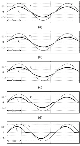
In order to understand the effect of parameter error, several current waveforms are plotted in Fig. 8 where the used nominal values are tabulated in Table IV. Cases (i) and (ii) yield the same value from (19) and thus, contribute to the same clamped current waveforms shown in Fig. 8(a). Likewise, cases (iii) and (iv) have the same value from (19) and thus, they contribute to the same hard-commutation current waveforms in Fig. 8(b). Fig. 8(c) and Fig. 8(d) plot the input current waveforms corresponding to the over-compensation
F and under-compensation 5 . 0 − = k 25 . 0 = k 0 > ∆V ∆VF <0 of
conduction voltages, respectively.
Case (vii) is a special case where zero nominal values rˆL=0, Vˆ =F 0 (i.e. k=−1) are used and longer time of clamped current can be found in Fig. 8(e). In fact, SLCSC in Fig. 3 with zero nominal values can be seen as DPC in Fig. 2. However, all the input currents in Fig. 8 can be found stable and SLCSC is able to operate stably.
D. Comments
The sinusoidal input current case is not practical because we can not determine the real values exactly. However, it is better to keep in clamped current than in hard-commutation current. That is, it is preferred to select a larger nominal value of inductance ( ), smaller nominal values of resistance ( L) and nominal conduction voltage ( ) to operate SMR efficiently
with clamped input current during the design of SLCSC. L Lˆ> L r rˆ < F F V Vˆ < C. Transient Response
In order to understand the transient response of the proposed SLCSC, the simulated waveforms of sudden load change without parameter error and with parameter error are plotted in Fig. 9(a) and Fig. 9(b), respectively. To meet the change of load, the input current magnitude increases from about 6A to about 10A by SLCSC.
In Fig. 9(a), we can find that the sinusoidal current is in phase with the input voltage during the transient period. Although the input current in Fig. 9(b) is clamped to zero due to the parameter error, the output voltage is still well regulated.
s v s i (a) s i s v (b) s v s i (c) 0 -10A 100V 5ms s i vs (d) s i s v (e)
Fig. 8. Simulated input currents with various nominal values tabulated in Table IV.
o v s v s i (a) s v s i o v (b)
Fig. 9. Simulated waveforms during load regulation:
(a) =0, =0, 0; (b) L= , = , L r ∆ ∆L ∆VF = ∆r 0.5rL L ∆ −0.5L ∆VF =0.5VF;
IV.
EXPERIMENTAL
RESULTS
In this paper, SLCSC had been digitally implemented in a FPGA-based system using Xilinx XC3S200 where the DPC and SLCSC in [16-17] were implemented in DSP TMS320F240. Due to the measure uncertainty, it is not easy to obtain the real values. In practice, some circuit parameters, such as inductance, resistance and conduction voltages, may have small fluctuation with the instantaneous input current. However, we measure the parameters as exact as we can. All the measured circuit parameters have been listed in Table III and can be regarded as the nearly exact parameters.
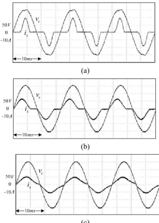
Turning off the single power switch in a boost-type SMR obtains the pulse current waveform plotted in Fig. 10(a) and input current harmonics are tabulated in Table V where the load resistance is decreased to about to yield the rated power 675W. The input current is highly discontinuous and the peak current is high up to 20A.
Ω 30
Fig. 10(b) plots the input current where SLCSC with zero nominal values (i.e. DPC case in Table IV) is used to turn on and turn off the power switch to regulate the output voltage with the rated power 675W. We can find the peak value of the clamped current decreases from 20A to about 12A and the total harmonic distortion factor (THD) decreases to
the half of Fig. 10(a). However, due to the larger phase between the input voltage and input fundamental current in Fig. 10(b) than that in Fig. 10(a), the displacement power factor (DPF) decreases from 0.978 lagging to 0.908 leading.
Fig. 10(c) plots the input current where SLCSC with nearly exact parameters are used to regulate the output voltage. Due to the fluctuation of circuit parameter with temperature and current, the input current is not a pure sinusoidal waveform, but is continuous. Due to the increase of DPF in Fig. 10(c), the peak current decrease to about 10A, and the power factor increases from 0.758 to 0.982 and THD decreases from 76.4% to 12.4%. Because of the continuous current, less current harmonics in Fig. 10(c) is found than those in Fig. 10(b).
s v s i (a) s v s i (b) s v s i (c)
Fig. 10. Experimental input voltages and currents at 675W: (a) for a SMR without turning on the power switch; (b) for a DPC-controlled SMR; (c) for a SLCSC-controlled SMR with nearly exact parameter;.
All the current harmonics are tabulated in Table V where the harmonic limits of IEC-61000-3-2 class A are also listed for comparison. It is noted that the input current waveform in (18) is highly dependent on the parameter errors and the quality factor L in (19) especially when zero nominal values are included in DPC. The PI parameter of voltage loop can improve the response, but do not dominate the compliance of the IEC-61000-3-2 class A. Due to no design optimization in the experiment, the input current harmonics in Fig. 10(c) are compliant
to the limit of class A, but those in Fig. 10(b) are not.
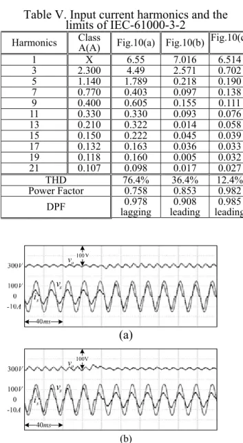
To verify the dynamic performance of the proposed SLCSC with nearly exact parameters, some waveforms are plotted in Fig. 11 where the load condition is suddenly changed between 450W and 675W. During the regulation, the input current keeps in phase with the input voltage. It clearly shows that the proposed SLCSC also possesses good performance of regulation.
Table V. Input current harmonics and the limits of IEC-61000-3-2
Harmonics Class A(A) Fig.10(a) Fig.10(b) Fig.10(c)
1 X 6.55 7.016 6.514 3 2.300 4.49 2.571 0.702 5 1.140 1.789 0.218 0.190 7 0.770 0.403 0.097 0.138 9 0.400 0.605 0.155 0.111 11 0.330 0.330 0.093 0.076 13 0.210 0.322 0.014 0.058 15 0.150 0.222 0.045 0.039 17 0.132 0.163 0.036 0.033 19 0.118 0.160 0.005 0.032 21 0.107 0.098 0.017 0.027 THD 76.4% 36.4% 12.4% Power Factor 0.758 0.853 0.982
DPF lagging 0.978 leading0.908 leading0.985
s v s i o v (a) 0 -10A 100V 300V 40ms s v s i o v100V (b)
Fig. 11. Experimental waveforms when the load is suddenly changed (a) from 450W to 675W; and (b)
from 675W to 450W.
REFERENCES
[1] O. Garcia, J. A. Cobos, R. Prieto, P. Alou, and J. Uceda, “Single phase Power Factor Correction: A Survey,” IEEE
Trans. on Power Electronics, vol. 18, no. 3, pp. 749-754, May
2003.
[2] J. C. Crebier, B. Revol, and J. P. Ferrieux, “Boost-Chopper-Derived PFC Rectifiers: Interest and Reality,”
IEEE Trans. on Industrial Electronics, vol. 52, no. 1, pp. 36-45,
Feb. 2005.
[3] H. C. Chen, S. H. Li, and C. M. Liaw, “Switch-Mode Rectifier with Digital Robust Ripple Compensation and Current Waveform Controls”, IEEE Trans. on Power Electronics, vol. 19, no. 2, pp. 560-566, March 2004.
[4] E. Fiqueres, J. M. Benavent, G. Garcera and M. Pascual, ‘Robust Control of Power-Factor-Correction Rectifiers with Fast Dynamic Response,’ IEEE Trans. on Industrial
Electronics, vol. 52, no. 1, pp. 66-76, Feb. 2005.
[5] J. Zhou, Z. Lu, Z. Lin, Y. Ren, Z. Qian, and Y. Wang, ‘Novel Sampling Algorithm for DSP Controlled 2kW PFC Converter,’
IEEE Trans. on Power Electronics, vol. 16, no. 2, pp. 217-222,
Mar. 2001.
[6] D. M. Van de Sype, K. De Gusseme, A. P. Van den Bossche, and J. A. Melkbeek, ‘A smapling algorithm for digitally controlled boost PFC Converters,’ IEEE Trans. on Power
Electronics, vol. 19, no. 3, pp. 649-657, May. 2004.
[7] D. M. Van, K. D. Gusseme, A. P. M. V and J. A. Melkebeek, “Duty-Ratio Feedforward for Digitally Controlled Boost PFC Converters”, IEEE Trans. on Industrial Electronics, vol. 52, no. 1, pp. 108-115, Jan. 2005.
[8] M. Chen, and J. Sun, “Feedforward Current Control of Boost Single-Phase PFC Converters,” IEEE Trans. on Power
Electronics, vol. 21, no. 2, pp. 338-345, March 2006.
[9] S. C. Yip, D. Y. Qiu, H. S. Chung, and S. Y. R. Hui, “A Novel Voltage Sensorless Control Technique for a Bidirectional AC/DC Converter”, IEEE Trans. on Power Electronics, vol. 18, no. 6, pp. 1346-1355, Nov. 2003.
[10] S. Sivakumar, K. Natarajan, and R. Gudelewicz, “Control of Power Factor Correcting Boost Converter Without Instantaneous Measurement of Input Current,” IEEE Trans. on
Power Electronics, vol. 10, no. 4, pp. 435-445, Jul. 1995.
[11] B. Choi, S. S. Hong and H. Park, “Modeling and Small-Signal Analysis of Controlled On-Time Boost Power-Factor-Correction Circuit,” IEEE Trans. on Industrial
Electronics, vol. 48, no. 1, pp. 136-142, Feb. 2001.
[12] D. Maksimovic, Y. Jang, and R. W. Erickson, “Nonlinear-Carrier Control for High-Power-Factor Boost Rectifiers”, IEEE Trans. on Power Electronics, vol. 11, no. 4, pp. 578-584, Jul. 1996.
[13] J. Rajagopalan, F. C. Lee, and P. Nora, “A General Technique for Derivation of Average Current Mode Control Laws for Single-Phase Power-Factor-Correction Circuits Without Input Voltage Sensing”, IEEE Trans. on Power Electronics, vol. 14, no. 4, pp. 663-672, Jul. 1999.
[14] T. Ohnishi and M. Hojo, “DC Voltage Sensorless Single-Phase PFC Converter,” IEEE Trans. on Power Electronics, vol. 19, no. 2, pp. 404-410, March 2004.
[15] Y. K. Lo, H. J. Chiu and S. Y. Ou, “Constant-Switching-Frequency Control of Switch-Mode Rectifiers Without Current Sensors,” IEEE Trans. on Industrial
Electronics, vol. 47, no. 5, pp. 1172-1174, Oct. 2000.
[16] H. C. Chen, “Duty Phase Control for Single-Phase Boost-Type SMR,” IEEE Trans. on Power Electronics, vol. 23, no. 4, pp. 1927-1934, July 2008.
[17] H. C. Chen, “Single-Loop Current Sensorless Control for Single-Phase Boost-Type SMR,” IEEE Trans. on Power
Electronics, vol. 24, no. 1, pp. 163-171, Jan. 2009.
計畫成果自評
本兩年期計畫第一年計畫,主要分析昇 壓型切換式整流器之電路特性,並以此為 基礎,於第二年進行電壓迴路設計。就目 前成果而言,與當初計畫規劃相符。
![TraditionalMLCalgorithmsmainlytacklethebatchMLCproblem,wheretheinputdataarepresentedinabatch[24,28].Nevertheless,inmanyMLCapplicationssuchase-mailcategorization[22],multi-labelexamplesarriveasastream.Onlineanalysisistherefore dimensionreducermotivatedbyma](data:image/gif;base64,R0lGODlhAQABAIAAAP///wAAACH5BAEAAAAALAAAAAABAAEAAAICRAEAOw==)