國 立 交 通 大 學
電信工程學系
碩 士 論 文
應用於音頻之三角積分調變器之設計與製作
The design and implementation of Sigma-Delta
modulator for audio band applications
研究生:吳俊誼
指導教授:闕河鳴 博士
The design and implementation of Sigma-Delta
modulator for audio band applications
研 究 生:吳俊誼 Student: Jin-Yi Wu
指導教授:闕河鳴 博士 Advisor: Dr. Herming Chiueh
國 立 交 通 大 學
電 信 工 程 學 系 碩 士 班
碩 士 論 文
A Thesis
Submitted to Department of Communication Engineering College of Electrical and Computer Engineering
National Chiao Tung University in Partial Fulfillment of the Requirements
for the Degree of Master of Science in Communication Engineering June 2009 Hsinchu, Taiwan 中 華 民 國 九 十 八 年 六 月
I
應用於音頻之三角積分調變器之設計與製作
研究生:吳俊誼 指導教授:闕河鳴 博士 國立交通大學 電信工程學系碩士班摘要
類比數位轉換器(ADC)一直被大量應用於電子產品,隨著應用的不同,ADC 的選擇及設計非常重要。目前的 ADC 可分為 Flash ADC、Pipeline ADC 和 Sigma-Delta ADC 等,其中 Sigma-Delta ADC 適合應用在低頻寬且需要高解析度 的電子產品,而 Sigma-Delta ADC 未來發展還是朝向高解析度、低功率消耗及低 晶片製作成本的方向以提升效能。其中,信號頻帶在音頻的可攜式裝置,如 mp3 播放器及助聽器所用的 ADC,設計時多會考慮如何增加電池壽命,也就是降低功 率消耗,及降低晶片面積,以方便攜帶且減少成本。 由於可攜式行動裝置的快速成長,電路操作在低電壓低功率已經是一種趨 勢。我們在低功率的前提下,設計一個頻寬在音頻內,擁有高解析度、穩定度且 製作成本低的 Sigma-Delta ADC,應用於中輕度聽障者使用的助聽器,晶片面積 0.058mm2 ,功率消耗 53uW。II
The design and implementation of Sigma-Delta
modulator for audio band applications
Student: Jin-Yi Wu Advisor: Dr. Herming Chiueh SoC Design Lab, Department of Communication Engineering,
College of Electrical and Computer Engineering, National Chiao Tung University Hsinchu 30010, Taiwan
Abstract
Analog-to-digital converters (ADCs) are employed in many electronic products, and it’s important to make a choice between accuracy and speed for different applications. In several kinds of ADCs (Ex: Flash ADC 、 Pipeline ADC and Sigma-Delta ADC), Sigma-Delta ADC is suitable for low speed and high resolution electronic products. The principles when designing Sigma-Delta ADC are high resolution 、low power consumption and low cost. The ADCs which are application for portable devices such as mp3 players and hearing aids would be designed for low power consumption and small chip area.
Because of fast growing of portable devices, circuit operation with low-voltage and low-power is desirable. In the premise of low power consumption, we designed a Sigma-Delta ADC which is high resolution 、high stability and low cost. The ADC is employed in the hearing aids for moderately hearing-impaired. The chip area is 0.058mm2 and power consumption is 53uW.
III
Acknowledgements
本篇碩士論文得以順利完成,首先要感謝的是我的指導教授闕河鳴博士。闕 老師在學生遇到問題時總會循循善誘我們藉由正確的態度得到問題的答案,建立 了我們身為一位碩士所需的思考能力及分析問題的方法,相信這對於我們以後在 職場及人生都有莫大的幫助,我想這是老師希望我們在碩士期間除了專業知識學 習到最重要的東西。 另外,謝謝信太、江俊、嘉儀三位同學在課業及日常生活上的鼎力相助;還 要謝謝秉勳、凱迪、明君、春慧、品翰、是瑜、鎮宇、國哲、鼎國、燦傑、登政 等學弟妹給予的支持及幫忙;還有特別謝謝大學同學主恩及他的父母親楊爸爸、 楊媽媽那樣的照顧我,謝謝所有幫助過我的人,謝謝你們! 最後,謝謝我的父母以及家人,謝謝母親一路上的支持及鼓勵我,讓我能完 成我的學業。 我衷心感謝上述曾提攜或幫助過我的你們,謝謝大家並祝福大家。 吳俊誼 July,17,2009
IV
Content
中文摘要
………..…….. I
English Abstract……….. II
Acknowledgement……….
III
Content………....
IV
List of Tables………..
VI
List of Figures………VII
Chapter 1 Introduction……… 1
1.1 Motivation………..……… 1 1.2 Organization………..…….… 3Chapter 2 Fundamentals of SDM………..……… 4
2.1 A brief Introduction of ADC……….…4
2.2 Oversampling and Noise Shaping……….………….. 7
2.2.1 Oversampling………...………..………...8
2.2.2 Noise Shaping………...………8
2.3 Performance Metrics……….…………. 10
Chapter3 System Level Considerations……….….. 12
3.1 Area Issues in SDM………12
3.2 Supply Voltage Issue in SDM ………13
3.3 System Parameters Considerations………...……….14
3.3.1 Design Target of SDM………14 3.3.2 Topology Decision………15 3.3.3 Architecture Selection………... ….17 3.3.4 Coefficient Decision………..19 3.4 Non-idealities Considerations………...……….20 3.4.1 Gain Requirement………20 3.4.2 Capacitor sizing………..………..……21
V
Chapter 4 Circuit Implementation of SDM…..………..25
4.1 Circuit Level Design………..25
4.2 Transistor Level Design………..27
4.2.1 Differential OP………...………..27
4.2.2 1-bit quantizer………..32
4.2.3 Clock Generator………..33
4.2.4 Switches………..35
4.3 Modulator Design and Simulation………..35
4.4 Layout Level Design………...37
Chapter 5 Testing Setup and Experimental Result
s
……….………….43
5.1 Testing Environment Setup……….43
5.2 Problem of chips……….45 5.3 Performance evaluations………47 5.4 Comparison……….50 5.5 Summary………51
Chapter 6 Conclusions ……….…….………..52
References………53
VI
List of Tables
Table 2.1 Several kinds of ADCs...5
Table 3.1 Comparison of previous researches fabricated in 0.18um technology...…..13
Table 3.2 power consumption of OP in 4 kinds of loop filter order………...16
Table 3.3 SFDR with different parameters after rounding………...19
Table 4.1 Organization of SDM……….…..25
Table 4.2 Device ratio summary of first OP...27
Table4.3 Summary of first OP simulation results………...……….28
Table 4.4 Performance comparison of the two OP………...…28
Table 4.5 CMFB circuit summary………...………….30
Table 4.6 Quantizer transistor size summary………...………32
Table 4.7 Pin Assignments of whole chip……….…...38
Table 4.8 Corner of post-layout simulation...……….…………..40
Table 4.9 Summary of the proposed SDM………...41
Table 4.10 The comparison of this work and previous researches………...42
VII
List of Figures
Figure 2.1 Block diagram of an ADC………4
Figure 2.2 Transfer curve of quantizer………6
Figure 2.3 Figure 2.3 Probability of quantization noise ………6
Figure 2.4 Quantization noise in an oversampled converter……….….………..8
Figure 2.5 A linear model of the sigma-delta modulator………..………9
Figure 2.6 Performance metrics………...11
Figure 3.1.Switch-driving problem in low supply voltage………….………....13
Figure 3.2 Chain of Integrators with distributed feedback (CIFB)………..17
Figure 3.3 Chain of integrators with weighted feed-forward summation (CIFF)….18 Figure 3.4 Parameters of second order CIFB Sigma-Delta modulator topology……19
Figure 3.5 Switched-capacitance circuit in SDM…...………….……….21
Figure 3.6 SFDR versus Cs1 with parameters after rounding …….………..………..23
Figure 3.7 Sampling and integration period of a loop filter………...………..24
Figure 4.1 Circuit level of SDM………...………..…..26
Figure 4.2 Fully differential OPAMP………...………...27
Figure 4.3 Frequency Response of first OP……….…………30
Figure 4.4 Dynamic CMFB circuit………...………31
Figure 4.5 Transient Response of first OP output………31
Figure 4.6 a power-efficient 1-bit quantizer……….32
Figure 4.7 Simulation results of the 1-bit quantizer……….…33
Figure 4.8 Clock generator circuit…..………..34
Figure 4.9 Output of the clock generator……….34
Figure 4.10 2nd order CIFB SDM……….………..36
Figure 4.11 input signal and output signals of two integrators…………..…………..36
Figure 4.12 8192-point output FFT of the pre-simulation result……….37
Figure 4.13 Diagram of the layout……….………..38
Figure 4.14 Diagram of the18 pin DIP package………..38
Figure 4.15a 8192-point FFT of the post-simulation result………...……..40
Figure 4.15b 8192-point FFT of the post-simulation result………...……..40
Figure 4.16 Dynamic range of the SDM…...………….………41
Figure 5.1 experimental test chip…...………44
Figure 5.2 Photograph of the measurement environment…….………...45
Figure 5.3 The problem of clock generator………...………...46
Figure 5.4 The die photo before modifying………...…...…….46
VIII
Figure 5.6 Measured output waveforms of the SDM………...……...…….48
Figure 5.7 Measured output spectrum of the SDM………...……...…….48
Figure 5.8 linear scale PSD……….….49
1
Chapter 1
Introduction
1.1 Motivation
The modern CMOS process has great improvement in the dimension scale down such that the complexity of designing circuit is becoming higher. For example, the threshold of device is not scaled down in proportion to supply voltage. Thus it increases the difficulty of circuit design.
Power consumption is always an issue for portable devices such as cell phones, mp3 players, hearing aid instruments, and hand-held videogames. The low power consumption increases the battery-life. The power consumption is in proportion to square of supply voltage. Low voltage circuit design is an efficiency way to save power consumption.
Another issue for portable devices is area. Small area makes the devices more and more exquisite, and it decrease the cost for business concern. Thus smaller area is another point in my design.
Analog-to-digital converters (ADCs) are employed in many electronic products, and it’s important to make a choice between accuracy and speed for different applications. In several kinds of ADCs (Ex: Flash ADC 、 Pipeline ADC and Sigma-Delta ADC), Sigma-Delta ADC is suitable for low speed and high resolution
2
electronic products. By over-sampling and noise shaping, the sigma-delta ADCs transfer most of the signal processing tasks to the digital domain. And it only requires relaxed anti-aliasing filter. Therefore, for high-resolution ADCs, the sigma-delta ADCs are power and area effiency compared to other architectures.
Therefore, the design target of this design is to achieve a low-power and small-area audio band sigma-delta ADC. The SDM is application to hearing aids for moderately hearing-impaired. It have been fabricated in a standard 0.18um CMOS technology, and provide a SNDR of 58dB with measurement for audio band signal bandwidth (8k) and it dissipates 53uW, the core area is 0.058mm2, and it will compare with other SDM by figure of merit (FOM).
3
1.2 Organization
In Chapter 2, the beginning is the overview of the analog-to-digital converters (ADC). After them, the quantization issues, oversampling and noise shaping are introduced. Then the performance metrics of sigma-delta modulators (SDM) end this chapter.
Chapter 3 describes the system level design considerations, including power supply and area issues of SDM, the topology and the important parameters selections of the SDM.
Chapter 4 discusses the topics of sub-circuits that will be used to realize an actual integrated circuit, which covers an operational amplifier (OPAMP), a comparator, switches and capacitors. The simulation results and device ratios are given at each section. The circuit level, transistor level, and layout level design will be described in sequence.
In chapter 5, the testing environment is present, including the instruments and external testing circuits on printed circuit board (PCB). Experimental results for a SDM, which is fabricated in a 0.18μm 1P6M1.8V standard CMOS with MIM process, will be plotted and summarized.
4
Chapter 2
Fundamentals of SDM
In this chapter, we begin with a brief overview of analog-digital converter (ADC) in the aspects of speed and architecture. Following by the classification of ADC, the oversampling and noise shaping is introduced and defined mathematically. The performance metrics of targeting ADC is then described in the end of this chapter.
2.1 A brief Introduction of ADC
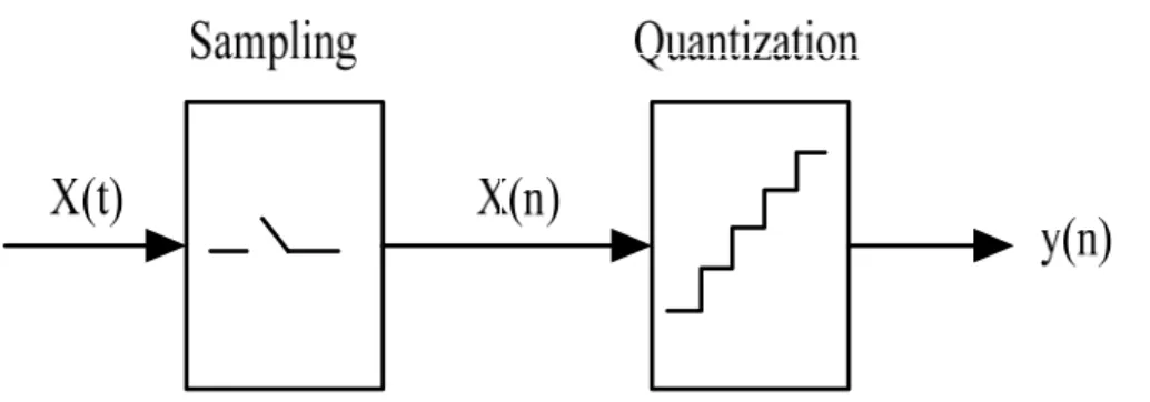
The ADCs are fed a continuous-time analog signal to convert discrete-levels. To convert a continuous-time analog signal into a digital one, two operations should be performed. First, we discretize the continuous analog signal by sampling circuit. After sampling, the quantization is followed by digitizing the amplitude of the discrete signal, as shown in Figure 2.1.
5
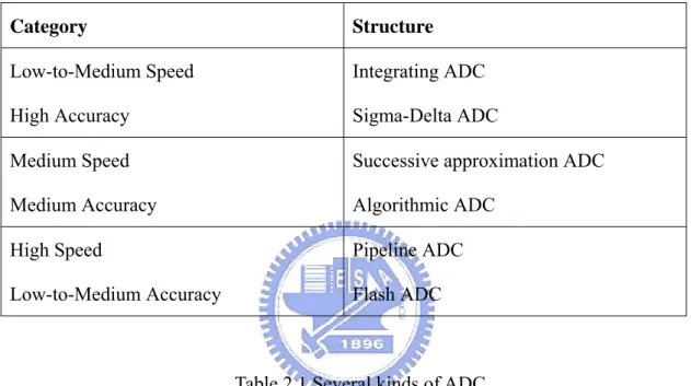
Analog-to-digital converters (ADCs) are employed in many electronic products, and it is important to make a choice between accuracy and speed for different applications. Several types of ADCs are developed for different speed and resolution requirements as depicted in Table 2.1 and Figure 2.2. In the ADCs, sigma-delta ADC is suitable for high resolution application in audio band.
Category Structure Low-to-Medium Speed High Accuracy Integrating ADC Sigma-Delta ADC Medium Speed Medium Accuracy
Successive approximation ADC Algorithmic ADC
High Speed
Low-to-Medium Accuracy
Pipeline ADC Flash ADC
Table 2.1 Several kinds of ADC
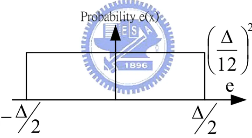
The quantization stepΔ is called the least significant bit (LSB) of the ADC, as shown in Figure 2.2. It is often desirable to approximate when the data pass through the quantizer. The deviation of the real data from the approximate is called quantization error or quantization noise. And quantization error is less than a half of LSB.
If we assume that the quantization noise is white noise, it is uniformly distributed between
2
LSB
± , as shown in Figure 2.3:
6
Figure 2.2 Transfer curve of quantizer
2
12
⎟
⎠
⎞
⎜
⎝
⎛ Δ
2
Δ
−
2
Δ
Figure 2.3 Probability of quantization noiseTherefore, the power of the quantization error can be derived as: 2 2
( )
12
e qP
e
ρ
e de
∞ −∞Δ
=
∫
=
(2.1)7
For a sinusoidal input signal, its maximum peak value without clipping is 2 2
N Δ,
where N is the bit number of the quantizer. Thus the sinusoidal signal power equals to: 2 2 2 1 2 2 2 2 8 N N in P = ⎛⎜ Δ⎞⎟ = Δ ⎝ ⎠ (2.3)
From the equation, if the quantization noise can be modeled as a noise source, we can calculate the signal-noise-ratio (SNR) of an ideal N-bit ADC:
( )
2 2 2 2 2 3 810log 10log 10log 2 10log 6.02 1.76( ) 2 12 N N in peak e P SNR N dB P ⎛Δ ⎞ ⎜ ⎟ ⎛ ⎞ ⎛ ⎞ = ⎜ ⎟= ⎜ Δ ⎟= + ⎜ ⎟⎝ ⎠= + ⎜ ⎟ ⎝ ⎠ ⎜ ⎟ ⎝ ⎠ (2.4)
It can be found that increase one bit resolution of the quantizer gives the SNR improvement of 6.02dB.
2.2 Oversampling and Noise Shaping
This section describes the principle and the theorem of the digital signal processing technique. We discuss oversampling first, which is followed by noise shaping.
8
2.2.1 Oversampling
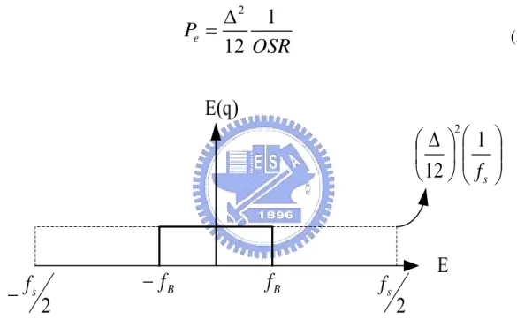
For a signal bandwidth of f , the Nyquist rate is 2B f .A Nyquist ADC represent B
that the sampling frequency of the ADC is at Nyquist rate. Moreover, an ADC with the oversampling technique can also improve the SNR. Its sampling rate f is greater S
more times than the signal bandwidth 2f , and the oversampling ratio is defined B
as B s f f OSR 2
= , as Figure. 2.4, than the quantization power spectral density is reduced to: 2
1
12
eP
OSR
Δ
=
(2.5)2
sf
2
sf
−
−
f
Bf
B⎟⎟
⎠
⎞
⎜⎜
⎝
⎛
⎟
⎠
⎞
⎜
⎝
⎛ Δ
sf
1
12
2Figure 2.4 Quantization noise in an oversampled converter Thus the peak SNR equals to:
(
OSR
)
N
P
P
SNR
e inpeak
10
log
⎟⎟
=
6
.
02
+
1
.
76
+
10
log
⎠
⎞
⎜⎜
⎝
⎛
=
(2.6)2.2.2 Noise Shaping
With oversampling technique, the SNR increase 0.5 bit if sampling frequency is doubling. In addition to use oversampling technique to improve the performance of
9
ADCs, we can use noise shaping technique to further increase the SNR of the ADC, by applying a loop filter before the quantizer and introducing the feedback, a
noise-shaping modulator is built and new noise transfer function is realized.
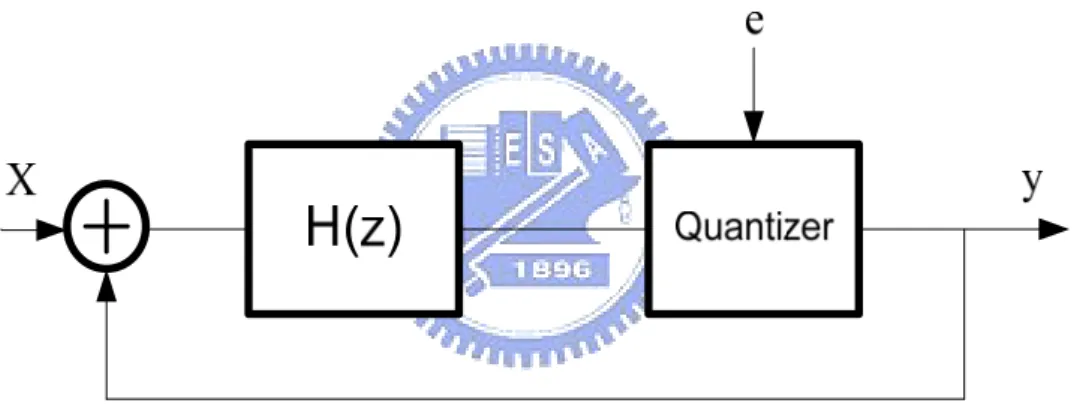
A basic Sigma-Delta modulator is shown in Figure 2.5, it contains a loop filter, a quantizer and a feedback loop. If we assume that the DAC feedback gain is unity, than we can express the output of the SDM is:
( )
( ) ( )
( ) ( )
Y z
=
STF z X z
+
NTF z E z
(2.7)Figure 2.5 A linear model of the sigma-delta modulator
Where STF(z) represents the signal transfer function and NTF(z) represents the noise transfer function. And the STF(z) and NTF(z) can be calculated as:
( )
( )
( )
( ) 1
( )
Y z
H z
STF z
X z
H z
=
=
+
(2.8)( )
1
( )
( ) 1
( )
Y z
NTF z
E z
H z
=
=
+
(2.9)10
With the large gain of H(z) at the frequency band, the STF(z) will approximate unity and the NTF(z) is going to approximate zero over the signal band. Thus the quantization noise is further attenuated than only by oversampling.
2.3 Performance Metrics
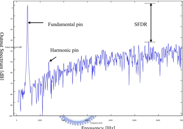
The performance metrics is shown at Figure 2.6 with a full scale sine wave to ADC, performed a Discrete Fourier Transform (DFT) to map into Fast Fourier Transform (FFT) spectrum. Some of the performance metrics are listed below, while the unit is “dB”.
1. SFDR: the abbreviation of “spurious free dynamic range”. Difference between the fundamental bin and the highest harmonic bin.
2. SNR: the abbreviation of “signal to noise ratio”. Fundamental power divided by the power of the bins in the FFT other than DC, fundamental and first N harmonic bins.
3. SNDR: the abbreviation of “signal to noise and distortion ratio”. Fundamental power divided by the power of the bins in the FFT other than DC and fundamental bins.
4. ENOB: the abbreviation of “effective number of bits”, which is defined at Equation 2.10:
11
5. DR: the abbreviation of “dynamic range”. Effective input range when SNR remains positive.
Figure 2.6 Performance metrics
0 1000 2000 3000 4000 5000 6000 7000 -100 -90 -80 -70 -60 -50 -40 -30 -20 -10 0 Frequency [Hz] Output spectrum [dB] Fundamental pin Harmonic pin SFDR Frequency [Hz] Output Spectrum [dB]
12
Chapter 3
System Level Design Considerations
This chapter discusses actual SDM design considerations. First, we review previous researches fabricated in 0.18um technology for audio band applications. Some researches consider power issue and one of them focus on area. And then the system parameter considerations are discussed in Section 3.2. Several non-idealities such as gain requirement, settling of opamp and capacitor sizing are discussed in the end of the chapter.
3.1 Area Issues in SDM
In order to realize an area-efficient switched-capacitor circuit, capacitors with high capacitance per unit area are required. An opportunity to achieve the condition is using MOSFET capacitances (MOSACAPs). But MOSACAPs should only be used when high linearity is not required [4]. So we decide to adopt metal-insulator-metal capacitors (MIMCAPs) for the switched-capacitor circuit. And we optimize the capacitor value used in the circuit by simulation to reduce the area. The area of my design is proven to be as large as the SDM of Ref [4] after layout. The process will be shown later.
13 Signal bandwidth (Hz) Clock frequency (Hz) OSR SNDR (dB) Area mm2 Supply voltage (V) Power (uW) [4] (JSSC 2002) 8k 1M 64 67 0.082 0.7 80 [5] (ISCAS 2003) 10k 2M 100 71 0.27 0.9 37.7 [6] (CICC 2001) 16k 1M 32 66.5 0.17 1 140 [7] (ISCAS 2003) 8k 1M 64 69.2 0.096 0.65 130
Table 3.1 Comparison of previous researches fabricated in 0.18um technology
3.2 Supply Voltage Issue in SDM
Supply voltage in modern CMOS process is continuously decreasing .Thus the switch-driving problem is brought for switched capacitor (SC) circuits at low supply voltage. When Supply voltage (VDD) is lower than the sum of the threshold voltage of n-and p-MOSFETs (Vtn+Vtp), the circuit may not work correctly as shown in Fig.3.1.
Vin
both on
both off
Small headroom No headroom
Vin Vout
Problem of CMOS s witch
Vtn Vtn Vtp Vtp PMOS on PMOS on NMOS on NMOS on VDD VDD VDD VDD
14
A switched-OPamp technique combined with a dc level shift has been proven to allow proper operation under low VDD conditions (1v,0.7v,0.65v), thus lower the power consumption[4][6][7]; A new fully differential CMOS class AB Operational Amplifier with a charge-pump is proposed to avoid the switch-driving problem [5].Thus it will increase the complexity when designing circuit at low supply voltage. So we make the supply voltage a bit higher than Vtn+Vtp to reduce the complexity when designing circuit. Finally, we will show that the overall power consumption of the SDM is acceptable.
3.3 System Parameter Considerations
The design goal is to design a low power consumption and small-area SDM while the target SNR (DR) is high enough for hearing-aid applications. There are many trade-offs when designing a low-power and small-area SDM, thus three steps are followed in this section to determine the system parameters of the SDM, topology decision, architecture selection and coefficient decision, respectively.
3.3.1 Design target of SDM
First, we decide the specification of SDM in three aspects: supply voltage, signal- bandwidth and resolution.
1. We design a Sigma-Delta modulator in hearing aid operating at 1V supply voltage with zinc air battery (open circuit voltage 1~1.2V).
2. Although normal-hearing humans can detect approximately from about 20Hz to about 20kHz, hearing aids have been limited to a spectral response of 6kHz. [8] [9]
15
Speech articulation range is 200Hz to 6kHz, and considering some consonants in high frequency, we choose the signal bandwidth of Sigma-Delta modulator is 8kHz.
3. 9bit resolution (SNDR =55dB) of Sigma-Delta modulator is enough to compensate 41~55dB hearing loss for moderately hearing-impaired.
3.3.2 Topology Decision
The first step to design a sigma-delta modulator is to determine the system level parameters based on the modulator specifications to lower the power consumption. The power consumption formula:
Power
= × = × ×
I V
f
c
(
Vdd
)
2 (3.1) Therefore, we must choose the supply voltage we used in this thesis. The basic principle is to reduce power, and in TSMC 0.18um technology, vtn+vtp is about 0.9v, so we choose supply voltage is 1v for our design.The system-level parameters include oversampling ratio (OSR), the loop filter order (L), the number of the quantizer level (N).
First we decide N. Because the power consumption of the quantizer increases proportionally with N, and a multi-bit quantizer have more complicated DAC structure, thus will make whole circuit more complicated and consume more power, so for a low-power SDM design, the number of the quantizer should be minimized, so we choose N=1.
16
Second, because single-stage structure has more advantages on low-power design, for example simple analog circuit, good circuit mismatch characteristic, so single stage architecture is selected.
Therefore, for a target SNR, the oversampling ratio (OSR) can be made after deciding the loop filter order n:
(
)
2 13
10 log
2
1
2
n in peak eP
OSR
SNR
n
P
π
π
+⎛
⎞
⎛
⎞
=
⎜
⎟
=
+
⎜
⎟
⎝
⎠
⎝
⎠
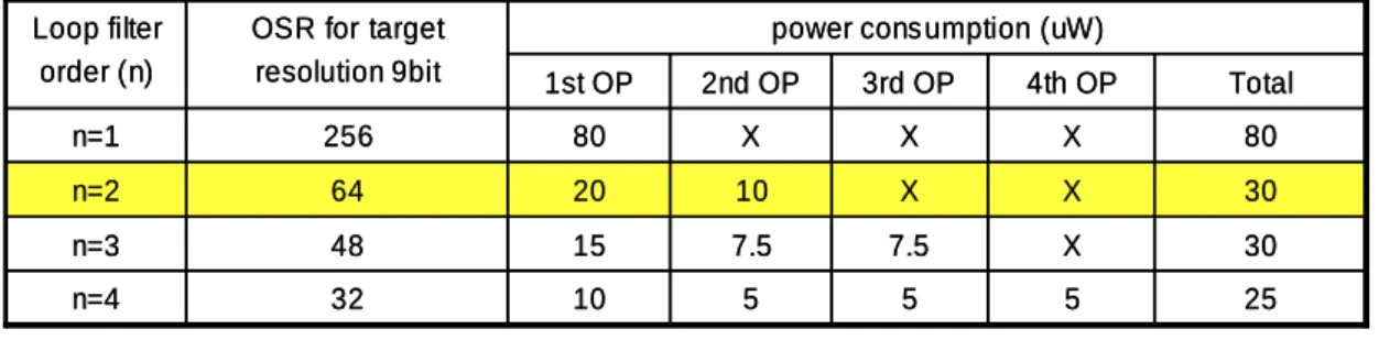
(3.2)A higher loop filler order n have more switches and integrators, lower sampling frequency and higher order of n has more stability issue. So we have to make a trade-off between the order and the sampling frequency. If we compare different order N by simple estimation (We suppose the power consumption of OP is proportional to unity-gain frequency), we can know that for loop filter order 2and 3, we can have similar power consumption as Table 3.2 shows.
80 X X X 80 256 n=1
power cons umption (uW)
5 X X 4th OP 25 5 5 10 32 n=4 30 7.5 7.5 15 48 n=3 30 X 10 20 64 n=2 Total 3rd OP 2nd OP 1st OP
OSR for target resolution 9bit Loop filter order (n) 80 X X X 80 256 n=1
power cons umption (uW)
5 X X 4th OP 25 5 5 10 32 n=4 30 7.5 7.5 15 48 n=3 30 X 10 20 64 n=2 Total 3rd OP 2nd OP 1st OP
OSR for target resolution 9bit Loop filter
order (n)
Table 3.2 power consumption of OP in 4 kinds of loop filter order
From the table above, we choose loop filter order n=2, OSR=64 for power and area efficiency to achieve our target SNR.
17
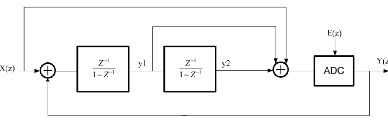
3.3.3 Architecture Selection
The most general single stage topology in the SDM design is the CIFB architecture, and it is shown at Figure 3.2:1 1 1 − − − Z Z 1 1 1 − − − Z Z
Figure 3.2 Chain of Integrators with distributed feedback(CIFB)
The output of integrator one and two are:
( )
(
1
)
(
)
)
1
(
1
1 1 1 1z
E
Z
Z
Z
X
Z
Z
y
=
−−
−−
−−
− (3.3)( )
(
1
)
(
)
2
2 1 1z
E
Z
Z
Z
X
Z
y
=
−−
−−
− (3.4)The outputs depend on the input signal. Thus the disadvantage of CIFB is that it needs large signal swing at the output of the integrators and may consume more power. The advantage is that it is low sensitivity to component variations [14]
Another single stage topology in the SDM design is the CIFF architecture, and it is shown at Figure 3.3:
18 1 1 1 − − − Z Z 1 1 1 − − − Z Z
Figure 3.3 Chain of integrators with weighted feed-forward summation. (CIFF)
The output of integrator one and two are:
( )
Z
E
Z
Z
y
1
=
−
−1(
1
−
−1)
(3.5)( )
Z
E
Z
y
2
=
−
−2 (3.6) The outputs are independent of the input signal. Thus the advantage of CIFF is that it reduces output swing which does not depend on the input signal and may operate with low voltage. The disadvantage is that the out-of-band frequencies due to high frequency boost can overload the quantizer and drive the modulator into instability. [14]Because We have made the supply voltage at 1 volt, the advantage of CIFF is not apparent in my design. Thus we choose the CIFB structure for system stability and we should care the issue of output swing.
19
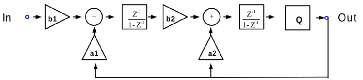
3.3.4 Coefficient Decision
In a general structure of CIFB sigma-delta modulator like Figure 3.4, the modulator contains five coefficients: two integrator gain (b1, b2) and two feedback factor ( a1, a2): 1 --1 Z -1 Z In b1 b2 Out a1 a2 Q 1 --1 Z -1 Z
Figure 3.4 Parameters of second order CIFB Sigma-Delta modulator topology We can use Matlab and the toolbox to get the parameters [3]. The sigma-delta modulator is OSR=64, loop filter order=2, Cascade-of-integrators feedback form (CIFB) structure, we can get:
a1 =0.2636 b1= 0.2636 a2= 0.2249 b2=0.3254
The parameters should be ratio of unit capacitor. Thus we round the parameters to simple ratios when considering layout of capacitors. The unit capacitor is 0.1pf which is the smallest capacitor value in my design. Because of a1 is equal to b1, we simulate 8 times to get the best performance with the parameters after rounding. It is shown in Table.3.3
20 Parameters SFDR (dB) a1 =0.2636 b1= 0.2636 a2= 0.2249 b2=0.3254 73.2 a1 =1/4 b1= 1/4 a2= 1/5 b2=1/4 71.6 a1 =2/7 b1= 2/7 a2= 1/5 b2=1/4 70.7 a1 =1/4 b1= 1/4 a2= 1/4 b2=1/4 69.8 a1 =2/7 b1= 2/7 a2=1/4 b2=1/4 67.4 a1 =1/4 b1= 1/4 a2= 1/5 b2=1/3 72.2 a1 =2/7 b1= 2/7 a2= 1/5 b2=1/3 70.1 a1 =1/4 b1= 1/4 a2= 1/4 b2=1/3 72.6 a1 =2/7 b1=2/7 a2= 1/4 b2=1/3 70.4
Table.3.3 SFDR with different parameters after rounding
Thus we make a1 =1/4 b1= 1/4 a2= 1/4 b2=1/3 to get better SFDR.
3.4 Non-idealities Considerations
There are some non-ideal effects in analog circuit design and it is unavoidable, so we must evaluate the non-ideal effect to make our designs meet the desired margin.
3.4.1 Gain requirement
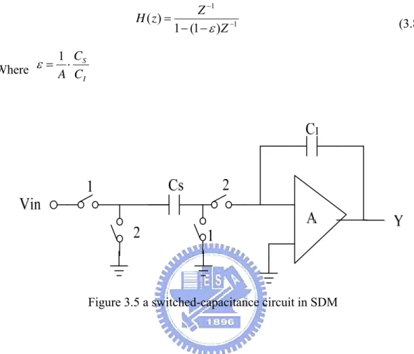
The transfer function of an ideal integrator:
1 1 1 ) ( − − − = Z Z z H (3.7)
21
However, the gain of OP cannot be infinite in circuit design, when a finite gain is A in an OP, the transfer function will become:
1 1 ) 1 ( 1 ) ( − − − − = Z Z z H ε (3.8) Where I S C C A⋅ = 1 ε
Figure 3.5 a switched-capacitance circuit in SDM
A finite gain of OP means that the pole of the H(Z) will depart from unit circle, and when the distance of the zero exceed about
1 1 S I C C OSR⋅ π
, the noise attenuation of NTF begins to degrade, so the lower limit of A is recommended to be 30 dB or more[3]. And after simulation, OP dc gain 50dB is chosen for 2bit resolution margin for the target when per-layout simulation.
3.4.2 Capacitor Sizing
The input-referred thermal noise of the integrator is:
s n
C KT
22
Cs is sampling capacitor of the integrator.
With an oversampling ratio of OSR, the in-band KT/C noise:
(
OSR)
C KT V s n = ⋅ 2 ' (3.10)And if for a full scale input amplitude, the in-band noise power must be at least 78dB below the signal power [3]:
2 1 2 10 2 8 . 7 2 ' ⎟ ⋅ ⎠ ⎞ ⎜ ⎝ ⎛ ⋅ ≤ − DD n V V (3.11) Ö C KTV SNR
(
OSRpeak)
DD S ⋅ ⋅ >8 (2 _ ) [2] (3.12) With OSR=64, VDD=1V, SNR=72dB,we can get Cs is about 8.2fF, but after simulation it only reach SFDR 50dB. Thus we simulate with Cs from 8.2fF to 1pF to get the proper Cs as shown in Figure 3.6.
From Fig.3.5, we find that Cs should be larger than 0.1pf to satisfy the goal. We set the Cs = 0.2pF => SFDR =72.6dB, SNDR=67.7dB
23
Figure 3.6 SFDR versus Cs1 with parameters after rounding
The KT/C noise at the input of the second integrator is shaped by the first-order noise shaping, so that Cs2 can be scaled down since its effect of thermal noise is fewer. In this SDM system, we choose CS2=0.1pF.
3.4.3 Slew rate of the OP
In a switched-capacitance circuit, the loop filter can be separately into two parts, namely the sampling period and the integration period, as shown at Figure 3.7:
To estimate the slew current, the largest quantity of charge may need to be transferred from the sampling capacitor Cs to the integrating capacitors is CsVDD.
We allocate 25% of a half clock period for slewing [3] Cs1(pF) SFDR (dB) 0 0.05 0.1 0.15 0.2 0.25 0.3 0.35 0.4 0.45 0.5 50 55 60 65 70 75
0.2pf
24
the slew current is :
The slew rate is about 2.7V/us when simulation.
Figure 3.7 Sampling and integration period of a loop filter
uA fCsVdd
25
Chapter 4
Circuit Implementation of SDM
The proposed sigma-delta modulator has been fabricated in TSMC 0.18um CMOS standard process. The circuitry is operating at a supply voltage of 1 volt. The
sub-circuitry of each component which includes OP, comparator, clock generator and switched capacitor circuit is described in Section 4.1. In Section 4.2, the simulation results of sub-blocks and whole SDM are presented. In Section 4.3, the final layout design of proposed SDM is then described.
4.1 Circuit Level Design
The detail schematic design and system considerations have been present in earlier this thesis. Implementation of these principles to an actually monolithic chip is our objective here. Let us recall all of building blocks of SDM, they are a loop filter, a quantizer, switches and capacitors. We should notice that a loop filter can be carried out by a differential SC integrator, and the sample and hold circuit can be omitted. In addition to this, a one-bit ADC is used be to be a quantizer for SDM. Therefore the SDM can be divided into two parts, which consist of sub-circuits, and we can summarize them in Table 4.1 below.
A fully experimental SDM circuit is shown in Figure 4.1 at next page, input signal Vi and output signal q are illustrated.
26
Schematic Building
block
Sub-circuit
Section
OPAMP 4.2.1
Loop
filter
Differential
SC Integrator
Switches & capacitors4.2.2
Quantizer 1-bit
ADC Comparator 4.2.3
Table 4.1 Organization of SDM + -+ + -+ Cs1a Cs1b Cs2a Cs2b gnd gnd gnd gnd vdd vdd vdd vdd vi1 vi2 q qb vcmi vcmi vcmi vcmi vcmo vcmo vcmo vcmo Ci1a Ci1b Ci2a Ci2b Cfb2a Cfb2a q qb qb q qb qb q q vcmi vcmi
OPAMP1
OPAMP2
Com parator
27
4.2 Transistor Level Design
This section described the elaboration of sub-circuits that will be used to realize an actual integrated circuit, which covers an operational amplifier (OPAMP), a comparator, switches and capacitors. The simulation results and device ratios are given at each section.
4.2.1 Differential OPAMP
Utilizing switched-capacitor technology and an operational amplifier (OPAMP) to realize a loop filter in a SDM is a common circuitry for low speed and high accuracy applications. It is clearly that, however, the performance of this loop filter dominates dynamic specifications of a SDM. Designing a low power OPAMP to satisfy our goal is the main purpose in this section. The OPAMP is shown at Figure 4.2. In addition to a main circuit, a bias circuit and a common mode feedback circuit (CMFB) will be discussed. VDD Vi1 Vi2 Vb1 Vb3 Vb2 Vo1 Vo2 V1 CMFB 1st stage 2nd stage Av1= gm1[ro6+gm6ro6(ro2〃ro4)] Av2= gm14(ro14〃ro12)
M1 M2 M3 M4 M5 M6 M7 M8 M9 M10 M11 M12 M13 M14 M15
Ref : [4]
(JSSC 2002) C1 C2 Mc2 Mc128
The OPAMP circuit consists of eleven transistors, from M1 to M15. The first stage consists of a PMOS input pair M1, M2 and a folded load consisting of four equal sized PMOS transistors M8-M11. A differential signal sees a high load impedance since the gm’s of the transistors M10 and M11 are cancelled by the gm’s of the cross coupled devices.The second stage is output stage which consists of the common source connected gain transistors M14 and M15 and the current source loads M12 and M13. Mc1 and Mc2 are used as resistors with the compensating capacitor C1, C2 to compensate the phase margin. The transistor size summary of the first OP is shown at Table 4.2: Transistor W L M M1,M2 0.4 0.4 4 M3 0.4 0.4 8 M4,M5 0.8 0.4 2 M6,M7 0.4 0.4 2 M8,M9,M10,M11 1 0.4 2 M12,M13 2 0.4 1 M14,M15 1.6 0.4 4 Mc1,Mc2 0.4 0.4 2
Table 4.2 Device ratio summary of first OP The decision of the size is based on the following principles: (1) The current density is matched.
(2) Tune M1, M2 to meet the gm and Fu specification. (3) Tune M3 to supply the current for M1, M2.
(4) Tune M8~M11 to make a high load impedance for differential signal.
(5) Tune M12~M5 that the output stage has a output closed to 0.5VDD, and the gain of the whole OP exceed 50dB.
29
The performance summary of the first OP is listed at Table 4.3:
Specification Result
DC gain 50.8dB
Phase margin 71.4°
Slew rate 2.68V/us
ICMR (input common mode range) 960mv
Output Swing -950mv~950mv
PSRR 97dB CMRR 68dB
GB 7.1MHz Power 20.2uW
Table 4.3 Summary of first OP simulation results
The comparison of the two OP for a 1.6pf loading capacitance is listed at Table 4.4, and the frequency response of the first OP is shown at Figure 4.7:
Gain(dB) GBW Total Power
OP1 50.8dB 7.1MHz 20.2uW
OP2 50.6dB 5MHz 8.8uW Table 4.4 Performance comparison of the two OP
30
Figure 4.3 Frequency Response of first OP
Because of the differential architecture of the OP, we must have a CMFB circuit which is used because it is the most power-efficient. as shown at Figure 4.4. In the CMFB circuit, Vcmo is set to 0.5v and only the switch connect to CMFB use CMOS switch, other switches is PMOS switch only.
C1a C1b C2a C2b CM Vo1 Vo2 Vcmo Vcmo Vcmo Vcmo
31
Figure 4.4 Dynamic CMFB circuit
The device ratio summary we used in CMFB circuit is listed at Table 4.4, and the transient response of the first OP and CMFB circuit is shown below at Figure 4.9:
Transistor Type W/L Transistor Type W/L
PMOS 2/0.4 NMOS 1/0.4 Capacitor Value Capacitor Value
C1 0.2pf C2 0.4pf Table 4.5 CMFB circuit summary
Figure 4.5 Transient Response of first OP output
4.2.2 1-bit Quantizer
The 1-bit quantizer is realized with a comparator and a SR latch, shown at Figure 4.6. The comparator is a dynamic comparator which has lower average power consumption, when CLK1 is high, the comparator compares the two input voltage, and the comparison result is followed by the SR latch behind the comparator.
32 inp inn CLK1 outn outp Comparator SR latch M1a M1b M2a M2b M3a M3b M4a M4b M5a M5b M6a M6b M7a M7b M8a M8b M9a M9b Figure 4.6 a power-efficient 1-bit quantizer
The simulation result of the 1-bit quantizer is shown at Figure 4.7, for a 10KHz input signal and a clock of 1MHz, the quantizer compare the input signal correctly. After the simulation result, the device ratio of the quantizer is listed at Table 4.6.
33 Width(um) Length(um) M M1a,b 4 0.4 1 M2a,b~M5a,b 1 0.4 1 M6a,b 1 0.4 5 M7a,b 1 0.4 1 M8a,b 1 0.4 5 M9a,b 0.5 0.4 1 Table 4.6 Quantizer transistor size summary
4.2.3 Clock Generator
The on-chip clock generator is shown as Figure 4.8, an external clock input signal is buffered and then two non-overlapping clock phases are generated. To avoid the signal dependent charge injection, two delayed clocks, i.e., C1d and C2d, are also be generated. clk clk1 clk1d clk2 clk2d Figure 4.8 Clock generator circuit
34
The outputs of the clock generator are four different clock phase, the simulation results are shown at Figure 4.9 which shows that the phase one and two are non-overlapped each other.
Figure 4.9 Output of the clock generator
4.2.4 Switches
The current of a MOS switch:
(
GS DS)
DS ox n DV
V
V
L
W
C
u
I
=
−
(4.1) The turn-on resistance of the NMOS, PMOS and CMOS switches can be derived as:)
(
1
in tn DD OX n NMOSV
V
V
L
W
C
u
R
−
−
=
(4.2)35
)
(
1
SS tp in OX n PMOSV
V
V
L
W
C
u
R
−
−
=
(4.3))
(
1
//
)
(
1
SS tp in OX n in tn DD OX n CMOSV
V
V
L
W
C
u
V
V
V
L
W
C
u
R
−
−
−
−
=
(4.4) It is clearly that:(1) A bigger device ratio has smaller turn on resistances, but larger area is resulted. (2) Use NMOS switch as much as we can due to the area consideration.
(3) When the signal of the MOS switch is large, for example, input signal and feedback signal, use CMOS switch.
4.3 Modulator Design and Simulation
A second-order sigma-delta modulator with CIFB topology is done as Figure 4.10:
+ -+ + -+ Cs1a Cs1b Cs2a Cs2b gnd gnd gnd gnd vdd vdd vdd vdd vi1 vi2 q qb vcmi vcmi vcmi vcmi vcmo vcmo vcmo vcmo Ci1a Ci1b Ci2a Ci2b Cfb2a Cfb2a q qb qb q qb qb q q vcmi vcmi
OPAMP1 OPAMP2 Com parator
36
The Sigma-Delta modulator is implemented by fully differential input and output signal, the building blocks in this figure are done as we described in previous sections. With a 4kHz sinusoidal input signal and a -6dB full scale input amplitude, the simulated time-domain integrator output signal and the frequency-domain output spectrum can be observed by Figure 4.11 and Figure 4.12, respectively:
37
Figure 4.12 8192-point output FFT of the pre-simulation result
4.4 Layout Level Design
A physical design in the context of integrated circuit is referred to as layout. Effects of parasitic components and mismatching will damage the performance of the chip, so layouts must be considered heavily in design process. Several principles of layout must be obeyed to minimize cross-talk, mismatches include (a) multi-finger transistors (b) symmetry (c) dummy cell (d) common centroid.
The diagram of layouts are shown at Figure 4.13, there are eighteen I/O pads, including a pair of differential inputs, a pair of modulator outputs, a input clock, three VDD and GND for analog and digital circuit, a pair of clock for measurement, others for reference voltages. The I/O pad description is listed at Table 4.7. This circuit is fabricated in a TSMC 0.18 um CMOS Mixed Signal RF General Purpose Standard Process FSG Al 1P6M process. The chip area is 0.349mm2 including I/O pads and
102 103 104 105 106 -120 -100 -80 -60 -40 -20 0 Frequency [Hz] Output Spectrum [dB]
Input signal =4kHz SFDR=73B SNDR=68dB
38
0.058mm2 for the core area.
Clock 1st stage
2nd stage
comparator
Figure 4.13 Diagram of the layout
The package type of proposed chip is S/B type 18 pin, as shown in Figure 4.14.
39
Pin Name Description
1 CLK Input clock signal
2 CK1d Output clock for measurement
3 CK2 Output clock for measuremen
4 Agrgnd Ground for analog circuit guard ring
5 Vbias Voltage for bias circuit
6 Vcmo Reference voltage
7 Vcmi Reference voltage
8 Vrefn Reference voltage
9 Vrefp Reference voltage
10 Vin1 Differential input signal
11 Vin2 Differential input signal
12 Agnd Ground for analog circuit
13 Avdd VDD for analog circuit
14 Vout1 Differentail output signal
15 Vout2 Differentail output signal
16 Dgrgnd Ground for digital circuit guard ring
17 Dgnd Ground for digital circuit
18 Dvdd VDD for digital circuit
Table 4.7 Pin Assignments of whole chip
The 8192-point FFT of the post simulation result is shown as Figure 4.15 with the input frequency of 4k and1k and the input amplitude is -6dB of full scale.
40
Figure 4.15a 8192-point FFT of the post-simulation result
Figure 4.15b 8192-point FFT of the post-simulation result
102 103 104 105 106 -100 -90 -80 -70 -60 -50 -40 -30 -20 -10 0
Input signal =1kHz SFDR=69dB SNDR=63dB
Frequency [Hz] Output Spectrum [dB] 102 103 104 105 106 -120 -100 -80 -60 -40 -20 0 Output Spectrum [dB] Frequency [Hz]Input signal =4kHz SFDR=72dB SNDR=66dB
41
Because of the possibly process variation, we simulate the SNR results for corners, the corner simulation results are summarized at Table 4.8.
TT FF SS
SFDR (dB) 72 69 69
SNDR (dB) 66 64 63
Table 4.8 Corner of post-layout simualtion
The dynamic range is 74dB as Figure 4.16 shows.
-80 -70 -60 -50 -40 -30 -20 -10 0 0 10 20 30 40 50 60 70 80
Figure 4.16 Dynamic range of the SDM Vin/Vref (dB)
42
Finally, the performance summary of the proposed SDM is listed at Table 4.9, the simulation result shows that the peak SNDR is 66dB for a 4 KHz signal bandwidth and sampling frequency of 1MHz. The difference in SNDR between Pre-Sim. and Post-Sim. is due to the parasitic capacitor between the input and output of OPamp which changes the integrator gain (b1, b2) majorly. The average power consumption is 48uW, core area is 0.058mm2.
Specification Pre-Sim. Post-Sim.
Supply voltage 1v
Signal bandwidth (Hz) 8k
Clock frequency (Hz) 1M
SFDR (dB) 73 72
SNDR (dB) 68 66
Chip area 638um*548um
Power (uW) 45.5 48
43
Chapter 5
Testing Setup and Experimental Results
A testing setup for fabricated chip is presented in this chapter. And a costumed designed printed circuit board (PCB) is designed and fabricated to integrate the targeting prototype chip in order to measure the performance metrics of proposed design. Following by the setup for measurement, the experimental results is presented and discussed. And the performance summary is summarized in the end of this chapter.
5.1 Testing Environment Setup
The testing environment setup is shown as Figure 5.1. It includes a printed circuit board (PCB) including a device under test (DUT) board, a logic analyzer (Agilent 16902A), an audio-band function generator (Stanford Research DS360), a power supply (Keithley 2400), a clock function generator (HP HEWLETT PACKARD 33120A) and a PC to analyze the output bit stream of proposed modulator.
44 Power supply Keithley 2400 Clock generator HP 33120A Signal Generator Stanford Research DS360 PCB Logic analyzer Agilent 16902A BUS PC (Matlab)
Figure5.1 experimental test chip
As shown in Figure 5.1, the input signal is generated by audio-band function generator, and the digital output is fed to the logic analyzer, then load to PC for MATLAB simulation. A PCB board combines the clock generator and a device under test (DUT) to measure the chip. The photograph of the measurement environment is shown at Figure 5.2.
45
5.2 Problem of Chips
We encountered a problem when measuring the chips. The output of clock
generator was connected to the output pads to observe if the clocks are nonoverlapped. It is shown at Figure 5.3. The capacitors of output pads increase the loading of clock generator so that the clock generator doesn’t work as simulation. After discussing with my adviser, we cut the metals between output pads and clock generator. Thus the clock generator works normally and we measured the chips again. The die photos and are shown at Figure 5.4 and Figure 5.5
46
Clock generator
Figure 5.3 The problem of clock generator
47
Figure 5.5 The die photo after modifying
5.3 Performance Evaluations
The performances of SDM in this work were assessed by input it with a fully sinusoidal signal 1kHz and acquired the digital output from a logic analyzer, after then transferring them into PC. Subsequent analysis contained digital filtering and frequency domain examination is performed by program MATLAB.
The active area of experimental SDM is 0.058mm2 including output buffers,
sub-circuits for verification and bias circuits. This proposed SDM based on second-order structure are operating at OSR=64, clock rate is 1MHz, and the corresponding bandwidth is 8kHz. The time domain analysis is measured by an oscilloscope (Agilent 54641D) as well as the differential inputs and outputs of this prototype are shown in Figure 5.6, simultaneously, these waveforms without decimation filter and calculated by FFT with Hanning window are shown in Figure 5.7. The bit-stream of SDM outputs drive a logic analyzer (Agilent 16902A)
48
and are evaluated digital signal processing (DSP) by MATLAB, the measured
performance SNDR is 58 dB and SFDR is 66 dB by 8192 FFT with Hanning window. The log scale plot and linear scale plot are sequentially shown in Figure 5.8 and Figure 5.9.The static and dynamic performances of this SDM are summarized in Table 5.1.
Figure 5.6 Measured output waveforms of the SDM
49
Figure 5.8 linear scale PSD of measurement
Figure 5.9 log scale PSD of measurement
102 103 104 105 106 -90 -80 -70 -60 -50 -40 -30 -20 -10 0 10 X: 3174 Y : -66.61 0 0.5 1 1.5 2 2.5 3 3.5 4 4.5 5 x 10⁵ -100 -80 -60 -40 -20 0 20 Frequency [Hz] O u tp u t s p e c tr u m [d B ]
Input signal =1kHz SFDR=66B SNDR=58dB
Frequency [Hz] Output Spectrum [dB]50
Architechture Second order SDM
Process TSMC 0.18μm 1P6M1.8V standard CMOS
with MIM process
Actice rea 0.058mm2 Sampling rate 1MHz OSR 64 Input bandwidth 8kHZ Peak SFDR 66dB Peak SNDR 58dB
Power dissapation 53uW
Table 5.1 Performance Summary
5.4 Comparison
The comparison of this work and previous researches are listed at Table 5.2 , in order to compare the design result, we define the figure-of-merit as:
The FOM comparison shows that the proposed SDM is low power consumption and small chip area when comparing to other researches .
FOM=
power
*
area
bandwidth
*
SNDR
51 Signal bandw idh (Hz) Clock frequency (Hz) OSR SNDR (dB) DR (dB) A rea (mm2) Supply V oltage (V) Pow er (uW) FO M (1018) This w ork (PostSim.) 8k 1M 64 66 74 0.058 1 48 5.73 This w ork (Measured) 8k 1M 64 58 68 0.058 1 53 2.16 [4] (JSSC 2002) 8k 1M 64 67 75 0.082 0.7 80 2.73 [5] (ISCA S 2003) Simu lation 10k 2M 100 71 X 0.27 0.9 37.7 3.48 [6] (CICC 2001) 16k 1M 32 66.5 69.2 0.17 1 140 1.42 [7] (ISCA S 2003) 8k 1M 64 69.2 79 0.096 0.65 130 1.8 [11] (JSSC 2009) 24k 3.072M 64 X 108 0.55 1.8 1100 X [12] (A SSCC 2006) 20k 2M 50 61.9 66 0.54 1 42 1.11 [13] (Electronic letters 2009) 10k 2.56M 128 62 78 0.24 1.8 X X Signal bandw idh (Hz) Clock frequency (Hz) OSR SNDR (dB) DR (dB) A rea (mm2) Supply V oltage (V) Pow er (uW) FO M (1018) This w ork (PostSim.) 8k 1M 64 66 74 0.058 1 48 5.73 This w ork (Measured) 8k 1M 64 58 68 0.058 1 53 2.16 [4] (JSSC 2002) 8k 1M 64 67 75 0.082 0.7 80 2.73 [5] (ISCA S 2003) Simu lation 10k 2M 100 71 X 0.27 0.9 37.7 3.48 [6] (CICC 2001) 16k 1M 32 66.5 69.2 0.17 1 140 1.42 [7] (ISCA S 2003) 8k 1M 64 69.2 79 0.096 0.65 130 1.8 [11] (JSSC 2009) 24k 3.072M 64 X 108 0.55 1.8 1100 X [12] (A SSCC 2006) 20k 2M 50 61.9 66 0.54 1 42 1.11 [13] (Electronic letters 2009) 10k 2.56M 128 62 78 0.24 1.8 X X
Table 5.2 comparison with other SDM in 0.18um
5.5 Summary
The circuit present in this thesis is implemented by design considerations described in Chapter 3 and circuit design implementation in Chapter 4.This work emphasized the design flow for low-power and small-area design and the stability.
The partial difference in SNDR between Post-Sim. and measurement is due to the loading of package which induces the second order harmonic tone in-band.
The target resolution of this SDM is 9 bits (55 dB), and the actual one when measuring is 9.5 bit (58 dB). It achieves the performance which we expected.
52
Chapter 6
Conclusions
This thesis describes the design criteria of a second-order sigma-delta modulator (SDM) with CIFB structure for audio-band applications. The simple switched- capacitor circuit with a low power OPamp and small capacitor value makes the whole power consumption of SDM is 53uW and the active area is 0.058mm2.
The Sigma-Delta ADC which has high resolution 、high stability and low cost is employed in the hearing aids for moderately hearing-impaired. Using 0.18um CMOS technology, this modulator achieves SNDR of 58dB with 8kHz bandwidth. The measured SNDR achieves the target (SNDR 55dB).
The power consumption of SDM is 53uW which doesn’t dominate the power consumption of hearing-aids. We might decrease the power consumption of the SDM if it is for other applications which need low power.
53
References
[1] Libin Yao; Steyaert, M.S.J.; Sansen, W.; “A 1-V 140uW 88-dB audio sigma-delta modulator in 90-nm CMOS,” Solid-state Circuits, IEEE Journal of Volume 39, Issue
11, Page(s):1809 - 1818 Digital Object Identifier 10.1109/JSSC.2004.835825, Nov. 2004.
[2] Jeongjin Roh, Sanho Byun, Youngkil Choi, “A 0.9-V 60-W 1-Bit Fourth-Order Delta-Sigma Modulator With 83-dB Dynamic Range,” Solid-state Circuits, IEEE Journal of Volume 43, issue2, Feb. 2008 Page(s):361–370.
[3] G.C. Temes “Understanding Delta-Sigma Data Converters,” published by John Wiley & Sons, Inc, Hoboken, New Jersey, 2005.
[4] Sauerbrey, J.; Tille, T.; Schmitt-Landsiedel, D.; Thewes, R.;“A 0.7VMOSFET-only switched opamp Sigma Delta modulator in standard digital CMOS technology,” Solid-state Circuits, IEEE Journal of Volume 37, Issue 12, Page(s):1662 - 1669 Digital Object Identifier 10.1109/JSSC. 2002.804330, Dec. 2002.
[5] Yamu Hu; Zhijun Lu; Sawan, M.; “A low-voltage 38uW sigma-delta modulator dedicated to wireless signal recording applications,” Circuits and Systems, 2003. ISCAS ’03 Proceedings of the 2003 International Symposium on Volume 1, 25-28 Page(s) : I-1073 - I-1076 vol.1, May 2003.
54
[6] Sauervrey, J.; Thewes, R.; “Ultra low voltage switched opamp sigma-delta modulator for portable applications,” Custom Integrated Circuits, 2001, IEEE Conference on 6-9 Page(s):35 - 38 Digital Object Identifier 10.1109/CICC.2001.929719, May 2001.
[7] Jens Suuerbrey, Martin Wittig, Doris Schmitt-LundsiedeEz, and Roland Thewes “0.65V SIGMA-DELTA MODULATORS,” in Circuits and Systems, 2003. ISCAS, 03.Proceeding of the 2003International Symposium on Volume 1 , 25-28 Page(s): I-1021 - I-1024 vol.1, May 2003.
[8] Pittman AL. “Short-term word-learning rate in children with normal hearing and children with hearing loss in limited and extended high-frequency bandwidths”. J Sp Lang Hear Res. 2008; 51:785-797.
[9] Ricketts TA, Dittberner AB, Johnson EE. “High frequency amplification and sound quality in listeners with normal through moderate hearing loss”. J Sp Lang Hear Res.2008; 51:160-172.
[10]J. M. Rabaey, A. Chandrakasan, and B. Nikolic, Digital Integrated Circuits: A Design Perspective, second ed: Prentice Hall, 2003.
[11] Hyunsik Park; KiYoung Nam; Su, D.K.; Vleugels, K.; Wooley, B.A.; “ A 0.7-V 870u W Digital-Audio CMOS Sigma-Delta Modulator “,Solid-state Circuits ,IEEE Journal of Volume 44, issue2, April 2009 Page(s):1078 – 1088.
[12] Su, Chauchin; Lin, Po-Chen; Lu, HungWen; “ An Inverter Based 2-MHz 42-guW A ADC with20-KHz Bandwidth and 66dB Dynamic Range“, Solid-State Circuits Conference, 2006. ASSCC 2006 ,Nov. 2006 Page(s):63 – 66.
55
[13]Le, H.B.; Nam, J.W.; Ryu, S.T.; Lee, S.G.; “ Single-chip A/D converter for digital microphones with on-chip preamplifier and time-domain noise isolation“, Electronics Letters Volume 45, Issue3, January 29 2009 Page(s):151 – 153.
[14] Ramesh Harjani ; “Design of High-Speed Communication Circuits “, published by World Scientific, 2006.