應用改良式無負載架構之 8 位元 100 百萬赫茲
取樣互補式金氧半導管式類比數位轉換器
An 8-bit 100MS/s CMOS Pipelined ADC With
Improved Loading-Free Architecture
研究生:夏竹緯
指導教授:洪崇智 教授
應用改良式無負載架構之 8 位元 100 百萬赫茲取樣
互補式金氧半導管式類比數位轉換器
An 8-bit 100MS/s CMOS Pipelined ADC With
Improved Loading-Free Architecture
研 究 生:夏竹緯 Student:Chu-Wei Hsia
指導教授:洪崇智 教授 Advisor:Prof. Chung-Chih Hung
國 立 交 通 大 學
電 信 工 程 學 系 碩 士 班
碩 士 論 文
A Thesis
Submitted to Department of Communication Engineering College of Electrical and Computer Engineering
National Chiao Tung University in Partial Fulfillment of the Requirements
for the Degree of Master in
Communication Engineering September 2008 Hsinchu, Taiwan.
應用改良式無負載架構之 8 位元 100 百萬赫茲取樣
互補式金氧半導管式類比數位轉換器
研究生:夏竹緯 指導教授:洪崇智 教授
國立交通大學
電信工程學系碩士班
摘要
有著高速、中解析度及低功率的特性,導管式類比數位轉換器被廣泛使用於 通訊及影像訊號處理等商業應用。於此篇論文中,一個嶄新的改良式無負載架構 被提出。此架構可增加導管式類比數位轉換器中倍乘式數位類比轉換器的頻寬, 進而提升轉換速率。此外,藉由在鄰近兩級間使用運算放大器共用技術,功率消 耗及晶片面積也可被有效降低。應用上述兩種技術,數位類比轉換器可達到較高 轉換速率且消耗較低功率。 在此篇論文中,兩個導管式數位類比轉換器被設計於台積電 0.18 微米互補式 金氧半製程。第一個設計是一個應用運算放大器共用技術 10 位元每秒 100 百萬 取樣導管式數位類比轉換器,第二個設計是一個應用改良式無負載架構及運算放 大器共用技術之 8 位元每秒 100 百萬取樣導管式數位類比轉換器。採用每級 1.5 位元的架構以獲得較高的操作速度,所以此類比數位轉換器主要包含一個前端取 樣保持電路、八個(或六個)串接 1.5 位元單級和最後一級的 2 位元快閃式轉換 器。所有類比電路皆以全差動架構設計,而在 1.8 伏特供應電壓下擁有峰對峰值 1.6 伏特的輸入擺幅。在每秒 100 百萬取樣及 5 百萬赫茲輸入訊號下,第一個設 計可達到 59.95dB 訊號對雜訊及失真比 (SNDR), 71.18dB 無寄生動態範圍 (SFDR)及 9.67 有效位元(ENOB)。 最大差動非線性誤差 (DNL)為 0.4LSB 而最大 積分非線性誤差 (INL)為 1.07LSB。在每秒 100 百萬的取樣速度下功率消耗為 72.6 毫瓦而晶片面積為 1.95 毫米平方。而在每秒 100 百萬取樣及 10 百萬輸入 訊號下,第二個設計可達到 46.98dB 訊號對雜訊及失真比 (SNDR), 57.24dB 無寄生動態範圍 (SFDR)及 7.51 有效位元(ENOB)。 最大差動非線性誤差 (DNL)為 0.38LSB 而最大積分非線性誤差 (INL)為 0.88LSB。在每秒 100 百萬的取樣速度 下功率消耗為 78 毫瓦而晶片面積為 1.89 毫米平方。
An 8-bit 100MS/s CMOS Pipelined ADC With
Improved Loading-Free Architecture
Student:Chu-Wei Hsia Advisor:Prof. Chung-Chih Hung
Department of Communication Engineering National Chiao Tung University
Abstract
With high-speed, medium-resolution, and low-power characteristics, pipelined analog-to-digital converters (ADCs) are very popular for a wide variety of commercial applications, including data communications and image signal processing. In this thesis, a newly improved loading-free architecture is proposed. It much enhances the bandwidth of the multiplying digital-to-analog converter (MDAC) circuit in pipelined ADC, and thus the conversion rate can be speeded up. Besides, the power consumption and chip area can also be reduced efficiently by using the opamp-sharing technique between two successive stages. With above two techniques, the ADC can achieve much higher conversion rate and consume less power.
In this thesis, there are two pipelined ADCs implemented in TSMC 0.18-μm CMOS process. The first design is a 10-bit 100MS/s pipelined ADC with opamp-sharing technique, and the second design is an 8-bit 100-MS/s pipelined ADC with both improved loading-free architecture and opamp-sharing technique. To achieve higher operation speed, the 1.5-bit/stage architecture is adopted, and thus these ADCs mainly consist of one front-end S/H, eight (or six) cascaded 1.5-bit stages, and a 2-bit flash ADC in the last stage. All analog circuits are fully differential with a 1.6Vpp input signal swing at 1.8-V supply voltage. The first design achieves 59.95dB SNDR, 71.18dB SFDR, 9.67bit ENOB for a 5-MHz input signal at 100-MS/s. The maximum DNL is 0.4LSB and the maximum INL is 1.07LSB. The power
second design achieves 46.98dB SNDR, 57.24dB SFDR, 7.51bit ENOB for a 10-MHz input signal at 100-MS/s. The maximum DNL is 0.38LSB and the maximum INL is 0.88LSB. The power consumption at 100MS/s sampling rate is 78 mW and the chip
誌謝
隨著這份碩士論文的完成,兩年來在交大的求學生活也即將告一段落,往後 迎接著我的,又是另一段嶄新的人生旅程。本論文得以順利完成,首先,要感謝 我的指導教授洪崇智老師在我兩年的研究生活中,對我的指導與照顧,並且在研 究主題上給予我寬廣的發展空間。而類比積體電路實驗室所提供完備的軟硬體資 源,讓我在短短兩年碩士班研究中,學習到如何開始設計類比積體電路,乃至於 量測電路,甚至單獨面對及思考問題的所在。此外要感謝李育民教授和羅天佑學 長撥冗擔任我的口試委員並提供寶貴意見,使得本論文更為完整。也感謝國家晶 片系統設計中心提供先進的半導體製程,讓我有機會將所設計的電路加以實現並 完成驗證。 另一方面,要感謝所有類比積體電路實驗室的成員兩年來的互相照顧與扶 持。首先,感謝博士班的學長羅天佑、薛文弘和黃哲揚以及已畢業的碩士班學長 何俊達、邱建豪、林明澤、廖德文、白逸維、高正昇和吳國璽在研究上所給予我 的幫助與鼓勵,尤其是俊達學長和建豪學長,由於他平時不吝惜的賜教與量測晶 片時給予的幫助,使得我的論文研究得以順利完成。另外我要感謝林永洲、楊文 霖、郭智龍、邱楓翔,黃介仁和張維欣等諸位同窗,透過平日與你們的切磋討論, 使我不論在課業上,或研究上都得到了不少收穫。尤其是工四718實驗室的同學 們,兩年來陪我ㄧ塊兒努力奮鬥,一起渡過同甘苦的日子,也因為你們,讓我的 碩士班生活更加多采多姿,增添許多快樂與充實的回憶。此外也感謝學弟們簡兆 良、許新傑、李尚勳和黃聖文的熱情支持,因為你們的加入,讓實驗室注入一股 新的活力與朝氣。 到這邊,特別要致上最深的感謝給我的父母及家人們,謝謝你們從小到大所 給予我的栽培、照顧與鼓勵,讓我得以無後顧之憂地完成學業,朝自己的理想邁 進,衷心感謝你們對我的付出。 最後,所有關心我、愛護我和曾經幫助過我的人,願我在未來的人生能有一 絲的榮耀歸予你們,謝謝你們。 夏竹緯 于 交通大學工程四館 718 實驗室 2008.8.21Table of Contents
Abstract………..I Acknowledgment……….V Table of Contents………VI List of Figures………...IX List of Tables……….……XIIChapter 1 Introduction...1
1.1 Motivation...1 1.2 Thesis Organization ...2Chapter 2 Overview of Analog-to-Digital Converters ...4
2.1 Introduction...4
2.2 Fundamental Aspects of A/D Converters...4
2.2.1 Ideal A/D Converter...5
2.2.2 Quantization Noise...6
2.2.3 Performance Limitations...7
2.2.3.1 Resolution ...7
2.2.3.2 Signal-to-Noise Ratio (SNR) ...8
2.2.3.3 Signal-to-Noise plus Distortion Ratio (SNDR) ...8
2.2.3.4 Spurious Free Dynamic Range (SFDR)...9
2.2.3.5 Effective Number of Bits (ENOB)...9
2.2.3.6 Offset and Gain Error...10
2.2.3.7 Differential Non-Linearity Error (DNL)...10
2.2.3.8 Integral Non-Linearity Error (INL) ... 11
2.2.3.9 Sampling-Time Uncertainty (Aperture Jitter)...12
2.2.3.10 Dynamic Range (DR) ...13
2.3 Review of Nyquist-Rate A/D Converter Architecture ...14
2.3.1 Flash (or Parallel) ADC ...15
2.3.2 Two-Step ADC...16
2.3.3 Pipelined ADC ...17
2.3.4 Cyclic ADC...19
2.3.5 Successive Approximation ADC...20
Chapter 3 Pipelined ADC with Opamp-Sharing Technique and
Improved Loading-Free Architecture ...22
3.1 Introduction...22
3.2 Conventional 1.5-Bit/Stage Pipelined ADC...23
3.2.1 Basic Blocks of Pipelined ADC...23
3.2.2 Nonlinearities and Calibration Techniques ...26
3.2.3 1.5-Bit/Stage Architecture...30
3.2.4 Accuracy Requirements ...32
3.3 Opamp-Sharing Technique ...36
3.4 Improved Loading-Free Architecture ...38
3.4.1 Switched-Opamp Pipelined ADC ...38
3.4.2 Loading-Free Architecture ...40
3.4.3 Improved Loading-Free Architecture ...43
3.5 Summary ...45
Chapter 4 Implementation of Proposed Pipelined ADC...47
4.1 Introduction...47
4.2 Design of MDAC...47
4.2.1 Gain-Boosting Telescopic Opamp ...48
4.2.2 Bootstrapped Switch ...53
4.2.3 S/H and Stage 1, 2 with Improved Loading-Free Architecture...55
4.2.4 Implementation of Opamp-Sharing Technique...57
4.3 Flash Quantizers...57
4.3.1 Dynamic Comparator...58
4.3.2 Sub-ADC...60
4.3.3 2-Bit Flash ADC ...61
4.4 Delay Elements and Digital Error Correction Logic ...62
4.5 Clock Generator ...63
4.6 Simulation Result of Proposed Pipelined ADCs...64
4.7 Layout and Floor Plan...69
Chapter 5 Test Setup and Experimental Result ...73
5.1 Introduction...73
5.2 Test Setup...73
5.2.1 Power Supply Regulator ...75
5.2.2 Input Termination Circuit...76
5.2.3 Reference Voltage Generator ...77
5.3 Measurement Result...79 5.4 Summary ...81
Chapter 6 Conclusions...82
6.1 Conclusions...82 6.2 Future Works...83Bibliography...84
List of Figures
Figure Page
Figure 2.1 Ideal analog-to-digital converter...5
Figure 2.2 Linear model for the quantized output signal...6
Figure 2.3 (a) Transfer curve for an ideal 3-bit ADC and (b) its corresponding quantization error. ...6
Figure 2.4 Probability density function of quantization noise...7
Figure 2.5 The spectrum diagram with signal, distortion and noise. ...9
Figure 2.6 Illustrating (a) offset error and (b) gain error for a 3-bit A/D converter...10
Figure 2.7 Illustrating the DNL and INL. ... 11
Figure 2.8 Aperture jitter...13
Figure 2.9 Dynamic range...13
Figure 2.10 An N-bit Flash ADC. ...16
Figure 2.11 An N-bit Two-Step ADC...17
Figure 2.12 An N-bit Pipelined ADC...18
Figure 2.13 A Cyclic ADC. ...19
Figure 2.14 (a) Successive-approximation converter and (b) transfer curve of VD/A. .20 Figure 2.15 (a) A four-channel time-interleaved ADC and (b) its clock phases...21
Figure 3.1 The block diagram of a k-bit/stage pipelined ADC...24
Figure 3.2 Timing diagram of the pipelined ADC. ...24
Figure 3.3 (a) Block diagram for 2-bit/stage (b) Vin to VDAC transfer curve (c) Vin to Vout residue plot. ...25
Figure 3.4 Residue plots and conversion characteristics of a 2-bit/stage with (a) Gain error (b) Comparator offset. ...26
Figure 3.5 (a) the residue plot of 2-bit/stage with inter stage gain of 2 (b) with comparator offset. ...27
Figure 3.6 (a) Block diagram of one stage with 1/2 LSB offset in ADC and DAC (b) residue plot versus held input with 1/2 LSB offset...28
Figure 3.7 (a) Block diagram of 1.5-bit per stage (b) residue plot versus held input without top comparator. ...29
Figure 3.8 Digital error correction logic. ...29
Figure 3.9 Block diagram of 1.5-bit-stage pipelined ADC...31
Figure 3.10 Switched-Capacitor circuit for 1.5-bit/stage architecture...31
Figure 3.11 B-bit/stage switched-capacitor MDAC...32
Figure 3.13 Feedback signal polarity inverting (FISP) technique. ...38
Figure 3.14 Implementation of 1.5-bit/stage MDAC in switched-opamp (SO). ...39
Figure 3.15 Loading-Free architecture. ...40
Figure 3.16 SC MDAC with downscaling factor of 1/2. ...42
Figure 3.17 Improved Loading-Free architecture...43
Figure 3.18 Pipelined ADC with opamp-sharing technique. ...45
Figure 3.19 Proposed pipelined ADC with improved loading-free architecture and opamp-sharing technique. ...46
Figure 4.1 Gain-boosting telescopic opamp. ...49
Figure 4.2 Increasing the output impedance by feedback...49
Figure 4.3 A switched-capacitor CMFB circuit. ...51
Figure 4.4 AC simulation results of the opamp. ...52
Figure 4.5 (a) The basic circuit of bootstrapped switch and (b) Transistor-level implementation. ...53
Figure 4.6 Simulation result of the bootstrapped switch. ...54
Figure 4.7 Implementation of improved loading-free architecture in S/H and Stage 1, 2...55
Figure 4.8 Required phases for bottom-plate sampling technique. ...56
Figure 4.9 Simulation result of stage 1 and stage 2. ...56
Figure 4.10 MDAC sharing opamp between successive stages. ...57
Figure 4.11 Dynamic comparator...59
Figure 4.12 Simulation results of comparators (a) with ±Vref/4 threshold voltage (b) with ±Vref/2 threshold voltage...59
Figure 4.13 1.5-bit Sub-ADC...60
Figure 4.14 Simulation results of output code and control signals...61
Figure 4.15 2-bit Flash ADC...61
Figure 4.16 Simulation result of the 2-bit Flash ADC. ...62
Figure 4.17 Register array and digital error correction logic...63
Figure 4.18 Multi-phase non-overlapping clock generator...64
Figure 4.19 Simulation results of the non-overlapping clock phases. ...64
Figure 4.20 FFT spectrums for the first pipelined ADC output with (a)(b)(c) 5MHz sinusoidal input in different corners and (d) 40MHz sinusoidal input. ...65
Figure 4.21 Simulation results of DNL and INL for the first pipelined ADC. ...66
Figure 4.22 Dynamic performance versus input frequency for the first pipelined ADC. ...66
Figure 4.23 FFT spectrums for the second pipelined ADC with (a) 10MHz (b) 40MHz sinusoidal input ...68
Figure 4.25 Dynamic performance versus input frequency for second pipelined ADC.
...68
Figure 4.26 (a) Layout and (b) floor plan of the first pipelined ADC. ...70
Figure 4.27 (a) Layout and (b) floor plan of the second pipelined ADC...71
Figure 5.1 Test setup. ...73
Figure 5.2 The photographs of the (a) signal generator, (b) clock generator and (c) logic analyzer. ...74
Figure 5.3 The photograph of the experimental measurement PCB...74
Figure 5.4 Power supply regulator. ...75
Figure 5.5 Bypass filter at the regulator output. ...76
Figure 5.6 Input terminal circuit with a transformer...76
Figure 5.7 Schematic of reference voltage circuit. ...77
Figure 5.8 Die photomicrograph of the experimental pipelined ADC...77
Figure 5.9 Pin configuration diagram and assignment list. ...78
Figure 5.10 Measured results of plot chart and output 10-bit streams...79
Figure 5.11 32768 point FFT for 0.1MHz input frequency at 50MHz sampling rate. 79 Figure 5.12 Measurement results of the DNL and INL. ...80
List of Tables
Table Page
Table 2.1 Different A/D converter architectures [4]. ...14
Table 3.1 Comparison of different architectures...44
Table 4.1 Simulation results of the opamp in five process corners...52
Table 4.2 Performance summary of the opamp. ...52
Table 4.3 Digital output codes and control signals of 1.5-bit sub-ADC...60
Table 4.4 Performance summary of the first pipelined ADC...67
Table 4.5 Performance summary of the second pipelined ADC. ...69
Chapter 1
Introduction
1.1 Motivation
For many applications, such as audio, video and communication system, a large number of data have to be processed. However, it would consume much hardware and large power by using analog circuits. In order to acquire low power consumption and cost reduction, digital signal processing (DSP) is becoming more and more popular. Usually, the input and output signals of the system are inherently analog in many applications, but the signal processing in the system is digital. Therefore, analog to digital converters (ADCs) and digital to analog converters (DACs) are the necessary interfaces in the system.
High-speed analog-to-digital converters (ADCs) are important elements in a wide variety of commercial applications including data communications and image signal processing. When applications require integration of multiple on-chip ADCs in the analog front-end with digital signal processors, the reduction of both power consumption and chip area is an important design issue. Among many ADC architectures suitable for baseband data communication or video applications, pipelined ADCs have proven to very efficient for meeting the high speed, medium resolution, and lower power consumption requirements. The reason that the pipelined ADC can be so efficient is due to its concurrency of operation. The sample-and-hold amplifiers (SHAs) are used at the first stage to sample the residue output from the previous circuit block. This feature allows each pipelined stage to process a new sample as soon as its residue is sampled by the following stage, and also allows all
stages to operate concurrently, giving a throughput of one output sample per clock cycle. Thus, pipelined ADCs can operate at high sample rates with high efficiency in terms of power and chip area [1]-[3].
In this research, the improved loading-free architecture is proposed, which has higher feedback factor and less output loading capacitance in the multiplying digital-to-analog converter (MDAC) circuit. With higher close-loop bandwidth, the ADC can operate in higher conversion rate. Even operating in normal speed, the high bandwidth architecture would have less power consumption. Besides, the opamp-sharing technique is also used in the design. By sharing a opamp between two successive stages, the number of required opamp for whole ADC can be reduced almost half, thus the area and power consumption would be more efficient. Finally, a 10-bit 100MS/s pipelined with opamp-sharing technique, and an 8-bit 100MS/s pipelined ADC with improved loading-free architecture and opamp-sharing technique are implemented in TSMC 0.18-μm CMOS process.
1.2 Thesis Organization
This thesis is organized into six chapters.
Chapter 1 briefly describes the motivation of this thesis.
Chapter 2 begins with the fundamental concepts of analog-to-digital conversion and performance metrics used to characterize ADCs. Then, several Nyquist-rate ADC architectures are introduced. The evolutions and properties for different ADCs are described.
Chapter 3 concentrates on the detail operation principle and the calibration techniques of pipelined ADCs. Then, the most popular 1.5-bit/stage structure for pipelined ADC is presented, which is very suitable for high speed and low power design. For even more enhancing the performance, the proposed improved loading-free architecture is developed to speed up the ADC and opamp-sharing technique is used for better area and power efficiency. A summary is placed in the last to describe the whole pipelined ADCs with above two techniques.
Chapter 4 illustrates the designs and implementations of the circuit blocks used in the proposed pipelined ADCs. First, the analog blocks, such as MDAC and Sub-ADC, are described. The core components like opamp and comparator are discussed deeply. Then, the digital blocks like digital error correction logic and clock generator are introduced. The transistor level simulation results of each circuit are also presented. Finally, the layouts of the proposed pipelined ADCs are shown with their floor plans.
Chapter 5 presents the measurement environment, including the required instruments and component circuits on the DUT board. The measured results of the pipelined ADC with opamp-sharing technique described in Chapter 3 and Chapter 4 are shown and summarized.
Finally, Chapter 6 is the conclusions of this work. Some suggestions and improved recommendations are proposed for the future work.
Chapter 2
Overview of Analog-to-Digital
Converters
2.1 Introduction
This chapter first introduces the concept of ideal analog-to-digital converters and the performance metrics which are useful to determine the quality of the ADCs. In the following section, some Nyquist-Rate ADC architectures are introduced and their characteristics are described. These architectures are developed for differential requirement such as speed, resolution, power consumption and area. The techniques used to cancel the various error sources for several architectures are also introduced.
2.2 Fundamental Aspects of A/D Converters
A analog-to-digital converter connects the continuous analog signal and the discrete digital word. In the beginning, the ideal behavior of the conversion is introduced. Following, the quantization noise caused by the quantization error is also discussed, since it is the dominate noise source of a analog-to-digital converter. In the final section, the performance metrics, which obviously indicate the quality of ADCs, are described.
2.2.1 Ideal A/D Converter
A ideal analog-to-digital converter tend to quantize the analog input signal into an
N-bit digital word is shown in Figure 2.1, where B is the digital output word while out
in
V and V are the analog input and reference signals, respectively. That is, the full ref
range of analog input signal is divided into several uniform levels according to the number of quantization steps,
2N
Number of quantization steps = (2.1)
and each level width is defined as
1 2 ref LSB N V V = = LSB (2.2)
In the other word, the input full range is divided into 2N uniform levels, and each
level is related to a digital output word, B . We also define out b as the most N-1
significant bit (MSB) and b as the least significant bit (LSB). 0
/
A D
inV
refV
0b
1b
2 Nb
-1 Nb
-outB
MSB
LSB
N - bits wideFigure 2.1 Ideal analog-to-digital converter.
For an A/D converter, the following equation relates these signals,
(
1 2 N)
12 22 02
ref N N in x
V b - - +b - - + ××× +b - =V + , where V -1 1
2VLSB £Vx £2VLSB (2.3)
Note that V also known as quantization error is the difference between the analog x
2.2.2 Quantization Noise
As mentioned above, quantization errors occur even in ideal A/D converter. We
can make a linear model for the quantized output signal, Vstaircase, which is equal to
the analog input signal, V , subtract the quantization noise signal, in V , as shown in Q
Figure 2.2.
+
Q V inV
V
staircase Q V inV
V
staircaseFigure 2.2 Linear model for the quantized output signal.
The quantization noise signal is defined as the difference between the actual analog input and the quantized output signal, and can be represented as
-Q in staircase
V =V V (2.4)
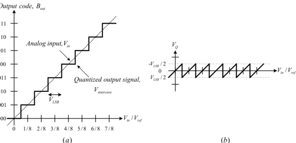
Figure 2.3 (a) shows the transfer curve for an ideal 3-bit ADC and the corresponding quantization noise is shown in Figure 2.3 (b) [6]. Note that the quantization noise is
limited to ±VLSB/ 2. / in ref V V , out Output code B Q V -VLSB/ 2 / 2 LSB V LSB V in Analog input, V staircase
Quantized output signal, V 000 001 010 011 100 101 110 111 0 1/ 8 2 / 8 3/ 8 4 / 8 5 / 8 6 / 8 7 / 8 / in ref V V 0 ( )a ( )b
In a stochastic approach, we assume that the input signal is varying rapidly such that
the quantization noise signal, V , is a random variable uniformly distributed between Q
/ 2
LSB
V
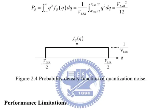
± . The probability density function for such an noise signal, f q , will be a Q
( )
constant value, as shown in Figure 2.4. Hence, the quantization noise power, P , is Q
given by
( )
/ 2 2 2 2 - - / 2 1 12 LSB LSB V LSB Q Q V LSB V P q f q dq q dq V ¥ ¥ =ò
=ò
= (2.5) -2 LSB V 2 LSB V q ( ) Q f q LSB 1 VFigure 2.4 Probability density function of quantization noise.
2.2.3 Performance Limitations
Before proceeding, it is required to know the performance metrics for determining the transfer response of the data converters. In this section, some commonly used terms characterizing the performance of data converters are introduced as below.
2.2.3.1 Resolution
The resolution of an ADC is defined to be the number of the distinct input segments corresponding to the different output word. It also indicates the minimal difference of the input signal that can be recognized by the ADC. An N-bit resolution
ADC means that the converter can resolve 2N distinct input segments. We can find
resolution ADCs. This quantity does not mean actually the accuracy of the converter, but instead it usually refers to the number of output bits.
2.2.3.2 Signal-to-Noise Ratio (SNR)
The signal-to-noise ratio (SNR) is the ratio of the signal power to the output noise power. The SNR includes the quantization noise and other circuits noise excluding the harmonic components of the input signal. If it is assumed that the input signal is a
sinusoidal waveform between 0 and V , then the RMS value of the sinusoidal wave ref
is equal to Vref / 2 2
( )
. If we only consider the quantization noise of the ADCs, themaximum SNR of an N-bit ADC is
( ) ( )
( )
( )
10 10 10 / 2 2 320log 20log 20log 2
2 / 12 6.02 1.76 ref in rms N Q rms LSB V V SNR V V SNR N dB æ ö æ ö æ ö ç ÷ ç ÷ = ç ÷= ç ÷= çç ÷÷ è ø è ø è ø = + (2.6)
However, the SNR decreases from the best possible value for reduced the input signal levels [4].
2.2.3.3 Signal-to-Noise plus Distortion Ratio (SNDR)
The signal-to-noise plus distortion ratio (SNDR) is often used to measure the performance of an ADC. When a sinusoidal signal is applied to an ADC, the output spectrum generally contains a single tone at the fundamental frequency. Due to distortion, the output spectrum also contains several tones at the harmonic frequency, known as harmonic distortion. As a result, the SNDR of the ADC is defined as the ratio of the signal power at the fundamental frequency to the total power of non-ideal effects, including the harmonic distortion, quantization noise and other noise sources
2.2.3.4 Spurious Free Dynamic Range (SFDR)
The spurious free dynamic range is defined as the power ratio of the input signal to the largest distortion component. In a fully differential signal system, generally the
largest distortion component is the 3rd harmonic term.
For more clearly figuring out the difference among SNR, SNDR and SFDR, a spectrum diagram is shown in Figure 2.5, where S is the fundamental frequency of the input signal, D are the distortion components and N is the noise floor.
Power Spectrum f S N D SFDR in f 2fin 3fin
Figure 2.5 The spectrum diagram with signal, distortion and noise.
The SFDR is depicted in Figure 2.5, and the SNR and SNDR are depicted as below respectively. S S SNR SNDR N N D = = + (2.7)
2.2.3.5 Effective Number of Bits (ENOB)
Another specification often used to describe the ADC’s performance is the effective number of bits (ENOB). Different from resolution, ENOB indicates the ADC’s accuracy in a specific input frequency and sampling rate, and it can be expressed from SNDR as follow:
-1.76 6.02 SNDR
ENOB= bits (2.8)
2.2.3.6 Offset and Gain Error
The transfer characteristic of an ADC is expected to be a straight line with uniform step width. However, the actual transfer step widths might not be uniform ideally. These non-ideal terms cause errors and non-linearity performance in ADCs. Figure 2.6 (a) shows the offset error, which is defined as the horizontal deviation from the ideal position by a constant amount. The gain error (or scale factor error) describes the difference of slop between the ideal straight line and the actual transfer line, as shown in Figure 2.6 (b). Input Output actual ideal ( )a ( )b Offset Error Gain Error actual ideal Output Input
Figure 2.6 Illustrating (a) offset error and (b) gain error for a 3-bit A/D converter.
2.2.3.7 Differential Non-Linearity Error (DNL)
After both the offset and gain errors have been removed, each transfer step level might not be equal to 1 LSB (
2
ref N
V
( )
, 1 1 step n Width LSB DNL n LSB -= (2.9)An ADC is guaranteed not to have any missing codes if the minimum DNL error is larger than -1 LSB.
2.2.3.8 Integral Non-Linearity Error (INL)
The integral non-linearity error is defined as the deviation of the middle point of each transfer step form the ideal straight line. There are two ways to define the straight line. A common used definition is known as the endpoint straight line which is drawn through the end points of the first and last code transition. An alternative definition is to find the best-fit straight line such that the maximum INL is minimized [4]. The INL is also specified after both the offset and gain errors have been removed and can be expressed as
( )
( ), ( ), 1 t n actual t n ideal V V INL n LSB -= (2.10)Figure 2.7 shows the illustration of the DNL and INL.
Input Output
actual
ideal
INL
1 LSB1
DNL
+
LSB
2.2.3.9 Sampling-Time Uncertainty (Aperture Jitter)
The sampling-time uncertainty is another significant issue that limits the performance of ADCs, which is also known as aperture jitter. Considering a
sinusoidal wave input signal, V , with input frequency in f as below in
( )
sin 2(
)
2 ref in in V V t = p f t (2.11)Since the variance of V for a sinusoidal waveform is the largest at the zero crossing in
point, we can find out the maximum slope by differentiating V with respect to time in
and setting t=0, as shown below
max in in ref V f V t p D = D (2.12)
If Dt represents the sampling-time uncertainty, and if we want to keep DVin less
than 1 LSB, we can find that
in in ref LSB
V p f V t V
D = D < (2.13)
In consequentially, we get the limit of the aperture jitter Dt of a N-bit ADC as
follows 1 2 LSB N in ref in V t f V f p p D < = (2.14)
2 ref V 2 ref V -0 in
V
t
t
D
inV
D
Sampling TimeFigure 2.8 Aperture jitter.
2.2.3.10 Dynamic Range (DR)
The dynamic range is defined as the ratio between the maximum signal power for peak SNR and the minimum detectable signal power within a specified bandwidth. With a sinusoidal input signal, we can measure the dynamic range by varying its amplitude to find the 0dB SNR and peak SNR positions, as shown in Figure 2.9. If the noise power is independent on the signal power, the dynamic range is equal to the SNR at full scale. However, generally the noise power increases as the signal power increases. Therefore, the actual peak SNR will be less than the dynamic range [3].
Dynamic Range ( ) SNR dB ( ) Vin dB Peak SNR 0 dB
2.3 Review of Nyquist-Rate A/D Converter Architecture
Architectures for implementing analog-to-digital converters (ADCs) can be roughly divided into three categories (Table 2.1)—low-to-medium speed, medium speed, and high speed. These different architectures of ADCs are developed for different applications. Each of them has different trade-off among speed, resolution, power, and area. In the section, Nyquist-rate A/D converters are introduced. These ADCs generate a series of output codes in which each code has a one-to-one correspondence with a single input value. With high operation speed near the Nyquist rate, these ADCs are good for high speed application. Another kind of ADCs is known as oversampling A/D converters, which are not introduced in this section. These ADCs operate much faster than the input signal’s Nyquist rate and increase the signal-to-noise ratio (SNR) by filtering out quantization noise. Generally, the oversampling ADCs are adopted for high resolution design.
Table 2.1 Different A/D converter architectures [4].
Low-to-Medium Speed, High Accuracy Medium Speed, Medium Accuracy High Speed, Low-to-Medium Accuracy Integrating Oversampling Successive approximation Algorithmic Flash Two-step Interpolating Folding Pipelined Time-interleaved
2.3.1 Flash (or Parallel) ADC
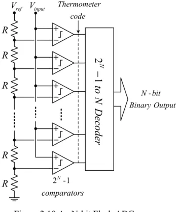
Flash ADCs, also known as Parallel ADCs, have the highest speed in overall ADC architectures. As seed in Figure 2.10, a flash ADC is composed with a resistor
string、2N-1 comparators and a (2N-1)-to-N decoder. The resistor string contains 2N
resistors and divides the reference voltage into 2N-1 segment values, and each of
which is fed to a comparator’s negative input. The input voltage is compared with each segment value and results in a thermometer code at the output of the comparators.
The thermometer exhibits all ones at the bottom if Vinput is great then the voltage on
the resistor string, and zeros at the top if Vinput is less then the voltage on the resistor
string. Finally, an (2N-1)-to-N decoder is used to convert the (2N-1)-bit thermometer
code into an N-bit binary output code. It is obvious that all comparators operate in parallel, and then the decoder deals with the output codes of these comparators immediately. Therefore, flash ADCs can generate a digital output word in each clock phase. Besides, the conversion speed of the flash ADC is only dependent on the speed of the comparators and the digital decoder, so it is easy to achieve high speed. With extremely high throughput, the flash ADC is quite suitable for very high speed application. However, for high resolution flash ADCs, a larger number of comparators and small offset for these comparators are required. Design of a comparator with small offsets is difficult and expensive. Furthermore, a large number of comparators induces a large input capacitive loading limiting the conversion rate and consumes large power and area. For above reasons, high resolution ADCs are rarely implemented by flash architectures.
ref V Vinput R R R R R N
to
N
D
ec
od
er
-N bit Binary Output 2 -1N comparators Thermometer codeFigure 2.10 An N-bit Flash ADC.
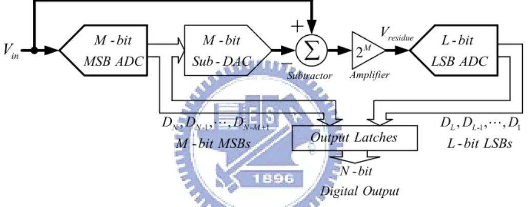
2.3.2 Two-Step ADC
Accompanying the increase of resolution, the flash ADC becomes nearly impossible to be realized for too large power consumption and area. One way to solve this problem is to separate the converter into two complete flash ADCs, which is known as two-step ADC. A two-step ADC mainly consists of a MSB ADC and a LSB ADC, which are used to convert the former bits and the later bits separately. As shown in Figure 2.11, we assume the MSB ADC is an M-bit converter and the LSB ADC is an L-bit converter, so the Sub-DAC must be an M-bit converter and the total output resolution, N, is equal to the sum of M and L. First, the input signal is quantized by the MSB ADC, and then the Sub-DAC would convert the first M-bit output code back to analog signal. This analog signal would be subtracted from the
input signal, and then the result would be multiplied by 2M. The output value of the
LSB ADC to determine the last L-bit output code, and then the total N-bit output code is accomplished by combining the first M-bit output and the last L-bit output. By applying the two-step architecture, the number of required comparators can be
reduced greatly from original 2N-1 to 2M+2L-2 (if M=L=N/2, it is equal to 2*(2(N/2)-1))
only. Therefore, it would be possible to realize high resolution ADC by using two-step architecture. However, the two-step ADC requires two clock cycle to generate one digital output word, so the speed of two-step ADC is slower than the flash ADC, which only needs one clock cycle [7].
M bit -MSB ADC -M bit Sub DAC
å
+
2M -L bit LSB ADC Subtractor Amplifier in V -1 - 1 , , , -N N N M D D D M bit MSBs + L , -1, , 1 -L L D D D L bit LSBs L Output Latches -N bit Digital Output residue VFigure 2.11 An N-bit Two-Step ADC.
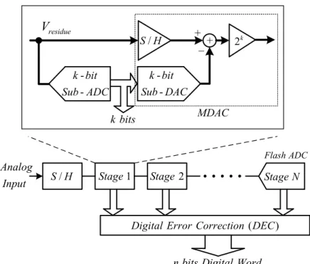
2.3.3 Pipelined ADC
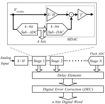
In two-step ADC, the ADC is divided into two steps, and it could be possible to separate the ADC into N steps, which is known as a pipelined ADC. As shown in Figure 2.12, a pipelined ADC consists of a S/H, several identical stages and a flash ADC in the final part. Each identical stage includes a Sub-ADC and a multiplying digital-to-analog converter (MDAC), which is composed of the S/H, the Sub-DAC, the subtractor and the gain amplifier.
/
S H Stage 1 Stage 2 Stage N
/ S H -k bit Sub ADC -k bit Sub DAC + _ + 2k residue V MDAC k bits
n bits Digital Word
( )
Digital Error Correction DEC Analog
Input
Flash ADC
Figure 2.12 An N-bit Pipelined ADC.
First, the input signal is sampled by the S/H and then the held value is fed to stage 1. The following identical stages sample the residue of the previous stage and process the signal likely a two-step ADC. The S/H in each stage allows stages to operate concurrently, so that each stage is free to process a new sample as soon as its residue is sampled by the next stage. Finally, the residue is fed to a flash ADC to determine the last bits. After an initial latency of N clock cycles, one conversion will be completed per clock cycle. Therefore, the pipelined ADC could still keep high throughput rate even though the number of stages increases. Because of the feature, pipelined ADCs can generally operate at much higher sampling rates.
With the inter-stage gain amplifiers, the requirement of the comparators for the following stages could be relaxed. Therefore, we could realize a high resolution pipelined ADC by only increasing the number of stages without raising the complexity of the comparators too much. However, the additional gain amplifiers would become the dominate sources of power dissipation. Therefore, pipelined ADCs
resolution applications, pipelined ADCs need fewer circuits compared to Flash and Two-Step ADCs, since the circuit complexity for pipelined ADCs approximately increase linearity but that is exponential growth in Flash and Two-Step ADCs. Because of the ability of each stage to operate concurrently and the tolerance of the comparator offsets, pipelined ADCs are quite suitable for high speed and medium-to-high resolution application [8].
2.3.4 Cyclic ADC
A cyclic ADC is similar to a single stage of pipelined ADCs with the output fed back to the input, as shown in Figure 2.13. It has only one stage and this stage would be repeatedly used in one cycle. When an input is sampled by the cyclic ADC, it takes N cycles to complete the output word and the delay time is the same as the pipelined ADC. However, the new input would not be sampled for a cyclic ADC before the N-bit output word is completed, so the throughput rate of the cyclic ADC is only 1/N times compared with the pipelined ADC. However, since only one stage is required, the cyclic ADC is extremely suitable for low power and low area designs.
/ S H -k bit Sub ADC -k bit Sub DAC + _ + 2k residue V k bits Input
2.3.5 Successive Approximation ADC
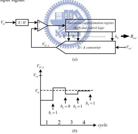
Successive-approximation ADCs apply a binary search algorithm to determine the closest digital word to match the input signal. As shown in Figure 2.14, it is also known as successive-approximation register (SAR) ADC. In the first cycle, the MSB,
b1, is determined and stored in the successive-approximation register (SAR), and then
b1 is fed to the D/A converter to generate a new reference value, VD/A. In the second
cycle, the original input signal is compared with the new VD/A to determine b2 and
then the same operation is repeated again. After N period cycles, the complete N-bit output word is determined. Successive approximation ADCs are very analogous to Cyclic ADCs, but in each cycle the former varies the reference voltage and the later varies the input signal.
Successive - approximation register (SAR) and control logic
/ D A converter / S H 1 b b2 bN / D A V in V ref V out B / D A V ref V cycle 1 1 b = 2 0 b = b3=1 1 2 3 4 in V 4 1 b = ( )a ( )b
Figure 2.14 (a) Successive-approximation converter and (b) transfer curve of VD/A.
2.3.6 Time-Interleaved ADC
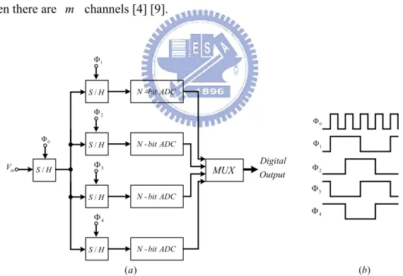
The time-interleaved ADC is realized by operating many identical ADCs in
parallel. Figure 2.15 shows a four-channel time-interleaved ADC. Here, F is a 0
clock at four times the rate of F to 1 F . The additional 4 F to 1 F are delayed 4
with respect to each other by the period of F , such that each converter will get 0
successive samples of the input signal, V , sampled at the rate of in F . In this way, 0
the throughput rate of the time-interleaved ADC is four times the rate of each ADC in the four channels. By using many ADCs in parallel, time-interleaved ADCs achieve high conversion rate but consume large power and area. It is also essential that the
channels are extremely well matched, as mismatches will introduce tones at fs /m
when there are m channels [4] [9].
( )a / S H 0 F in V / S H 1 F / S H 2 F / S H 3 F / S H 4 F N - bit ADC N - bit ADC N - bit ADC N - bit ADC
MUX OutputDigital
0 F 1 F 2 F 3 F 4 F ( )b
Chapter 3
Pipelined ADC with
Opamp-Sharing Technique and
Improved Loading-Free Architecture
3.1 Introduction
In this chapter, the proposed pipelined ADCs with opamp-sharing technique and improved loading-free architecture would be discussed in detail. Before these discussions, the basic blocks of pipelined ADCs and the calibration techniques are introduced first. With the calibration techniques, the nonlinearities occurring in pipelined ADCs could be compensated and the requirements of comparator offsets are also relaxed. Then, the most popular 1.5-bit/stage structure in pipelined ADC is presented. In this architecture, the inter stages have large bandwidth and can be realized by simple components. Thus, it is very suitable for high speed and low power design. For higher power- and area- efficiency, opamp-sharing technique is introduced first. This technique could significantly reduce the number of required opamps. Following, the loading-free architecture based on switched-opamp (SO) circuits is presented. SO structure is suitable for low voltage design since no floating switched is needed. By reducing the output capacitive loading, loading-free architecture can achieve higher operation speed than conventional SO circuits. For even more improving the loading-free architecture, the proposed new loading-free MDAC is developed, which has less output capacitive loading and larger feedback factor. A summary is placed in the last to describe the architectures of these two
3.2 Conventional 1.5-Bit/Stage Pipelined ADC
The detail components of pipelined ADCs are discussed following. Then, the calibration techniques are introduced, which overcome the nonlinearities and relax the requirement of comparators. After that, the most popular architecture, 1.5-bit/stage pipelined ADC, is introduced. It owns large tolerance to the offset of comparators and is easy to be realized with simple components. Besides, the 1.5-bit/stage architecture is good for high speed design. In the final part, we discuss the requirements of gain and speed for pipelined ADCs.
3.2.1 Basic Blocks of Pipelined ADC
The block diagram of a typical pipelined ADC is shown in Figure 3.1, including a S/H, several identical stages, a flash ADC, delay elements and a digital error correction (DEC) logic. The S/H relaxes the timing requirement of the first stage, since the first stage can sample a static signal from the S/H rather than a variant signal from the analog input. Following the S/H, several identical stages are in series. Within each stage, the analog input signal from the previous stage is sampled and fed to the Sub-ADC to resolve k bits. Then, the quantized value from the Sub-DAC is subtracted from the original analog input to yield the output residue. Finally, the residue is
multiplied by the amplifier with a gain of 2k in order to maintain the input signal
range equal to the output signal range for each stage. The S/H, Sub-DAC, subtraction and the amplification are combined into one single circuit called multiplying digital-to-analog converter (MDAC). The last signal is fed into a Flash ADC to determine the last bits. Since the former bits are generated early, the delay elements are required for synchronizing the output codes. By passing the digital error correction (DEC) logic, the final output digital word is completed [3] [4].
/
S H Stage 1 Stage 2 Stage N
/ S H -k bit Sub ADC -k bit Sub DAC + _+ 2k residue V MDAC k bits
n bits Digital Word
( )
Digital Error Correction DEC Analog
Input
Flash ADC
Delay Elements
Figure 3.1 The block diagram of a k-bit/stage pipelined ADC.
The timing diagram for a pipelined ADC is shown in Figure 3.2. The pipelined ADC needs two clock phases for each conversion. One clock phase is used for sampling the input signal, and the other is employed for processing and holding the residue voltage. Since the hold residue voltage in current stage has to be sampled by the next stage, the consecutive stages must operate in opposite clock phase. Thus, the latency in clock cycle is a half of the number of stages. Besides, since each stage is free for processing a new sample as soon as its residue is sampled by the next stage, the pipelined ADC is good for operating concurrently and gives a throughput of one output sample per clock cycle [10] [11].
sample hold A/D
sample hold sample hold
sample hold sample hold sample hold sample
A/D A/D sample hold A/D sample sample hold A/D A/D S/H Stage 1 Stage 2 MDAC Sun-ADC MDAC Sun-ADC t
An example of 2-bit per stage is shown in Figure 3.3(a). The 2-bit ADC divides the full scale input range into four subranges, and each subrange is corresponding to a given 2-bit digital code. According to the digital code, the input signal subtracts the output of the DAC to get the residue value. For restored the original full scale input range, the residue value is multiplied by the amplifier with the gain of 4, so the output value for each stage is
(
)
4
out in DAC
V = V -V (3.1)
As shown in Figure 3.3(b)(c), the residue plot is in the shape of sawtooth with the full
scale range between Vref and –Vref [12].
/ S H 2 - bit ADC 2 - bit DAC + _+ 4 out V 2 bits in V DAC V 00 01 10 11 ref V - 1 2Vref - 1 2Vref 0 Vref ref V ref V -3 4Vref 1 4Vref 3 4Vref -1 4Vref -DAC V in V in V out V ref V ref V -ref V - 1 2Vref - 1 2Vref 0 Vref 11 10 01 00 0 ( )a ( )b ( )c
Figure 3.3 (a) Block diagram for 2-bit/stage
3.2.2 Nonlinearities and Calibration Techniques
For a general pipelined ADC, the output signal range is equal to the input signal range of each stage. If the output signal range is larger than the input signal range of the next stage, the following stages would solve the wrong codes and the missing codes may also appear. The output signal range is determined by the gain of the residue amplifier which is used to amplify the residue voltage. For an ideal 2-bit per stage pipelined ADC, the gain of the residue amplifier is four. So that, the gain error of the residue amplifier will induce the over range problem, as shown in Figure 3.4(a). Another non-ideal issue also causing the over range problem is the comparator offset of the Sub-ADC, as shown in Figure 3.4(b). The comparator offset would shift the transition level and make the transfer curve exceed the signal range.
in V out V ref V ref V -ref V - 1 2Vref - 1 2Vref 0 Vref 11 10 01 00 0 in V out V ref V - 1 2Vref - 1 2Vref 0 Vref 11 10 01 00 ( )a in V out V ref V ref V -ref V - 1 2Vref - 1 2Vref 0 Vref 11 10 01 00 0 in V out V ref V - 1 2Vref - 1 2Vref 0 Vref 11 10 01 00 ( )b ideal actual ideal actual ideal actual ideal actual
In order to prevent the over range problem, the inter stage gain is half reduced so that the amplified residue can remain within the conversion range of the next stage no matter what kind of error exists. To illustrate the calibration technique in more detail, we take a 2-bit per stage pipelined ADC for example. When the inter stage gain is
reduced to 2, the residue range is compressed between 1/2 Vref and -1/2 Vref,
illustrated in Fig 3.5 (a). If the comparator offset is less than ±1/4Vref, the residue
would still be within Vref and –Vref. The following stage could correct the output codes
by adding or subtracting correction, as shown in Figure 3.5 (b). When one of the transition level of the sub-ADC has an offset, the output of this stage will exceeds
±1/2 Vref. The next stage, sensing the overhanging, will add or subtract the output by 1
LSB, and this is known as digital error correction (DEC) technique. It allows the
comparator offset to be as large as ±1/4 Vref and the output is still in the input range
of the following stage. Digital error correction simply utilizes the extra bit to correct the overhanging section from the previous stage.
in V out V ref V ref V -ref V - 1 2Vref - 1 2Vref 0 Vref 11 10 01 00 0 ideal actual in V out V ref V - 1 2Vref - 1 2Vref 0 Vref 11 10 01 00 ideal actual 1 2Vref 1 2Vref -ref V 0 1 2Vref 1 2Vref -Addition correction Subtraction correction ( )a ( )b
Figure 3.5 (a) the residue plot of 2-bit/stage with inter stage gain of 2 (b) with comparator offset.
Since subtraction is equivalent to addition with offset, we could eliminate subtraction by intentionally adding a 1/2 LSB offset to both sub-ADC and DAC, as shown in Figure 3.6. After shifting 1/2 LSB offset in the transition level, the subranges are separated in different width. The section of “00” is enlarged and that of “11” is reduced. Because the inter stage gain is 2, the amplified residue remains within the conversion range of the next stage when the offset of comparators are
between ±1/4Vref. Under these conditions, errors caused by the sub-ADC nonlinearity
can be corrected, and the correction requires no change and addition.
/ S H 2 - bit ADC 2 - bit DAC + _+ 2 out V 2 bits in V in V out V ref V ref V -ref V - 1 4Vref - 3 4Vref 1 4Vref Vref 11 10 01 00 0 ( )a ( )b 1 2 LSB Offset _ + + + + + ideal 1 2 shift LSB
Figure 3.6 (a) Block diagram of one stage with 1/2 LSB offset in ADC and DAC (b) residue plot versus held input with 1/2 LSB offset.
Since the last transition level is only 1/2 LSB below the maximum stage input, we can assume that the decision level of the top comparator has an offset of 1/2 LSB adding and it is shifted to the upper bound of the conversion range, as shown in Figure 3.7(b). The digital output code “11” is eliminated. However, the output code “11” can be recovered by the digital error correction of the next stage and the output residue is still within the conversion range. According to this assumption, removal of the top-most comparator does not change the correction range, since the transition level
can still move by up to ±1/2 LSB before saturating the next stage [12] [13]. This
architecture only needs two comparators at 1/4 Vref and -1/4Vref for each Sub-ADC
and three reference voltages at at -1/2Vref, 0, 1/2Vref for each Sub-DAC. Since only
three codes (00, 01 ,10) are solved per stage, it is known as 1.5-bit/stage pipelined ADC architecture. The digital error correction logic corrects the wrong code by adding the first bit of the next stage to the previous stage, so only 1 bit full adders are used in the correction logic, as shown in Figure 3.8.
/ S H 1.5 -bit ADC 1.5 -bit DAC + _+ 2 out V 2 bits in V in V out V ref V ref V -ref V - 1 4Vref - 1 4Vref Vref 10 01 00 0 ( )a ( )b ideal 1.5 bit
Figure 3.7 (a) Block diagram of 1.5-bit per stage
(b) residue plot versus held input without top comparator.
N
B0
N
B1
Full Adder Full Adder
N
D DN-1
N-1
B1 B0N-1
3.2.3 1.5-Bit/Stage Architecture
The number of bits per stage determines the speed, accuracy and power requirements for each stage. Therefore, the best choice of the bit number is dependent on the specification for the overall ADC. With fewer numbers of bits per stage, fewer comparators are required for each Sub-ADC and the comparator requirements are more relaxed. Besides, accuracy requirement is also reduced which allows the stage operating in higher speed due to the fundamental gain bandwidth tradeoff of amplifiers. However, for fewer numbers of bits, more stages are required and the lower accuracy also contributes much noise to the overall conversion. Therefore, lower number of bits is much suitable for high speed, low resolution design.
The 1.5-bit per stage architecture has been shown to be effective in achieving high sampling rate with medium-to-high resolution [12] [14]. An 8-bit pipelined ADC using 1.5-bit per stage architecture is shown in Figure 3.9. The 1.5-bit per stage architecture is employed in the first 6 stage, and the last stage is composed of a 2-bit Flash ADC. By combining the 12 bits from the first six stages and last 2 bits from the Flash ADC, the digital error correction logic produces the final 8-bit output code.
Each stage resolves 2 bits output code with the Sub-ADC, subtracts the output value of the Sub-DAC from its input and amplifies the residue by a gain of 2. The Sub-ADC is characteristic of only 3 digital output codes (00, 01, and 10) and has
thresholds at Vref/4 and –Vref/4. The residue plot has been shown in Figure 3.7 (b) and
the residue transfer function can be expressed as
2 2 2 2 , 1 4 (10) 2 , 1 4 1 4 (01) 2 , 1 4 (00) in ref ref in
out in ref in ref
in ref in ref V V if V V D V V if V V V D V V if V V D ì - < = ï =í - < < = ï + < - = î (3.2)
/
S H Stage 1 Stage 2 Stage 7
/ S H 1.5 -bit Sub ADC 1.5 -bit Sub DAC + _ + x2 in V MDAC 2 bits
8 bits Digital Word
( )
Digital Error Correction DEC Analog Input Flash ADC Delay Elements 6 Stage 2 - bit out V
2 bits 2 bits 2 bits 2 bits
14 bits
Figure 3.9 Block diagram of 1.5-bit-stage pipelined ADC.
Figure 3.10 illustrates one method to implement the 1.5-bit per stage architecture by using the switched-capacitor circuit. This circuit operates on a two-phase clock. In
the first phase, the input signal, Vin, is applied to the Sub-ADC, which has two
thresholds at ±Vref/4, to solve the 2-bit output code. At the same time, Vin is also
sampled in the capacitors Cs and Cf. In the next phase, Cf closes a negative feedback
loop around the opamp, while the top plate of Cs is switched to the DAC output.
4 ref V -+ 4 ref V -+ + L A T CH ref V 0 -Vref MUX + -1 S 2 S 3 S f C s C in V out V
-SUB ADC DAC 2 X GAIN
According the 2-bit output code, the reference voltages (Vref, 0, -Vref) would be
determined by the DAC and the output voltage can be expressed as
s s f f s f s s f f C C 1+ , 1 4 C C C 1+ , 1 4 1 4 C C C 1+ , 1 4 C C in ref ref in
out in ref in ref
in ref in ref V V if V V V V if V V V V V if V V ìæ ö - < ïç ÷ è ø ï ïæ ö ï =íç ÷ - < < è ø ï ïæ ö ïç ÷ + < -ïè ø î (3.3)
For 1.5-bit per stage architecture, Cs = Cf is chosen to get a stage gain of two. Since
only two comparators are required and the requirements of the comparators are very relax, the amplifier becomes the best part of power consumption.
3.2.4 Accuracy Requirements
The accuracy requirement on each stage of a pipelined ADC is different because the resolution for each stage output is decreased by the number of bit solved per stage. For example, in an N-bit pipelined ADC with B-bit effective resolution per stage, the first stage has to meet N bits resolution requirement and the next stage only need to meet N-B bits resolution requirement. The lower resolution requirement relax the requirements of the inter stage gain amplifier, capacitor mismatch and the thermal noise effect. f C =C (2B 1) s C = - C 1 f C + 1 s C +
+
_
+
_
DAC V , out i VStage i
Stage i
1
+
Figure 3.11 illustrates a switched-capacitor MDAC circuit. Assuming that this is an N-bit resolution pipelined ADC and the stage i is the first stage. Since each stage solves B bits effective resolution, the output of the first stage has only to meet N-B bits resolution requirement. Considering the nonidealities of the inter stage amplifier that introduce the finite opamp gain, the output value can be expressed as
(
)
out i in DAC V =G V× -V (3.4) 1 1 1 1 t s f i f C C G e C Af t -æ ö ç ÷ æ + ö æ ö ç ÷ =çç ÷÷ç ç - ÷ ÷è ø è ø +ç ÷ è ø (3.5) f s f op amp C f C C C -= + + (3.6)where f is the feedback factor as expressed in Equation (3.6). The exponential term represent the finite settling time t of the single pole opamp, where the τ is the time constant for the SC configuration, and the A is the finite opamp gain. For a infinite
opamp DC gain, the ideal inter stage gain Gi can be known as
(
2 1)
2 B s f B i f C C C C G C C - + + = = = (3.7)In order to meet the N-B bits resolution requirement for the next stage, the finite gain error of the inter stage should be theoretically less than 1/2 LSB and it can be described as 1 actual ideal rr ideal G G G Af e = - = (3.8)
Therefore, we can get
1 1 1
2 2
rr Af N B
Combining Equations (3.6) and (3.9), the limit of finite gain for the inter stage amplifier can be expressed as following
1 1 2 1 1 2 2 2 B s f op amp op amp N B N B N B f C C C C C A f C C - -- + + + - + + - + > ´ = ´ = ´ (3.10)
If Cop-amp is small enough to be neglected, Equation 3.10 is equal to 2N+1 and this is
the minimum requirement of A for the first stage. Increasing the number of bit per stage solved does not enhance the minimal required gain of the amplifier. In practice, the opamp gain should be much larger than this value since errors caused by other sources such as incomplete settling and capacitor-mismatch are not taken into account.
After considering the gain requirement of the inter stage amplifier, the finite settling time of the switch-capacitor circuit is discussed. The speed constraints influencing the accuracy include the slew time for large signal and the settling time for small signal. The slew time is related to the tail current and the output load capacitance of the inter stage opamp; while the settling time depends on the unity-gain
frequency (fu) and the phase margin of the opamp, and the feedback factor (f) of the
close-loop circuit.
Referring to Equation (3.5), the settling error can be expressed as following
,
t rr settle e
t
e = - (3.11)
where τ is the time constant of the close-loop circuit. For a single pole opamp switched-capacitor circuit, the time constant is equal to
3 1 1 2 dB fu f t w p = = × × (3.12)
where ω3dB is the close-loop bandwidth, fu is the unity-gain frequency of the amplifier
For the same reason to meet the N-B bits resolution requirement, the settling error of output response must less than 1/2 LSB.
, 1 1 2 2 settle T rr settle e N B t e -= < × (3.13)
According to Equation (3.12) and (3.13), we can obtain the required minimum
unity-gain frequency fu of the amplifier as following
(
1 ln 2)
(
1 ln 2)
2 2 2 op amp B u settle settle C N B N B f T f T C p p -- + × - + × æ ö > = ×ç + ÷ × × × è ø (3.14)where Tsettle is the allowed settling time and it is usually 75%~90% of half conversion
period. From above equation, higher unity-gain frequency is required to sustain the accuracy for larger number of bit per stage solved, B.
Another nonideality that also influences the accuracy is the capacitor-mismatch effect due to the process variation. The required matching of the sampling and feedback capacitors in MDAC are determined by the required DAC accuracy.
Assuming that the value of the capacitors deviates by ΔC, which makes Cs = C+ΔC/2
and Cf = C-ΔC/2, the output of the MDAC is given by
2 1 out in DAC C C V V V C C D D æ ö æ ö =ç + ÷ ± +ç ÷ è ø è ø (3.15)
From Equation (3.15), the error term ΔC/C must be less than 1/2N-B to ensure that
offset of DAC is less than 1 LSB.
1 2N B C C -D < (3.16) In addition to above deterministic errors, the thermal noise KT/C also causes random errors in the SC circuits. As we known larger capacitors tend to have better matching property and less thermal noise contribution than smaller capacitors. However, smaller capacitors provide less loading and faster settling for enabling high speed. In the other word, the thermal noise can be reduced by increasing the size of
![Figure 2.8 shows the concept of the aperture jitter [4].](https://thumb-ap.123doks.com/thumbv2/9libinfo/8462437.183232/26.892.147.759.495.718/figure-shows-concept-aperture-jitter.webp)
![Table 2.1 Different A/D converter architectures [4].](https://thumb-ap.123doks.com/thumbv2/9libinfo/8462437.183232/28.892.160.730.769.993/table-different-a-d-converter-architectures.webp)